EP4293866A1 - Appareil et procédés pour fournir une alimentation de charge à un dispositif externe - Google Patents
Appareil et procédés pour fournir une alimentation de charge à un dispositif externe Download PDFInfo
- Publication number
- EP4293866A1 EP4293866A1 EP23179908.1A EP23179908A EP4293866A1 EP 4293866 A1 EP4293866 A1 EP 4293866A1 EP 23179908 A EP23179908 A EP 23179908A EP 4293866 A1 EP4293866 A1 EP 4293866A1
- Authority
- EP
- European Patent Office
- Prior art keywords
- power
- conductive plate
- coupled
- current
- terminal
- Prior art date
- Legal status (The legal status is an assumption and is not a legal conclusion. Google has not performed a legal analysis and makes no representation as to the accuracy of the status listed.)
- Pending
Links
Images



Classifications
-
- H—ELECTRICITY
- H02—GENERATION; CONVERSION OR DISTRIBUTION OF ELECTRIC POWER
- H02J—ELECTRIC POWER NETWORKS; CIRCUIT ARRANGEMENTS OR SYSTEMS FOR SUPPLYING OR DISTRIBUTING ELECTRIC POWER; SYSTEMS FOR STORING ELECTRIC ENERGY
- H02J7/00—Circuit arrangements for charging or discharging batteries or for supplying loads from batteries
- H02J7/70—Circuit arrangements for charging or discharging batteries or for supplying loads from batteries characterised by the mechanical construction
-
- B—PERFORMING OPERATIONS; TRANSPORTING
- B60—VEHICLES IN GENERAL
- B60L—PROPULSION OF ELECTRICALLY-PROPELLED VEHICLES; SUPPLYING ELECTRIC POWER FOR AUXILIARY EQUIPMENT OF ELECTRICALLY-PROPELLED VEHICLES; ELECTRODYNAMIC BRAKE SYSTEMS FOR VEHICLES IN GENERAL; MAGNETIC SUSPENSION OR LEVITATION FOR VEHICLES; MONITORING OPERATING VARIABLES OF ELECTRICALLY-PROPELLED VEHICLES; ELECTRIC SAFETY DEVICES FOR ELECTRICALLY-PROPELLED VEHICLES
- B60L53/00—Methods of charging batteries, specially adapted for electric vehicles; Charging stations or on-board charging equipment therefor; Exchange of energy storage elements in electric vehicles
- B60L53/10—Methods of charging batteries, specially adapted for electric vehicles; Charging stations or on-board charging equipment therefor; Exchange of energy storage elements in electric vehicles characterised by the energy transfer between the charging station and the vehicle
- B60L53/14—Conductive energy transfer
- B60L53/16—Connectors, e.g. plugs or sockets, specially adapted for charging electric vehicles
-
- B—PERFORMING OPERATIONS; TRANSPORTING
- B60—VEHICLES IN GENERAL
- B60L—PROPULSION OF ELECTRICALLY-PROPELLED VEHICLES; SUPPLYING ELECTRIC POWER FOR AUXILIARY EQUIPMENT OF ELECTRICALLY-PROPELLED VEHICLES; ELECTRODYNAMIC BRAKE SYSTEMS FOR VEHICLES IN GENERAL; MAGNETIC SUSPENSION OR LEVITATION FOR VEHICLES; MONITORING OPERATING VARIABLES OF ELECTRICALLY-PROPELLED VEHICLES; ELECTRIC SAFETY DEVICES FOR ELECTRICALLY-PROPELLED VEHICLES
- B60L2200/00—Type of vehicles
- B60L2200/10—Air crafts
-
- B—PERFORMING OPERATIONS; TRANSPORTING
- B60—VEHICLES IN GENERAL
- B60L—PROPULSION OF ELECTRICALLY-PROPELLED VEHICLES; SUPPLYING ELECTRIC POWER FOR AUXILIARY EQUIPMENT OF ELECTRICALLY-PROPELLED VEHICLES; ELECTRODYNAMIC BRAKE SYSTEMS FOR VEHICLES IN GENERAL; MAGNETIC SUSPENSION OR LEVITATION FOR VEHICLES; MONITORING OPERATING VARIABLES OF ELECTRICALLY-PROPELLED VEHICLES; ELECTRIC SAFETY DEVICES FOR ELECTRICALLY-PROPELLED VEHICLES
- B60L2240/00—Control parameters of input or output; Target parameters
- B60L2240/40—Drive Train control parameters
- B60L2240/52—Drive Train control parameters related to converters
- B60L2240/529—Current
Definitions
- the present application relates to providing charging power to an external device, and more particularly, to apparatus and methods for providing charging power to an external device.
- a user When a device needs to be charged, a user usually needs to align the device's charging connector with a charger's connector before electrically connecting the device to the charger.
- the alignment may require additional attention and time from the user. It may cause inconvenience and inefficiency to the user.
- a device to be charged is an unmanned device, the unmanned device and/or a charger may require an additional mechanism for aligning their connectors. The additional mechanism may cause additional power consumption and/or cost increase and require additional operation time.
- Embodiments of the present application provide apparatus and methods for providing charging power to an external device.
- inventions include apparatus for providing charging power to a pair of external power charging terminals that are coupled to a power storage device of an external device.
- the pair of external power charging terminals are spaced apart by a predetermined distance.
- the apparatus includes a conductive plate assembly.
- the conductive plate assembly includes a plurality of conductive plates. Each of the conductive plates has a surface. The surface has a maximum surface length that is less than the predetermined distance. The maximum surface length is greater than or equal to a length between any two points on the surface of the conductive plate.
- the apparatus also includes a plurality of detector circuits respectively coupled to corresponding ones of the plurality of conductive plates.
- Each of the detector circuits is configured to be responsive to a voltage on one of the external power charging terminals to provide a detection signal when the corresponding conductive plate contacts the one of the external power charging terminals.
- the apparatus also includes a plurality of selection circuits respectively coupled to corresponding ones of the plurality of conductive plates and including a pair of power-supply terminals for receiving a power supply voltage.
- Each of the selection circuits is further coupled to receive the detection signal from a corresponding one of the detector circuits and configured to electrically connect the corresponding conductive plate to one of the power-supply terminals in response to receiving the detection signal.
- inventions also include apparatus for providing charging power to a pair of external power charging terminals that are coupled to a power storage device of an external device.
- the pair of external power charging terminals are spaced apart by a predetermined distance.
- the apparatus includes a conductive plate assembly.
- the conductive plate assembly includes a plurality of conductive plates.
- the apparatus also includes a plurality of detector circuits respectively coupled to corresponding ones of the plurality of conductive plates.
- the plurality of detector circuits is coupled to an electrically common circuit point.
- Each of the detector circuits is configured to be responsive to a voltage on one of the external power charging terminals to provide a detection signal when the corresponding conductive plate is contacted by the one of the external power charging terminals.
- the apparatus also includes a plurality of selection circuits respectively coupled to corresponding ones of the plurality of conductive plates.
- the selection circuits include a pair of power-supply terminals for receiving a power supply voltage.
- Each of the selection circuits is further coupled to receive the detection signal from a corresponding one of the detector circuits and configured to electrically connect the corresponding conductive plate to one of the power-supply terminals in response to receiving the detection signal.
- These embodiments further include a method for providing charging power to a pair of power charging terminals that are coupled to a power storage device.
- the method includes detecting that a first of a plurality of conductive plates is contacted by a first of the power charging terminals based on a first current.
- the method also includes detecting that a second of the plurality of conductive plates is contacted by a second of the power charging terminals based on a second current.
- the second current is sourced from the first current, or the first current is sourced from the second current.
- the method further includes electrically connecting the first conductive plate to a first of a pair of power-supply terminals.
- the method also includes electrically connecting the second conductive plate to a second of the pair of power-supply terminals.
- the method further includes providing charging power to the pair of power charging terminals from the pair of power-supply terminals via the first and second conductive plates.
- Disclosed embodiments include apparatus for providing charging power to a pair of external power charging terminals that are coupled to a power storage device of an external device.
- the external device includes a laptop, a tablet, a smartphone, an appliance, an electronic component, a gadget, a machine, a medical device, a vehicle, an unmanned vehicle, an automatic vehicle, or any other apparatus having a power storage device to be charged.
- the power storage device of the external device may be a rechargeable battery, a secondary battery, a storage battery, an electrostatic double-layer capacitor, an electrochemical pseudocapacitor, a hybrid capacitor, a lithium-ion capacitor, or any other energy storage device or component.
- the power storage device of the external device is coupled to a pair of power charging terminals that are a part the external device or are terminals of a connection line or of a peripheral for power charging.
- the pair of power charging terminals are external to the apparatus for providing charging power and may be referred to as a pair of external power charging terminals in this disclosure.
- the pair of external power charging terminals are spaced apart by a predetermined distance.
- the predetermined distance is a distance that prevents two external power charging terminals from coupling to a same conductive plate of the apparatus for providing charging power. Additionally or alternatively, the predetermined distance may be a distance that ensures two external power charging terminals are coupled to two different conductive plates of the apparatus for providing charging power.
- the apparatus for providing charging power includes a conductive plate assembly that includes a plurality of conductive plates.
- the conductive plate assembly is an assembly to be coupled to the pair of external power charging terminals for providing charging power.
- two or more of the plurality of conductive plates are coupled to the pair of external power charging terminals to provide charging power.
- a conductive plate is a conductive component and used as a contact terminal to be coupled to one of the pair of external power charging terminals.
- Each of the conductive plates has a surface.
- the surface is used to be coupled to one of the pair of external power charging terminals.
- a shape of the surface may be a circle, a triangle, a square, a hexagon, a rectangle, or any other polygon.
- the surface has a maximum surface length. The maximum surface length is greater than or equal to a length between any two points on the surface of the conductive plate. The maximum surface length of the shape is less than the predetermined distance, by which the pair of external power charging terminals are spaced apart from each other. Accordingly, the two external power charging terminals are prevented from coupling to the same conductive plate. As a result, the two external power charging terminals are coupled to two or more different conductive plates of the conductive plate assembly for receiving charging power.
- FIG. 1A illustrates an exemplary unmanned aerial vehicle (UAV) 1100 and an exemplary conductive plate assembly 1200 for providing charging power to exemplary UAV 1100, according to some embodiments of the present disclosure.
- conductive plate assembly 1200 includes a plurality of conductive plates, including conductive plates 1210, 1220, 1230, 1240, 1212, 1222, 1232, and 1242, for providing charging power to UAV 1100.
- UAV 1100 includes four landing legs 1110, 1120, 1130, and 1140. Landing legs 1110 and 1120 include positive and negative power charging terminals, respectively.
- the positive power charging terminal at landing leg 1110 is spaced apart from the negative power charging terminal at landing leg 1120 by a distance D CT .
- UAV 1100 is an external device to conductive plate assembly 1200.
- UAV 1110 includes a battery (not shown) to be charged.
- the positive and negative power charging terminals at the landing legs 1110 and 1120 are coupled (not shown) to the battery.
- UAV 1100 lands, or is put, on conductive plate assembly 1200 so that the positive and negative power charging terminals at the landing legs 1110 and 1120 are coupled to, for example, conductive plates 1210 and 1230 at points P1 and P2, respectively, for receiving charging power.
- conductive plate assembly 1200 includes the plurality of conductive plates arranged as an array and separated from each other ( FIG. 1D ).
- Each of the conductive plates has, for example, a square surface.
- the square surface has a diagonal length that is a maximum surface length L SQR-MAX ( FIG. 1B ).
- the maximum surface length (L SQR-MAX ) is greater than or equal to a length between any two points on the surface of the conductive plate.
- the maximum surface length (L SQR-MAX ) of the conductive plate is greater than a side length between two points on two adjacent vertices.
- the maximum surface length (L SQR-MAX ) of the conductive plate is equal to a diagonal length of the conductive plate.
- the maximum surface length (L SQR-MAX ) of the conductive plate is less than the distance (D CT ) by which the positive power charging terminal at landing leg 1110 is spaced apart from the negative power charging terminal at landing leg 1120. Accordingly, the positive and negative power charging terminals at landing legs 1110 and 1120 are prevented from coupling to a same one of the conductive plates of conductive plate assembly 1200. As a result, the positive and negative power charging terminals of UAV 1100 are coupled to two or more different conductive plates of conductive plate assembly 1200 for receiving charging power. For example, as shown in FIG. 1A , the positive and negative power charging terminals at landing legs 1110 and 1120 of UAV 1100 are coupled to conductive plates 1210 and 1230, respectively.
- FIG. 1B illustrates exemplary shapes of conductive plates for exemplary conductive plate assembly 1200 in FIG. 1A , according to some embodiments of the present disclosure.
- a conductive plate may have a square surface.
- the square surface of the conductive plate has the maximum surface length L SQR-MAX .
- the maximum surface length (L SQR-MAX ) of the conductive plate is less than the distance (D CT ) between the two external charging terminals, as described above with reference to FIG. 1A .
- conductive plate assembly 1200 may have a plurality of conductive plates with hexagonal surfaces. As shown in the middle of FIG. 1B , a hexagonal surface of a conductive plate has a diagonal length between two opposite vertices as a maximum surface length L HEX-MAX . The maximum surface length (L HEX-MAX ) of the conductive plate is less than the distance (D CT ) between the two external charging terminals, similar to the description above for the square shape with reference to FIG. 1A .
- conductive plate assembly 1200 may have a plurality of conductive plates with circular surfaces. As shown in the right of FIG. 1B , a circular surface of a conductive plate has a diameter length as a maximum surface length L CIR-MAX . The maximum surface length (L CIR-MAX ) of the conductive plate is less than the distance (D CT ) between the two external charging terminals, similar to the description above for the square shape with reference to FIG. 1A .
- FIG. 1C illustrates maximum surface lengths of the exemplary shapes of conductive plates in FIG. 1B , according to some embodiments of the present disclosure. As shown in FIG. 1C , all of the maximum surface lengths (L SQR-MAX , L HEX-MAX , and L CIR-MAX in FIG. 2 ) are less than the distance (D CT ) between the positive and negative power charging terminals at landing legs 1110 and 1120.
- D CT the distance between the positive and negative power charging terminals at landing legs 1110 and 1120.
- the two contact points P+ and P- are spaced apart from each other by the distance D CT that is greater than any of the maximum surface lengths (L SQR-MAX , L HEX-MAX , and L CIR-MAX in FIG. 2 ). That is, the two contact points P+ and P- cannot be on a same conductive plate. This prevents a short circuit being formed between the positive and negative power charging terminals at the landing legs 1110 and 1120 when UAV 1100 lands, or is put, on conductive plate assembly 1200 in any orientation.
- FIG. 1D illustrates dimensions of exemplary conductive plate assembly 1200 in FIG. 1A , according to some embodiments of the present disclosure.
- conductive plate assembly 1200 includes conductive plates 1251, 1252, 1253, 1254, 1261, 1262, 1263, 1264, 1271, 1272, 1273, 1274, 1281, 1282, 1283, and 1284, each having a square surface.
- Each of the square surfaces has a maximum surface length (L SQR-MAX ).
- L SQR-MAX maximum surface length
- the gap has a gap width W GAP and a diagonal gap width W GAP-Diag .
- the gaps may include insulation materials or empty spaces that prevent any two adjacent conductive plates from electrically coupling to each other.
- the positive and negative power charging terminals at the landing legs 1110 and 1120 may contact two or more conductive plates at, for example, contact points P L + and P L - ( FIG. 1D ), with each of contact points having a large contact area, respectively.
- the large contact areas of contact points P L + and P L - have a dimension that is greater than the diagonal gap width (W GAP-Diag ) of the gap.
- the distance D CT that is greater than the maximum surface length (L SQR-MAX ) can ensure the two external power charging terminals at the landing legs 1110 and 1120 contact two or more different conductive plates of conductive plate assembly 1200, as shown in FIG. 1D .
- the positive and negative power charging terminals at the landing legs 1110 and 1120 may contact two or more conductive plates at, for example, contact points P M + and P M -( FIG. 1D ) with a medium contact area, respectively, that is smaller than the large contact area of contact points P L + and P L -.
- the medium contact areas of contact points P M + and P M - have a dimension that is larger than the gap width (W GAP ) of the gap.
- a distance D CT that is greater than the maximum surface length (e.g., L SQR-MAX ) plus the diagonal gap width (W GAP-Diag ) can ensure two external power charging terminals at the landing legs 1110 and 1120 contact two or more different conductive plates of conductive plate assembly 1200.
- the two external power charging terminals at the landing legs 1110 and 1120 may contact two or more different conductive plates with a high probability. Nevertheless, it is also possible that one or both of the two external power charging terminals may contact conductive plate assembly 1200 at an intersection of gaps. In this situation, UAV 1100 may need to re-land or be shifted by a small distance to contact two or more conductive plates of conductive plate assembly 1200 for power charging.
- the positive and negative power charging terminals at the landing legs 1110 and 1120 may contact conductive plate assembly 1200 at, for example, contact points P S + and P S -with a small contact area, respectively, that is smaller than the medium contact area of contact points P M + and P M -.
- the small contact areas of contact points P S + and P S - have a dimension that is smaller than the gap width (W GAP ) of the gap.
- a distance D CT that is greater than the maximum surface length may enable the two external power charging terminals at the landing legs 1110 and 1120 to contact two different conductive plates with a high probability. Nevertheless, it is possible that one or both of the two external power charging terminals at the landing legs 1110 and 1120 may contact conductive plate assembly 1200 on a gap area. In this situation, UAV 1100 may need to re-land or be shifted by a small distance or by a rotation of an angle to contact two conductive plates of conductive plate assembly 1200 for power charging.
- a distance D CT that is greater than the maximum surface length (e.g., L SQR-MAX ) plus two times the diagonal gap width (W GAP-Diag ) may let the two external power charging terminals at the landing legs 1110 and 1120 contact two different conductive plates with a high probability. Nevertheless, it is possible that one or both of the two external power charging terminals at the landing legs 1110 and 1120 may contact conductive plate assembly 1200 on a gap area. In this situation, UAV 1100 may need to re-land or be shifted by a small distance or by a rotation of an angle to contact two conductive plates of conductive plate assembly 1200 for power charging.
- the plurality of conductive plates are arranged to be contiguous so that a top surface of the conductive plate assembly is substantially planar.
- Each of the conductive plates has length and width dimensions substantially the same as length and width dimensions of the other conductive plates.
- Each of the length and width dimensions of each of the conductive plates is less than the predetermined distance by which the pair of external power charging terminals at the landing legs 1110 and 1120 are spaced apart from each other.
- the conductive plates of conductive plate assembly 1200 are arranged to be contiguous so that a top face of conductive plate assembly 1200 is substantially planar.
- UAV 1100 may land or be put on the top face stably for charging.
- Each of the square conductive plates has length and width dimensions substantially the same as length and width dimensions of the other conductive plates.
- Each of the length and width dimensions of each of the conductive plates is less than the predetermined distance, e.g., the distance (D CT ) between the positive and negative power charging terminals at landing legs 1110 and 1120.
- the distance (D CT ) is predetermined to be greater than the maximum surface length (L SQR-MAX ) of the square surface on the left of FIG. 1B .
- the apparatus for providing charging power also includes a plurality of detector circuits respectively coupled to corresponding ones of the plurality of conductive plates of the conductive plate assembly.
- the plurality of detector circuits may be configured to detect which two or more of the plurality of conductive plates are contacted by the pair of external power charging terminals via voltages, currents, pressures, lights, microwaves, sensing, any combination thereof, any other parameters, or any changes that occur.
- the detector circuits are configured to generate two or more detection signals.
- the detection signals may indicate the plurality of conductive plates are contacted and/or which two or more of conductive plates are contacted.
- the apparatus may be configured to supply charging power to the contacted two or more of the conductive plates based on the detection signals.
- the apparatus for providing charging power also includes a plurality of selection circuits respectively coupled to corresponding ones of the plurality of conductive plates.
- the plurality of selection circuits are configured to electrically connect the two or more of the conductive plates that are contacted by the pair of external power charging terminals, to a pair of power-supply terminals for receiving a power supply voltage.
- the plurality of selection circuits may be configured to electrically connect the contacted two or more of the conductive plates to the power-supply terminals based on the detection signals from the plurality of detector circuits.
- FIG. 2 is a block diagram of an exemplary apparatus 2000 for providing charging power, according to some embodiments of the present disclosure.
- apparatus 2000 includes conductive plate assembly 1200, detector circuits 1300, and selection circuits 1400.
- Detector circuits 1300 are coupled to conductive plate assembly 1200 and selection circuits 1400.
- Selection circuits 1400 are coupled to conductive plate assembly 1200 and detector circuits 1300 and have a pair of power-supply terminals 1510 and 1520 for receiving a power supply voltage.
- the pair of power-supply terminals 1510 and 1520 may be coupled to a rectifier 1600 and a power source 1700.
- Conductive plate assembly 1200 includes a plurality of conductive plates for providing charging power to an external device, as described above with reference to FIGs. 1A-1D .
- Detector circuits 1300 are configured to detect which two or more of the conductive plates are contacted by the pair of external power charging terminals. When detector circuits 1300 detect two or more of the conductive plates are contacted, detector circuits 1300 are configured to send two or more detection signals to selection circuits 1400.
- the detection signals may correspond to the two or more conductive plates that are contacted by the external power charging terminals. Thus, the detection signals may indicate which two or more conductive plates are contacted. Additionally or alternatively, each of the detection signals may indicate that a corresponding one of the conductive plates is contacted by which one of the external power charging terminals.
- Apparatus 2000 may be configured to select and/or supply charging power to the contacted two or more of the conductive plates based on the detection signals.
- Selection circuits 1400 are configured to receive the detection signals from detector circuits 1300 and electrically connect the contacted conductive plates to power-supply terminals 1510 and 1520 based on the detection signals. For example, when UAV 1100 lands, or is put, on conductive plates 1210 and 1230 ( FIG. 1A ), selection circuits 1400 are configured to receive two detection signals respectively corresponding to conductive plates 1210 and 1230 ( FIG. 1A ). Selection circuits 1400 are configured to electrically connect conductive plate 1210 to power-supply terminal 1510 based on one of the detection signals corresponding to conductive plate 1210.
- Selection circuits 1400 are also configured to electrically connect conductive plate 1230 to power-supply terminal 1520 based on the other one of the detection signals corresponding to conductive plate 1230. As a result, selection circuits 1400 electrically connect the positive and negative power charging terminals at the landing legs 1110 and 1120 of UAV 1100, via conductive plates 1210 and 1230 ( FIG. 1A ), to positive and negative power-supply terminals 1510 and 1520, respectively, for receiving charging power.
- Rectifier 1600 and power source 1700 are configured to provide a power supply voltage to the pair of power-supply terminals 1510 and 1520.
- rectifier 1600 may convert alternating current (AC) power from power source 1700 to direct current (DC) power as the power supply to the pair of power-supply terminals 1510 and 1520 for charging UAV 1100 ( FIG. 1A ).
- the pair of power-supply terminals 1510 and 1520 may be coupled to any other devices that provide charging power, such as various power supplies, power adapters, power sources, and power storage devices.
- a to-be-charged external device may include a rectifier.
- apparatus 2000 is configured to provide, for example, AC power to the contacted conductive plates.
- power-supply terminals 1510 and 1520 are coupled to an AC power source.
- Selection circuits 1400 may have similar functions as disclosed herein and are able to deliver AC power from power-supply terminals 1510 and 1520 to the contacted conductive plates for charging the power storage device of the external device.
- the plurality of detector circuits may be configured to detect which two or more of the plurality of conductive plates are contacted by the pair of external power charging terminals by voltages, currents, pressures, lights, microwaves, sensing, any combination thereof, any other parameters, or any changes that occur.
- each of the detector circuits is configured to be responsive to a voltage on one of the external power charging terminals to provide a detection signal when the corresponding conductive plate contacts the one of the external power charging terminals.
- the pair of external power charging terminals are coupled to the power storage device of the external device.
- the two power charging terminals have a voltage as the power storage device, no matter whether the power storage device of the external device requires to be charged or not.
- the one of the conductive plates When one of the external power charging terminals contacts one of the conductive plates, the one of the conductive plates also has the voltage of the one of the external power charging terminals.
- the corresponding one of the detector circuits coupled to the contacted one of the conductive plates, is configured to provide a detection signal in response to the voltage on the contacted one of the conductive plates.
- the detection signal represents that the one of the conductive plates is contacted by the one of the external power charging terminals.
- the apparatus is configured to selectively supply charging power to the contacted one of the conductive plates based on the detection signal.
- each of the external power charging terminals at landing legs 1110 and 1120 may contact one or more conductive plates.
- the pair of external power charging terminals may contact two or more conductive plates.
- Each of detector circuits corresponding to the contacted two or more conductive plates is configured to be responsive to a voltage on one of the external power charging terminals to provide a detection signal for apparatus 2000 to electrically connect the corresponding conductive plate to power-supply terminal 1510 or 1520.
- the voltage on each of the external power charging terminals may be a positive voltage or a negative voltage.
- selection circuits 1400 select power-supply terminal 1510 or 1520 to be electrically coupled to the corresponding conductive plate.
- FIG. 3A is a diagram of exemplary conductive plates 1210, 1220, 1230, and 1240, detector circuits 1310, 1320, 1330, and 1340, and detection operations in exemplary apparatus 2000 in FIG. 2 , according to some embodiments of the present disclosure.
- conductive plate assembly 1200 FIGs. 1A and 2
- Detector circuits 1300 FIG. 2
- Detector circuits 1310, 1320, 1330, and 1340 are respectively coupled to conductive plates 1210, 1220, 1230, and 1240, and are coupled to an electrically common circuit point 800.
- each of detector circuits 1310, 1320, 1330, and 1340 has first and second diodes coupled in parallel and a resistor.
- a positive terminal of the first diode and a negative terminal of the second diode are coupled to the corresponding conductive plate.
- a negative terminal of the first diode and a positive terminal of the second diode are coupled to the resistor.
- the resistor is coupled to electrically common circuit point 800.
- detector circuit 1310 includes diodes 1310-D1 and 1310-D2 and a resistor 1310-R.
- Diode 1310-D1 has a positive terminal coupled to conductive plate 1210 and a negative terminal coupled to a first terminal of resistor 1310-R.
- Diode 1310-D2 has a negative terminal coupled to conductive plate 1210 and a positive terminal coupled to the first terminal of resistor 1310-R.
- Resistor 1310-R has a second terminal coupled to electrically common circuit point 800.
- Electrically common circuit point 800 may be a connection node, a conductive line, or a plurality of conductive lines coupled together, on which each node has a same voltage level.
- Detector circuit 1320 includes diodes 1320-D1 and 1320-D2 and a resistor 1320-R coupled to each other, to conductive plate 1220, and to electrically common circuit point 800 in a similar manner as diodes 1310-D1 and 1310-D2 and resistor 1310-R coupled to each other, to conductive plate 1210, and to electrically common circuit point 800, as described above.
- Detector circuit 1330 includes diodes 1330-D1 and 1330-D2 and a resistor 1330-R coupled to each other, to conductive plate 1230, and to electrically common circuit point 800 in a similar manner as diodes 1310-D1 and 1310-D2 and resistor 1310-R coupled to each other, to conductive plate 1210, and to electrically common circuit point 800, as described above.
- Detector circuit 1340 includes diodes 1340-D1 and 1340-D2 and a resistor 1340-R coupled to each other, to conductive plate 1240, and to electrically common circuit point 800 in a similar manner as diodes 1310-D1 and 1310-D2 and resistor 1310-R coupled to each other, to conductive plate 1210, and to electrically common circuit point 800, as described above.
- the positive and negative power charging terminals at landing legs 1110 and 1120 may contact conductive plates 1210 and 1230 at contact points P1 and P2, respectively, as shown in FIGs. 1A and 3A .
- the power charging terminal at landing leg 1110 has a positive voltage sourced from the battery of UAV 1100. Because the positive power charging terminal contacts conductive plate 1210, conductive plate 1210 also has the positive voltage.
- diode 1310-D1 is forward biased and turned on because the positive terminal of diode 1310-D1 is coupled to conductive plate 1210.
- Diode 1310-D2 is reverse biased and turned off because the negative terminal of diode 1310-D2 is coupled to conductive plate 1210.
- the negative power charging terminal at landing leg 1120 has a negative voltage sourced from the battery of UAV 1100. Because the negative power charging terminal contacts conductive plate 1230, conductive plate 1230 has the negative voltage. When conductive plate 1230 has the negative voltage, diode 1330-D2 is forward biased and turned on because the negative terminal of diode 1330-D2 is coupled to conductive plate 1230. Diode 1330-D1 is reverse biased and turned off because the positive terminal of diode 1330-D1 is coupled to conductive plate 1230.
- diode 1310-D1 of detector circuit 1310 and diode 1330-D2 of detector circuit 1330 When diode 1310-D1 of detector circuit 1310 and diode 1330-D2 of detector circuit 1330 are turned on, a conductive path is formed, starting from conductive plate 1210, sequentially via diode 1310-D1, resistor 1310-R, electrically common circuit point 800, resistor 1330-R, and diode 1330-D2, to conductive plate 1230. Because conductive plates 1210 and 1230 have positive and negative voltages, respectively, a current flows from conductive plate 1210, via the conductive path, to conductive plate 1230.
- the current flows through diode 1310-D1 as a current 1310-i1, through resistor 1310-R as a current 1310-i3, through electrically common circuit point 800 as a current 981, through resistor 1330-R as a current 1330-i4, and through diode 1330-D2 as a current 1330-i2, as shown in FIG. 3A .
- Current 1310-i1 and/or current 1310-i3 may trigger or be used to cause a first selection circuit, corresponding to detector circuit 1310, to electrically connect conductive plate 1210 to positive power-supply terminal 1510, in a similar manner as described below with reference to FIG. 4A or 5A .
- Current 1330-i2 and/or current 1330-i4 may trigger or be used to cause a second selection circuit, corresponding to detector circuit 1330, to electrically connect conductive plate 1230 to negative power-supply terminal 1520, in a similar manner as described below with reference to FIG. 4B or 5B .
- conductive plates 1220 and 1240 are not contacted by the external power charging terminals. Thus, there is no current on corresponding detector circuits 1320 and 1340. There is also no current on other ones of detector circuits 1300 corresponding to conductive plates that are not contacted by the external power charging terminals.
- conductive plate assembly 1200 may also include other conductive plates.
- Detector circuits 1300 may also include other detector circuits respectively coupled to the other conductor plates. Such other detector circuits are also coupled to electrically common circuit point 800. This enables apparatus 2000 to provide charging power selectively via any two or more conductive plates contacted by the external power charging terminals. Thus, UAV 1100 can land, or be put, on apparatus 2000 without an aligning operation.
- FIG. 3B is a diagram of exemplary conductive plates 1212, 1222, 1232, and 1242, detector circuits 1312, 1322, 1332, and 1342, and detection operations in exemplary apparatus 2000 in FIG. 2 , according to some embodiments of the present disclosure.
- conductive plate assembly 1200 FIGs. 1A and 2
- Detector circuits 1300 FIG. 2
- Detector circuits 1312, 1322, 1332, and 1342 are respectively coupled to conductive plates 1212, 1222, 1232, and 1242, and are coupled to electrically common circuit point 800.
- each of detector circuits 1312, 1322, 1332, and 1342 has first and second diodes coupled in parallel and a resistor.
- the first and second diodes and the resistor are coupled to each other, to the corresponding conductive plate, and to electrically common circuit point 800 in a similar manner as the first and second diodes and the resistor in each of detector circuits 1310, 1320, 1330, and 1340, as described above with reference to FIG. 3A .
- detector circuit 1312 includes diodes 1312-D1 and 1312-D2 and a resistor 1312-R.
- Diode 1312-D1 has a positive terminal coupled to conductive plate 1212 and a negative terminal coupled to a first terminal of resistor 1312-R.
- Diode 1312-D2 has a negative terminal coupled to conductive plate 1212 and a positive terminal coupled to the first terminal of resistor 1312-R.
- Resistor 1312-R has a second terminal coupled to electrically common circuit point 800.
- Detector circuit 1322 includes diodes 1322-D1 and 1322-D2 and a resistor 1322-R coupled to each other, to conductive plate 1222, and electrically common circuit point 800 in a similar manner as diodes 1312-D1 and 1312-D2 and resistor 1312-R coupled to each other, to conductive plate 1212, and electrically common circuit point 800, as described above.
- Detector circuit 1332 includes diodes 1332-D1 and 1332-D2 and a resistor 1332-R coupled to each other, to conductive plate 1232, and electrically common circuit point 800 in a similar manner as diodes 1312-D1 and 1312-D2 and resistor 1312-R coupled to each other, to conductive plate 1212, and electrically common circuit point 800, as described above.
- Detector circuit 1342 includes diodes 1342-D1 and 1342-D2 and a resistor 1342-R coupled to each other, to conductive plate 1242, and electrically common circuit point 800 in a similar manner as diodes 1312-D1 and 1312-D2 and resistor 1312-R coupled to each other, to conductive plate 1212, and electrically common circuit point 800, as described above.
- the positive power charging terminal at landing leg 1110 has the positive voltage sourced from the battery of UAV 1100. Because the positive power charging terminal contacts conductive plates 1212 and 1222, conductive plates 1212 and 1222 both have the positive voltage.
- diode 1312-D1 is forward biased and turned on because the positive terminal of diode 1312-D1 is coupled to conductive plate 1212.
- Diode 1312-D2 is reverse biased and turned off because the negative terminal of diode 1312-D2 is coupled to conductive plate 1212.
- diode 1322-D1 is forward biased and turned on because the positive terminal of diode 1322-D1 is coupled to conductive plate 1222.
- Diode 1322-D2 is reverse biased and turned off because the negative terminal of diode 1322-D2 is coupled to conductive plate 1222.
- a first conductive path is formed, starting from conductive plate 1212, sequentially via diode 1312-D1, resistor 1312-R, electrically common circuit point 800, resistor 1342-R, and diode 1342-D2, to conductive plate 1242. Because conductive plates 1212 and 1242 have positive and negative voltages, respectively, a first current flows from conductive plate 1212, via the first conductive path, to conductive plate 1242.
- the first current flows through diode 1312-D1 as a current 1312-i1, through resistor 1312-R as a current 1312-i3, through electrically common circuit point 800 as part of a current 982, through resistor 1342-R as part of a current 1342-i4, and through diode 1342-D2 as part of a current 1342-i2, as shown in FIG. 3B .
- a second conductive path is formed, starting from conductive plate 1222, sequentially via diode 1322-D1, resistor 1322-R, electrically common circuit point 800, resistor 1342-R, and diode 1342-D2, to conductive plate 1242. Because conductive plates 1222 and 1242 have positive and negative voltages, respectively, a second current flows from conductive plate 1222, via the second conductive path, to conductive plate 1242.
- the second current flows through diode 1322-D1 as a current 1322-i1, through resistor 1322-R as current 1322-i3, through electrically common circuit point 800 as part of current 982, through resistor 1342-R as part of current 1342-i4, and through diode 1342-D2 as part of current 1342-i2, as shown in FIG. 3B .
- Current 1312-i1 and/or current 1312-i3 may trigger or be used to cause a first selection circuit, corresponding to detector circuit 1312, to electrically connect conductive plate 1212 to postive power-supply terminal 1510, in a similar manner as described below with reference to FIG. 4A or 5A .
- Current 1322-i1 and/or current 1322-i3 may trigger or be used to cause a second selection circuit, corresponding to detector circuit 1322, to electrically connect conductive plate 1222 to positive power-supply terminal 1510, in a similar manner as described below with reference to FIG. 4A or 5A .
- conductive plate 1232 is not contacted by the external power charging terminals. Thus, there is no current on corresponding detector circuit 1332. There is also no current on other ones of detector circuits 1300 corresponding to conductive plates that are not contacted by the external power charging terminals.
- the positive power charging terminal at landing leg 1110 may contact conductive plate 1210 at contact point P1, as shown in FIG. 3C .
- the negative power charging terminal at landing leg 1120 may contact both conductive plates 1212 and 1222 at contact point P3, as shown in FIG. 3C , when landing leg 1120 is positioned in the groove between conductive plates 1212 and 1222.
- the positive power charging terminal at landing leg 1110 has the positive voltage sourced from the battery of UAV 1100. Because the positive power charging terminal contacts conductive plate 1210, conductive plate 1210 has the positive voltage. When conductive plate 1210 has the positive voltage, diodes 1310-D1 and 1310-D2 of detector circuit 1310 operate as described above with reference to FIG. 3A .
- the negative power charging terminal at landing leg 1120 has the negative voltage sourced from the battery of UAV 1100. Because the negative power charging terminal contacts conductive plates 1212 and 1222, conductive plates 1212 and 1222 have the negative voltage.
- diode 1312-D2 is forward biased and turned on because the negative terminal of diode 1312-D2 is coupled to conductive plate 1212.
- Diode 1312-D1 is reverse biased and turned off because the positive terminal of diode 1312-D1 is coupled to conductive plate 1212.
- diode 1322-D2 is forward biased and turned on because the negative terminal of diode 1322-D2 is coupled to conductive plate 1222.
- Diode 1322-D1 is reverse biased and turned off because the positive terminal of diode 1322-D1 is coupled to conductive plate 1222.
- a first conductive path is formed, starting from conductive plate 1210, sequentially via diode 1310-D1, resistor 1310-R, electrically common circuit point 800, resistor 1312-R, and diode 1312-D2, to conductive plate 1212. Because conductive plates 1210 and 1212 have positive and negative voltages, respectively, a first current flows from conductive plate 1210, via the first conductive path, to conductive plate 1212.
- a second conductive path is formed, starting from conductive plate 1210, sequentially via diode 1310-D1, resistor 1310-R, electrically common circuit point 800, resistor 1322-R, and diode 1322-D2, to conductive plate 1222. Because conductive plates 1210 and 1222 have positive and negative voltages, respectively, a second current flows from conductive plate 1210, via the second conductive path, to conductive plate 1222.
- the second current flows through diode 1310-D1 as part of current 1310-i1, through resistor 1310-R as part of current 1310-i3, through electrically common circuit point 800 as a current 983, through resistor 1322-R a current 1322-i4, and through diode 1322-D2 as a current 1322-i2, as shown in FIG. 3C .
- conductive plate 1220 is not contacted by the external power charging terminals. Thus, there is no current on corresponding detector circuit 1320. There is also no current on other ones of detector circuits 1300 corresponding to conductive plates that are not contacted by the external power charging terminals.
- the apparatus for providing charging power includes the plurality of selection circuits respectively coupled to corresponding ones of the plurality of conductive plates.
- the selection circuits include a pair of power-supply terminals for receiving a power supply voltage.
- Each of the selection circuits is further coupled to receive a detection signal from a corresponding one of the detector circuits and configured to electrically connect the corresponding conductive plate to one of the power-supply terminals in response to receiving the detection signal.
- Selection circuit 1410-1 includes a relay switch 1410-SW1 and a driver circuit 1410-DR1.
- Relay switch 1410-SW1 is coupled between corresponding conductive plate 1210 and positive power-supply terminal 1510.
- Driver circuit 1410-DR1 is coupled between relay switch 1410-SW1 and phototransistor 1310a-PT1.
- Driver circuit 1410-DR1 includes an NPN bipolar junction transistor (BJT).
- BJT NPN bipolar junction transistor
- a collector terminal of the BJT of driver circuit 1410-DR1 is coupled to the positive-voltage supply Vcc.
- a base terminal of the BJT of driver circuit 1410-DR1 is coupled to the emitter terminal of phototransistor 1310a-PT1.
- An emitter terminal of the BJT of driver circuit 1410-DR1 is coupled to relay switch 1410-SW1.
- conductive plate 1210 has the positive voltage.
- LED 1310a-D1 is forward biased and turned on because the positive terminal of LED 1310a-D1 is coupled to conductive plate 1210.
- LED 1310a-D2 is reverse biased and turned off because the negative terminal of LED 1310a-D2 is coupled to conductive plate 1210.
- LED 1310a-D1 ( FIG. 4A ) of detector circuit 1310a ( FIG. 4A ) and LED 1330a-D2 ( FIG. 4B ) of detector circuit 1330a ( FIG. 4B ) are turned on
- the conductive path is formed, starting from conductive plate 1210, sequentially via LED 1310a-D1, resistor 1310a-R, electrically common circuit point 800, resistor 1330a-R, and LED 1330a-D2, to conductive plate 1230.
- conductive plates 1210 and 1230 have positive and negative voltages, respectively, the current flows from conductive plate 1210, via the conductive path, to conductive plate 1230.
- the current flows through LED 1330a-D2 as a current 1330a-i2 and through resistor 1330a-R as a current 1330a-i4, as shown in FIG. 4B .
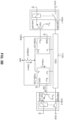
- the second current is sourced from rectifier 1600 and power source 1700, which provide a higher voltage at power supply terminal 1510 than the voltage of battery 1150.
- the second current provides charging power to battery 1150 of UAV 1100. Accordingly, when UAV 1100 lands, or is put, on conductive plate assembly 1200 of apparatus 2000, battery 1150 of UAV 1100 is charged using the second current supplied by power source 1700.
- the detector circuits include current sensors to sense whether currents flow through two or more of the detector circuits when the external power charging terminals contact two or more conductive plates.
- Selection circuit 1410-1 includes relay switch 1410-SW1 and driver circuit 1410-DR1.
- Relay switch 1410-SW1 is coupled between corresponding conductive plate 1210 and positive power-supply terminal 1510.
- Driver circuit 1410-DR1 is coupled between relay switch 1410-SW1 and current sensor 1310b-CS1.
- Driver circuit 1410-DR1 includes the NPN BJT and is coupled to the positive-voltage supply Vcc and to relay switch 1410-SW1, as shown in FIG. 5A and as described above with reference to FIG. 4A .
- the base terminal of the BJT of driver circuit 1410-DR1 ( FIG. 5A ) is coupled to the sensing output terminal (S OUT ) of current sensor 1310b-CS1.
- the positive power charging terminal at landing leg 1110 has the positive voltage sourced from the battery of UAV 1100. Because the positive power charging terminal contacts conductive plate 1210, conductive plate 1210 has the same positive voltage. When conductive plate 1210 has the positive voltage, a current 1310b-i1 flows into the current input terminal (I IN ) of current sensor 1310b-CS1 and flows out from the current output terminal (I OUT ) of current sensor 1310b-CS1.
- Current sensor 1310b-CS1 is configured to sense current 1310b-i1 and transmits a first sensing signal (e.g., current 915 in FIG. 5A ) from the sensing output terminal (S OUT ) to selection circuit 1410-1.
- a first sensing signal e.g., current 915 in FIG. 5A
- current sensor 1310b-CS2 Because the current output terminal (I OUT ) of current sensor 1310b-CS2 is coupled to conductive plate 1210 that has the positive voltage, no current flows through current sensor 1310b-CS2. As a result, current sensor 1310b-CS2 does not generate a sensing signal at its sensing output terminal (S OUT ).
- a conductive path is formed, starting from conductive plate 1210, sequentially via current sensor 1310b-CS1, resistor 1310b-R, electrically common circuit point 800, a resistor 1330b-R ( FIG. 5B ), and current sensor 1330b-CS2, to conductive plate 1230. Because conductive plates 1210 and 1230 have positive and negative voltages, respectively, a current flows from conductive plate 1210, via the conductive path, to conductive plate 1230. The current flows through current sensor 1310b-CS1 as current 1310b-i1 and through resistor 1310b-R as a current 1310b-i3, as shown in FIG. 5A .
- current sensor 1310b-CS1 When current sensor 1310b-CS1 senses current 1310b-i1, current sensor 1310b-CS1 transmits a first detection signal (e.g., current 915 in FIG. 5A ) from its sensing output (S OUT ) to driver circuit 1410-DR1 of selection circuit 1410-1.
- driver circuit 1410-DR1 In response to receiving the first detection signal (current 915), driver circuit 1410-DR1 is configured to drive and/or trigger, by a current 917 ( FIG. 5A ), relay switch 1410-SW1 to switch on to electrically connect conductive plate 1210 to positive power-supply terminal 1510.
- Detector circuit 1330b includes current sensors 1330b-CS1 and 1330b-CS2 and a resistor 1330b-R.
- Current sensors 1330b-CS1 and 1330b-CS2 each include a current input terminal I IN , a current output terminal I OUT , a ground terminal GND, and a sensing output terminal S OUT .
- the current input terminal (I IN ) of current sensor 1330b-CS1 and the current output terminal (I OUT ) of current sensor 1330b-CS2 are coupled to corresponding conductive plate 1230.
- the current output terminal (I OUT ) of current sensor 1330b-CS1 and the current input terminal (I IN ) of current sensor 1330b-CS2 are coupled to a first terminal of resistor 1330b-R.
- a second terminal of resistor 1330b-R is coupled to electrically common circuit point 800.
- the sensing output terminal (S OUT ) of current sensor 1330b-CS1 is coupled to selection circuit 1430-1.
- the sensing output terminal (S OUT ) of current sensor 1330b-CS2 is coupled to selection circuit 1430-2.
- the ground terminals GND of current sensors 1330b-CS1 and 1330b-CS2 are coupled to ground.
- Selection circuit 1430-1 includes relay switch 1430-SW1 and driver circuit 1430-DR1.
- Relay switch 1430-SW1 is coupled between corresponding conductive plate 1230 and positive power-supply terminal 1510.
- Driver circuit 1430-DR1 is coupled between relay switch 1430-SW1 and current sensor 1330b-CS1.
- Driver circuit 1430-DR1 includes the NPN BJT and is coupled to the positive-voltage supply Vcc and to relay switch 1430-SW1, as shown in FIG. 5B and as described above with reference to FIG. 4B .
- the base terminal of the BJT of driver circuit 1430-DR1 ( FIG. 5B ) is coupled to the sensing output terminal (S OUT ) of current sensor 1330b-CS1.
- Driver circuit 1430-DR1 is coupled to relay switch 1430-SW1 to provide a first switching signal to switch on relay switch 1430-SW1 to electrically connect corresponding conductive plate 1230 to positive power-supply terminal 1510 in response to receiving a first detection signal (e.g., a sensing signal or a current) from the sensing output terminal (S OUT ) of current sensor 1330b-CS1.
- a first detection signal e.g., a sensing signal or a current
- Selection circuit 1430-2 includes relay switch 1430-SW2 and driver circuit 1430-DR2.
- Relay switch 1430-SW2 is coupled between corresponding conductive plate 1230 and negative power-supply terminal 1520.
- Driver circuit 1430-DR2 is coupled between relay switch 1430-SW2 and current sensor 1330b-CS2.
- Driver circuit 1430-DR2 includes the NPN BJT and is coupled to the positive-voltage supply Vcc and to relay switch 1430-SW2, as shown in FIG. 5B and as described above with reference to FIG 4B .
- the base terminal of the BJT of driver circuit 1430-DR2 ( FIG. 5B ) is coupled to the sensing output terminal (S OUT ) of current sensor 1330b-CS2.
- Driver circuit 1430-DR2 is coupled to relay switch 1430-SW2 to provide a second switching signal to switch on relay switch 1430-SW2 to electrically connect corresponding conductive plate 1230 to negative power-supply terminal 1520 in response to receiving a second detection signal (e.g., a sensing signal or a current 936 ( FIG. 5B )) from the sensing output terminal (S OUT ) of current sensor 1330b-CS2.
- a second detection signal e.g., a sensing signal or a current 936 ( FIG. 5B )
- the negative power charging terminal at landing leg 1120 has the negative voltage sourced from the battery of UAV 1100. Because the negative power charging terminal contacts conductive plate 1230, conductive plate 1230 has the negative voltage. When conductive plate 1230 has the negative voltage, a current 1330b-i2 flows into the current input terminal (I IN ) of current sensor 1330b-CS2 and flows out from the current output terminal (I OUT ) of current sensor 1330b-CS2 to conductive plate 1230.
- Current sensor 1330b-CS2 is configured to sense current 1330b-i2 and transmits a second sensing signal (i.e., current 936 in FIG. 5B ) from its sensing output (S OUT ) to selection circuit 1430-2.
- current sensor 1330b-CS1 Because the current input terminal (I IN ) of current sensor 1330b-CS1 is coupled to conductive plate 1230 that has the negative voltage, no current flows through current sensor 1330b-CS1. As a result, current sensor 1330b-CS1 does not generate a sensing signal at its sensing output terminal (S OUT ).
- current sensor 1330b-CS2 When current sensor 1330b-CS2 senses current 1330b-i2, current sensor 1330b-CS2 transmits the second detection signal (e.g., current 936 ( FIG. 5B )) from its sensing output terminal (S OUT ) to driver circuit 1430-DR2 of selection circuit 1430-2.
- driver circuit 1430-DR2 In response to receiving the second detection signal (current 936), driver circuit 1430-DR2 is configured to drive and/or trigger, by a current 938 ( FIG. 5B ), relay switch 1430-SW2 to switch on to electrically connect conductive plate 1230 to negative power-supply terminal 1520.
- current sensor 1330b-CS1, driver circuit 1430-DR1, and relay switch 1430-SW1 are configured to operate as current sensor 1310b-CS1, driver circuit 1410-DR1, and relay switch 1410-SW1 ( FIG. 5A ) described above with reference to FIG. 5A .
- Method 600 includes detecting that a first of a plurality of conductive plates is contacted by a first of the power charging terminals based on a first current (step 610), detecting that a second of the plurality of conductive plates is contacted by a second of the power charging terminals based on a second current (step 620), electrically connecting the first conductive plate to a first of a pair of power-supply terminals (step 630), electrically connecting the second conductive plate to a second of the pair of power-supply terminals (step 640), and providing charging power to the pair of power charging terminals from the pair of power-supply terminals via the first and second conductive plates (step 650).
- Step 610 includes detecting that a first of a plurality of conductive plates is contacted by a first of the power charging terminals based on a first current.
- detector circuits 1300 of apparatus 2000 are configured to detect that conductive plate 1210 of the plurality of conductive plates of conductive plate assembly 1200 is contacted by the positive power charging terminal at landing leg 1110 based on current 1310-i1 ( FIG. 3A ).
- detector circuits 1300 are configured to detect that conductive plate 1210 of the plurality of conductive plates of conductive plate assembly 1200 is contacted by the positive power charging terminal at landing leg 1110 based on current 1310a-i1 ( FIG. 4A ) or 1310b-i1 ( FIG. 5A ).
- Step 620 includes detecting that a second of the plurality of conductive plates is contacted by a second of the power charging terminals based on a second current.
- detector circuits 1300 of apparatus 2000 are configured to detect that conductive plate 1230 of the plurality of conductive plates of conductive plate assembly 1200 is contacted by the negative power charging terminal at landing leg 1120 based on current 1330-i2 ( FIG. 3A ).
- Current 1330-i2 is sourced from current 1310-i1 via resistor 1310-R, electrically common circuit point 800, and resistor 1330-R, as shown in FIG. 3A .
- current 1310-i1 flows outwards from conductive plate 1210, via diode 1310-D1, to resistor 1310-R.
- Current 1330-i2 flows towards conductive plate 1230 from resistor 1330-R, via diode 1330-D2, as described above with reference to FIG. 3A .
- detector circuits 1300 are configured to detect that conductive plate 1230 of the plurality of conductive plates of conductive plate assembly 1200 is contacted by the negative power charging terminal at landing leg 1120 based on current 1330a-i2 ( FIG. 4B ) or 1330b-i2 ( FIG. 5B ).
- Current 1330a-i2 ( FIG. 4B ) or 1330b-i2 ( FIG. 5B ) is sourced from current 1310a-i1 ( FIG. 4A ) or 1310b-i1 ( FIG. 5A ) via resistor 1310a-R ( FIG. 4A ) or 1310b-R ( FIG. 5A ), electrically common circuit point 800, and resistor 1330a-R ( FIG. 4B ) or 1330b-R ( FIG. 5B ), as shown in FIGs. 4A and 4B , or 5A and 5B.
- FIG. 5A flows outwards from conductive plate 1210, via LED 1310a-D1 ( FIG. 4A ) or current sensor 1310b-CS1 ( FIG. 5A ), to resistor 1310a-R ( FIG. 4A ) or 1310b-R ( FIG. 5A ).
- Current 1330a-i2 ( FIG. 4B ) or 1330b-i2 ( FIG. 5B ) flows towards conductive plate 1230 from resistor 1330a-R ( FIG. 4B ) or 1330b-R ( FIG. 5B ), via LED 1330a-D2 ( FIG. 4B ) or current sensor 1330b-CS2 ( FIG. 5B ), as described above with reference to FIGs. 4A and 4B , or 5A and 5B.
- Step 630 includes electrically connecting the first conductive plate to a first of a pair of power-supply terminals.
- selection circuits 1400 of apparatus 2000 are configured to electrically connect conductive plate 1210 to positive power-supply terminal 1510 when selection circuit 1410-1 receives a detection signal, e.g., current 911, from detector circuit 1310a.
- selection circuits 1400 of apparatus 2000 are configured to electrically connect conductive plate 1210 to positive power-supply terminal 1510 when selection circuit 1410-1 receives a detection signal, e.g., current 915, from detector circuit 1310b.
- Step 640 includes electrically connecting the second conductive plate to a second of the pair of power-supply terminals.
- selection circuits 1400 of apparatus 2000 are configured to electrically connect conductive plate 1230 to negative power-supply terminal 1520 when selection circuit 1430-2 receives a detection signal, e.g., current 932, from detector circuit 1330a.
- selection circuits 1400 of apparatus 2000 are configured to electrically connect conductive plate 1230 to negative power-supply terminal 1520 when selection circuit 1430-2 receives a detection signal, e.g., current 936, from detector circuit 1330b.
- Step 650 includes providing charging power to the pair of power charging terminals from the pair of power-supply terminals via the first and second conductive plates.
- apparatus 2000 is configured to provide charging power to the pair of external power charging terminals at landing legs 1110 and 1120 of UAV 1100 from the pair of power-supply terminals 1510 and 1520 via conductive plates 1210 and 1230.
- Current 971 ( FIG. 4C ) is a charging current to battery 1150 of UAV 1100.
- a method for providing charging power may include the steps of method 600 and further include detecting that a third of the plurality of conductive plates is contacted by the first power charging terminal based on a third current and electrically connecting the third conductive plate with the first power-supply terminal.
- Providing charging power to the pair of power charging terminals of step 650 may include providing charging power to the pair of power charging terminals from the pair of power-supply terminals via the first, second, and third conductive plates.
- detector circuits 1300 of apparatus 2000 are configured to detect that conductive plates 1212 and 1242 are contacted by the positive and negative power charging terminals based on currents 1312-i1 (the first current of step 610) and 1342-i2 (the second current of step 620), respectively. Detector circuits 1300 of apparatus 2000 are also configured to detect that conductive plate 1222 of the plurality of conductive plates of conductive plate assembly 1200 is also contacted by the positive power charging terminal at landing leg 1110 based on current 1322-i1 ( FIG. 3B ).
- Selection circuits 1400 of apparatus 2000 are configured to electrically connect conductive plate 1222 with positive power-supply terminal 1510 when a selection circuit corresponding to detector circuit 1322 receives a detection signal from detector circuit 1322, similar to conductive plate 1212 as described above with reference to FIG. 3B . Because the positive power charging terminal contacts conductive plates 1212 and 1222 and the negative power charging terminal contacts conductive plate 1242, apparatus 2000 is configured to provide charging power to the power charging terminals from the pair of power-supply terminals 1510 and 1520 via conductive plates 1212, 1222, and 1242.
- current 1322-i1 flows outwards from conductive plate 1222.
- Current 1342-i2 is sourced from currents 1312-i1 and 1322-i1.
- detector circuits 1300 of apparatus 2000 are configured to detect that conductive plates 1210 and 1212 are contacted by the positive and negative power charging terminals based on currents 1310-i1 (the first current of step 610) and 1312-i2 (the second current of step 620), respectively. Detector circuits 1300 of apparatus 2000 are also configured to detect that conductive plate 1222 of the plurality of conductive plates of conductive plate assembly 1200 is contacted by the negative power charging terminal at landing leg 1120 based on current 1322-i2 ( FIG. 3C ).
- Selection circuits 1400 of apparatus 2000 are configured to electrically connect conductive plate 1222 with negative power-supply terminal 1520 when a selection circuit corresponding to detector circuit 1322 receives a detection signal from detector circuit 1322, similar to conductive plate 1212 as described above with reference to FIG. 3C . Because the positive power charging terminal contacts conductive plate 1210 and the negative power charging terminal contacts conductive plates 1212 and 1222, apparatus 2000 is configured to provide charging power to the power charging terminals from the pair of power-supply terminals 1510 and 1520 via conductive plates 1210, 1212, and 1222.
- current 1322-i2 flows towards conductive plate 1222.
- Currents 1312-i2 and 1322-i2 are sourced from current 1310-i1.
- optocoupler 1310a-OC1 is configured to generate a first detection signal (current 911) based on current 1310a-i1.
- LED 1310a-D1 of optocoupler 1310a-OC1 is configured to emit light based on current 1310a-i1.
- Phototransistor 1310a-PT1 is configured to receive the light from LED 1310a-D1 to generate the first detection signal (current 911).
- Selection circuits 1400 are configured to select positive power-supply terminal 1510 to be electrically connected to conductive plate 1210 based on the first detection signal (current 911).
- optocoupler 1330a-OC2 is configured to generate a second detection signal (current 932) based on current 1330a-i2.
- LED 1330a-D2 of optocoupler 1330a-OC2 is configured to emit light based on current 1330a-i2.
- Phototransistor 1330a-PT2 is configured to receive the light from LED 1330a-D2 to generate the second detection signal (current 932).
- Selection circuits 1400 are configured to select negative power-supply terminal 1520 to be electrically connected to conductive plate 1230 based on the second detection signal (current 932).
- a method for providing charging power may include a plurality of operations of apparatus 2000 described above with reference to FIGs. 1A-1D , 2 , 3A-3C , 4A-4C , 5A , and/or 5B.
Landscapes
- Engineering & Computer Science (AREA)
- Power Engineering (AREA)
- Transportation (AREA)
- Mechanical Engineering (AREA)
- Charge And Discharge Circuits For Batteries Or The Like (AREA)
Applications Claiming Priority (2)
| Application Number | Priority Date | Filing Date | Title |
|---|---|---|---|
| TW111122501A TWI817560B (zh) | 2022-06-16 | 2022-06-16 | 無人機充電系統 |
| US18/335,718 US20230411974A1 (en) | 2022-06-16 | 2023-06-15 | Apparatus and methods for providing charging power to an external device |
Publications (1)
| Publication Number | Publication Date |
|---|---|
| EP4293866A1 true EP4293866A1 (fr) | 2023-12-20 |
Family
ID=88758579
Family Applications (1)
| Application Number | Title | Priority Date | Filing Date |
|---|---|---|---|
| EP23179908.1A Pending EP4293866A1 (fr) | 2022-06-16 | 2023-06-16 | Appareil et procédés pour fournir une alimentation de charge à un dispositif externe |
Country Status (2)
| Country | Link |
|---|---|
| EP (1) | EP4293866A1 (fr) |
| JP (1) | JP7603749B2 (fr) |
Citations (3)
| Publication number | Priority date | Publication date | Assignee | Title |
|---|---|---|---|---|
| US20150097530A1 (en) * | 2013-10-03 | 2015-04-09 | The Boeing Company | Recharging an aircraft battery |
| US20200227870A1 (en) * | 2017-07-03 | 2020-07-16 | France Brevets | Coupling interface and method of operation |
| EP3738891A1 (fr) * | 2019-05-17 | 2020-11-18 | Fuvex Civil, SL | Plateforme d'atterrissage pour aéronefs sans pilote |
Family Cites Families (1)
| Publication number | Priority date | Publication date | Assignee | Title |
|---|---|---|---|---|
| DE102014100493A1 (de) * | 2014-01-17 | 2015-07-23 | Michele Dallachiesa | Ladevorrichtung und Verfahren zum elektrischen Laden von Batteriezellen |
-
2023
- 2023-06-16 EP EP23179908.1A patent/EP4293866A1/fr active Pending
- 2023-06-16 JP JP2023099619A patent/JP7603749B2/ja active Active
Patent Citations (3)
| Publication number | Priority date | Publication date | Assignee | Title |
|---|---|---|---|---|
| US20150097530A1 (en) * | 2013-10-03 | 2015-04-09 | The Boeing Company | Recharging an aircraft battery |
| US20200227870A1 (en) * | 2017-07-03 | 2020-07-16 | France Brevets | Coupling interface and method of operation |
| EP3738891A1 (fr) * | 2019-05-17 | 2020-11-18 | Fuvex Civil, SL | Plateforme d'atterrissage pour aéronefs sans pilote |
Also Published As
| Publication number | Publication date |
|---|---|
| JP2023184512A (ja) | 2023-12-28 |
| JP7603749B2 (ja) | 2024-12-20 |
Similar Documents
| Publication | Publication Date | Title |
|---|---|---|
| US7476988B2 (en) | Power stealing control devices | |
| CN204068303U (zh) | 一种充电系统、供电装置及飞行器 | |
| US7804195B2 (en) | Power supply system and protection method | |
| US20180366886A1 (en) | Security Control Device for Charging Trolleys Stacked Serially, Charging Device and Trolley | |
| US8797696B2 (en) | Current leakage protection circuit, power socket and electronic device using same | |
| US20120098461A1 (en) | Power supply detecting circuit | |
| CN106253639A (zh) | 正反插可识别电源装置及智能充电装置 | |
| US9966717B2 (en) | Conductive device and electrical socket for providing electric power | |
| US20230411974A1 (en) | Apparatus and methods for providing charging power to an external device | |
| CN111225472B (zh) | 温度检测和led驱动的引脚复用电路、电源芯片和引脚复用电路的工作方法 | |
| CN104111397B (zh) | 一种断电检测电路及灯具 | |
| EP4293866A1 (fr) | Appareil et procédés pour fournir une alimentation de charge à un dispositif externe | |
| US20180094778A1 (en) | Light bulb with universal serial bus port | |
| TWI882361B (zh) | 對外部設備提供充電功率的裝置和方法 | |
| CN106410928B (zh) | 充电端设备、被充电端设备、充电系统、和充电方法 | |
| EP2637281A2 (fr) | Circuit indicateur de charge | |
| US11228198B2 (en) | Charging device | |
| CN222884513U (zh) | 电源输入电路和显示屏 | |
| US9553464B2 (en) | In-vehicle-mounted charging device | |
| KR20130061741A (ko) | 축전 모듈의 과전압 검출 장치 | |
| TWI517519B (zh) | 識別適配器種類的充電裝置及其方法 | |
| US9510412B2 (en) | Lighting system | |
| US8233296B2 (en) | Front-end circuit of power converter | |
| CN217135177U (zh) | 一种充电电路及电子产品 | |
| US7859873B2 (en) | Operation control circuit |
Legal Events
| Date | Code | Title | Description |
|---|---|---|---|
| PUAI | Public reference made under article 153(3) epc to a published international application that has entered the european phase |
Free format text: ORIGINAL CODE: 0009012 |
|
| STAA | Information on the status of an ep patent application or granted ep patent |
Free format text: STATUS: THE APPLICATION HAS BEEN PUBLISHED |
|
| AK | Designated contracting states |
Kind code of ref document: A1 Designated state(s): AL AT BE BG CH CY CZ DE DK EE ES FI FR GB GR HR HU IE IS IT LI LT LU LV MC ME MK MT NL NO PL PT RO RS SE SI SK SM TR |
|
| STAA | Information on the status of an ep patent application or granted ep patent |
Free format text: STATUS: REQUEST FOR EXAMINATION WAS MADE |
|
| 17P | Request for examination filed |
Effective date: 20240620 |
|
| RBV | Designated contracting states (corrected) |
Designated state(s): AL AT BE BG CH CY CZ DE DK EE ES FI FR GB GR HR HU IE IS IT LI LT LU LV MC ME MK MT NL NO PL PT RO RS SE SI SK SM TR |
|
| STAA | Information on the status of an ep patent application or granted ep patent |
Free format text: STATUS: EXAMINATION IS IN PROGRESS |
|
| 17Q | First examination report despatched |
Effective date: 20251022 |