EP4297065A1 - Pixelanordnungsstruktur, anzeigetafel und anzeigevorrichtung - Google Patents
Pixelanordnungsstruktur, anzeigetafel und anzeigevorrichtung Download PDFInfo
- Publication number
- EP4297065A1 EP4297065A1 EP22905942.3A EP22905942A EP4297065A1 EP 4297065 A1 EP4297065 A1 EP 4297065A1 EP 22905942 A EP22905942 A EP 22905942A EP 4297065 A1 EP4297065 A1 EP 4297065A1
- Authority
- EP
- European Patent Office
- Prior art keywords
- pixel
- sub
- pixels
- arrangement structure
- adjacent
- Prior art date
- Legal status (The legal status is an assumption and is not a legal conclusion. Google has not performed a legal analysis and makes no representation as to the accuracy of the status listed.)
- Pending
Links
- 239000000463 material Substances 0.000 abstract description 17
- 239000003086 colorant Substances 0.000 abstract description 16
- 239000010410 layer Substances 0.000 description 38
- 238000000151 deposition Methods 0.000 description 16
- 230000001965 increasing effect Effects 0.000 description 16
- 230000008021 deposition Effects 0.000 description 14
- 238000004519 manufacturing process Methods 0.000 description 13
- 238000002156 mixing Methods 0.000 description 13
- 238000007740 vapor deposition Methods 0.000 description 10
- 230000000694 effects Effects 0.000 description 9
- 238000005516 engineering process Methods 0.000 description 9
- 238000000034 method Methods 0.000 description 9
- 230000008569 process Effects 0.000 description 9
- 229910001111 Fine metal Inorganic materials 0.000 description 8
- 239000000758 substrate Substances 0.000 description 7
- 238000002347 injection Methods 0.000 description 6
- 239000007924 injection Substances 0.000 description 6
- 230000008859 change Effects 0.000 description 4
- 230000007547 defect Effects 0.000 description 4
- 230000001788 irregular Effects 0.000 description 4
- 230000011218 segmentation Effects 0.000 description 4
- 230000000007 visual effect Effects 0.000 description 4
- 230000003247 decreasing effect Effects 0.000 description 3
- 238000005019 vapor deposition process Methods 0.000 description 3
- 238000005452 bending Methods 0.000 description 2
- 230000008901 benefit Effects 0.000 description 2
- 230000000295 complement effect Effects 0.000 description 2
- 230000002708 enhancing effect Effects 0.000 description 2
- 230000005525 hole transport Effects 0.000 description 2
- 206010049155 Visual brightness Diseases 0.000 description 1
- 238000009825 accumulation Methods 0.000 description 1
- 230000003321 amplification Effects 0.000 description 1
- 238000013473 artificial intelligence Methods 0.000 description 1
- 230000009286 beneficial effect Effects 0.000 description 1
- 239000000969 carrier Substances 0.000 description 1
- 230000007423 decrease Effects 0.000 description 1
- 230000002950 deficient Effects 0.000 description 1
- 238000005137 deposition process Methods 0.000 description 1
- 229910003460 diamond Inorganic materials 0.000 description 1
- 239000010432 diamond Substances 0.000 description 1
- 238000005530 etching Methods 0.000 description 1
- 238000001704 evaporation Methods 0.000 description 1
- 239000011521 glass Substances 0.000 description 1
- 238000010438 heat treatment Methods 0.000 description 1
- 239000002346 layers by function Substances 0.000 description 1
- 239000004973 liquid crystal related substance Substances 0.000 description 1
- 239000002184 metal Substances 0.000 description 1
- 239000000203 mixture Substances 0.000 description 1
- 238000012986 modification Methods 0.000 description 1
- 230000004048 modification Effects 0.000 description 1
- 239000011664 nicotinic acid Substances 0.000 description 1
- 238000003199 nucleic acid amplification method Methods 0.000 description 1
- 230000009467 reduction Effects 0.000 description 1
- 239000000243 solution Substances 0.000 description 1
- 238000009827 uniform distribution Methods 0.000 description 1
Images

Classifications
-
- H—ELECTRICITY
- H10—SEMICONDUCTOR DEVICES; ELECTRIC SOLID-STATE DEVICES NOT OTHERWISE PROVIDED FOR
- H10K—ORGANIC ELECTRIC SOLID-STATE DEVICES
- H10K59/00—Integrated devices, or assemblies of multiple devices, comprising at least one organic light-emitting element covered by group H10K50/00
- H10K59/30—Devices specially adapted for multicolour light emission
- H10K59/35—Devices specially adapted for multicolour light emission comprising red-green-blue [RGB] subpixels
-
- H—ELECTRICITY
- H10—SEMICONDUCTOR DEVICES; ELECTRIC SOLID-STATE DEVICES NOT OTHERWISE PROVIDED FOR
- H10K—ORGANIC ELECTRIC SOLID-STATE DEVICES
- H10K59/00—Integrated devices, or assemblies of multiple devices, comprising at least one organic light-emitting element covered by group H10K50/00
- H10K59/30—Devices specially adapted for multicolour light emission
- H10K59/35—Devices specially adapted for multicolour light emission comprising red-green-blue [RGB] subpixels
- H10K59/351—Devices specially adapted for multicolour light emission comprising red-green-blue [RGB] subpixels comprising more than three subpixels, e.g. red-green-blue-white [RGBW]
-
- H—ELECTRICITY
- H10—SEMICONDUCTOR DEVICES; ELECTRIC SOLID-STATE DEVICES NOT OTHERWISE PROVIDED FOR
- H10K—ORGANIC ELECTRIC SOLID-STATE DEVICES
- H10K59/00—Integrated devices, or assemblies of multiple devices, comprising at least one organic light-emitting element covered by group H10K50/00
- H10K59/30—Devices specially adapted for multicolour light emission
- H10K59/35—Devices specially adapted for multicolour light emission comprising red-green-blue [RGB] subpixels
- H10K59/352—Devices specially adapted for multicolour light emission comprising red-green-blue [RGB] subpixels the areas of the RGB subpixels being different
-
- H—ELECTRICITY
- H10—SEMICONDUCTOR DEVICES; ELECTRIC SOLID-STATE DEVICES NOT OTHERWISE PROVIDED FOR
- H10K—ORGANIC ELECTRIC SOLID-STATE DEVICES
- H10K59/00—Integrated devices, or assemblies of multiple devices, comprising at least one organic light-emitting element covered by group H10K50/00
- H10K59/30—Devices specially adapted for multicolour light emission
- H10K59/35—Devices specially adapted for multicolour light emission comprising red-green-blue [RGB] subpixels
- H10K59/353—Devices specially adapted for multicolour light emission comprising red-green-blue [RGB] subpixels characterised by the geometrical arrangement of the RGB subpixels
Definitions
- the present application relates to the field of display technologies, and in particular to a pixel arrangement structure, a display panel, and a display apparatus.
- OLED Organic light-emitting diode
- RGB red
- B blue
- G green
- the existing pixel arrangement structure still has the problem that the display effect of the OLED device would be affected by the properties of the organic light-emitting materials.
- a pixel arrangement structure comprising at least one first sub-pixel having centers coincident with vertexes of a first virtual quadrilateral, a second sub-pixel located in the first virtual quadrilateral and spaced apart from the first sub-pixels, and a third sub-pixel located in the first virtual quadrilateral and spaced apart from the first sub-pixels and from the second sub-pixel.
- the second sub-pixel has a larger opening area than the first sub-pixel or the third sub-pixel.
- each pixel can display all colors, and the display details are good.
- each first sub-pixel is surrounded by the second and third sub-pixels, thereby preventing the color deviation.
- the opening area of the second sub-pixel is larger than the opening area of the first sub-pixel or the third sub-pixel, which can reduce display color deviation caused by the difference in the decay rates of the organic light-emitting materials emitting different color lights to a certain extent.
- a minimum distance between two adjacent first sub-pixels in the first direction is a first distance X.
- a minimum distance between two adjacent first sub-pixels in the second direction is a second distance Y.
- the first sub-pixel, the second sub-pixel, and the third sub-pixel each have a polygon shape.
- the first sub-pixel, the second sub-pixel, and the third sub-pixel each have a quadrilateral shape.
- a distance between two first pixel edges of the second sub-pixel and the third sub-pixel in the same first virtual quadrilateral is the fourth length.
- a distance between two second pixel edges of adjacent second sub-pixel and third sub-pixel in two adjacent first virtual quadrilaterals in the second direction is the fifth length.
- the fourth length is equal to the fifth length.
- At least one pixel edge of the first sub-pixel is configured to be concave toward the center of the first sub-pixel.
- the pixel edge of the first sub-pixel which is concave toward the center of the first sub-pixel is in a form of a curved line or a bending line.
- four second sub-pixels respectively located in any four first virtual quadrilaterals adjacent to each other in the first direction and the second direction have centers coincident with vertexes of a second virtual quadrilateral.
- Four third sub-pixels respectively located in these four first virtual quadrilaterals adjacent to each other have centers coincident with vertexes of a third virtual quadrilateral.
- An area of the second virtual quadrilateral is equal to an area of the third virtual quadrilateral.
- the first virtual quadrilateral, the second virtual quadrilateral, and the third virtual quadrilateral are equilateral quadrilaterals with a same edge length.
- the first sub-pixel emits green lights
- the second sub-pixel emits blue lights
- the third sub-pixel emits red lights
- Pixels Per Inch also known as pixel density, which refers to the number of pixels per inch.
- FHD resolution with a 5-inch size has a pixel density of 441PPI. Therefore, with a fixed size of the display panel, the higher the resolution, the higher the PPI may be.
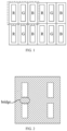
- the conventional Real-RGB pixel arrangement is mostly adopted. As shown in FIG. 1 , the size ratio of the sub-pixels in the conventional Real-RGB pixel arrangement is 1:1:1. That is, one square pixel is divided into three equal parts which are arranged side by side and assigned with different colors to constitute a color pixel. As such, pixels with high independence are achieved, and each pixel can display all colors, resulting in better display details.
- OLED organic light-emitting diode
- a pixel-driving circuit is required to be connected to the sub-pixel of the OLED display, in order to provide the electric current for the OLED device to enable the OLED device to emit lights.
- the OLED device includes at least an anode, a cathode, and an organic light-emitting material layer located between the anode and the cathode. Taking the top-emitting OLED display panel as an example, due to the poor stability of the organic light-emitting material, conventional etching processes cannot be used to pattern the organic light-emitting material layer.
- the mask used for vapor-deposition of the organic light-emitting material layers of various sub-pixels is a fine metal mask (FMM), also known as a fine mask. It is very difficult to produce a fine metal mask, and it becomes more difficult and costly especially as the number of openings on a fine metal mask is increasingly more with the resolution of the display product which becomes higher and higher. In addition, defects in the fine metal mask can cause color mixing and other defects in an OLED device, and the more times the fine metal mask is used, the more likely it is to produce a defective product, thereby reducing the yield of product.
- FMM fine metal mask
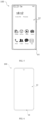
- the display panel in at least one embodiment of the present application includes a display region 12 and a non-display region 14.
- the display panel displays an image through a plurality of sub-pixels arranged in the display region 12.
- the display region 12 can be rectangular, and the non-display region 14 is configured to surround the display region 12.
- the shapes and the arrangements of the display region 12 and the non-display region 14 are not limited to the above embodiments.
- the display region 12 when the display panel is used in a wearable apparatus worn by a user, the display region 12 can have a circular shape like a wristwatch.
- the display region 12 and the non-display region 14 can be circular, polygonal, or other shapes.
- the display region 12 is provided with a plurality of sub-pixels for emitting lights in different colors.
- the light-emitting unit 40 in the present application can specifically include an electron injection layer, an electron transport layer, an organic light-emitting layer, a hole transport layer, a hole injection layer, and the like which are stacked with each other.
- the electron injection layer, the electron transport layer, the hole transport layer, or the hole injection layer can be an entire layer structure formed using a common metal mask (CMM).
- CCM common metal mask
- the electron injection layers of the plurality of sub-pixels are connected to each other to collectively form a continuous and entire layer structure.
- the organic light-emitting layer is a patterned layer structure corresponding to each sub-pixels, i.e., a film/layer formed using a fine metal mask (FMM).
- FMM fine metal mask
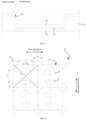
- the first sub-pixels 22 can have the centers coincident with the vertexes of the first virtual quadrilaterals M in order to ensure the uniform distribution of the sub-pixels.
- the centers of the sub-pixels may also have an offset within a tolerance range from the vertexes of the first virtual quadrilaterals M. Therefore, when referring to that the centers of the sub-pixels coincide with the vertexes of the virtual quadrilaterals, it should not be understood as requiring the centers of the first sub-pixels 22 to be 100% coincident with the vertexes of the first virtual quadrilaterals M, which may limit the scope of protection.
- lights in different colors have different wavelengths.
- the shorter the wavelength the higher the energy of the light.
- High-energy light tends to cause the decay of the organic light-emitting material, so that the sub-pixel emitting high-energy lights is more prone to decay.
- the wavelength of the blue light is shorter than those of the red light and the green light, so the blue light has higher energy, and the organic light-emitting material emitting the blue light is more prone to decay, as a result, the lights emitted by the sub-pixels tend to be reddish, causing the phenomenon of white light color deviation .
- the pixel arrangement structure 20 directly determines the display effect.
- the sub-pixels are usually arranged as evenly as possible in the row and column directions according to a certain rule.
- the color deviation cannot be completely avoided.
- a line connecting centers of the second sub-pixel 24 and the third sub-pixel 26 located in the first virtual quadrilateral M passes through the center of the first virtual quadrilateral M.
- the distance between the pixel edges of two adjacent sub-pixels is larger than the sum of the deposition margins for vapordepositing the two adjacent sub-pixels.
- the projected contour boundaries of the deposition apertures of the mask on the display substrate corresponding to the two adjacent sub-pixels are spaced apart from each other.
- the adjacent pixel edges of the two adjacent sub-pixels are parallel to each other.
- a dividing line between the two adjacent sub-pixels is the perpendicular bisector of the perpendicular line between the adjacent pixel edges of the two adjacent sub-pixels.
- angles of the pixel opening corresponding to the vertex angles opposite to each other in the stretching direction can provide some guidance for the inward shrinking to prevent the mask from folding when stretching, which can cause the change in the positions of the pixel openings and positions for vapor depositing sub-pixels and thus the color mixing with other sub-pixels.
- angles of the deposition opening corresponding to another pair of vertex angles of the sub-pixel in the non-stretching direction e.g., the second direction, can also counteract the inward shrinking to further prevent the mask from folding when stretching.
- the deposition openings of the mask are uniformly stressed during the stretching of the mask, avoiding large deformation of the pixel openings due to uneven stress which may affect the vapor deposition of the organic light-emitting layers of the sub-pixels.
- the shapes of the sub-pixels can be more regular, which is conducive to the uniform arrangement of the sub-pixels and improves the display quality.
- the geometric center of the sub-pixel is usually its visual focus.
- the shape of the first sub-pixel 22 as being defined by pixel edges that are not parallel to the first direction or the second direction, and configuring any two adjacent first sub-pixels 22 to be symmetrically placed about the extension of the line connecting the centers thereof, the widths of the first sub-pixel 22 in the first and second directions can be continuously and uniformly changed in a regular manner, which allows a distance between the visual focuses of two adjacent first sub-pixels 22 to be in a reasonable range, so that the human eye can accurately distinguish two adjacent sub-pixels with the same color, ensuring that the visual resolution of the display panel is the same as its physical resolution, the displayed image on the display panel is delicate and clear, and the display panel has good display effect.
- the size of the deposition openings of the mask used in the vaper deposition process corresponds to the size of the organic light-emitting functional layer.
- the vertex angle of the first sub-pixel 22 is too small, the size of the corresponding angle of the deposition opening of the mask is small, which makes the manufacture of the mask difficult.
- a small process error will cause large change in the above-mentioned vertex angle. Therefore, a small vertex angle of the first sub-pixel 22 would increase the difficulty of manufacturing the display panel.
- the vertex angle of the first sub-pixel 22 is in a range of 80° to 100°, so that it is less difficult to manufacture the mask for the organic light-emitting layers in the first sub-pixels 22, and to manufacture a display panel.
- each sub-pixel of the second sub-pixels 24 and the third sub-pixels 26 has a pixel edge that is not parallel to the first direction and the second direction.
- the pixel edges of the second sub-pixel 24 and the third sub-pixel 26 that are not parallel to the first direction or the second direction are opposite to the adjacent pixel edge of the adjacent first sub-pixel 22. For example, as shown in FIG.
- the second sub-pixel 24 and the third sub-pixel 26 are set to have non-equilateral quadrilateral shapes.
- each of the second sub-pixel 24 and the third sub-pixel 26 has a first pixel edges (not shown) and a second pixel edge (not shown) opposite to each other.
- the length of the first pixel edge is larger than the length of the second pixel edge of the same sub-pixel.
- the two first pixel edges of the second sub-pixel 24 and the third sub-pixel 26 are adjacent and parallel to each other.
- Two second pixel edges in two adjacent first virtual quadrilaterals M in the second direction are adjacent and parallel to each other.
- Each of the second sub-pixel 24 and the third sub-pixel 26 also has a third pixel edge and a fourth pixel edge connecting the first pixel edge and the second pixel edge.
- the third pixel edge and the fourth pixel edge are set at an angle with the first direction or the second direction.
- the first pixel edge and the second pixel edge of the second sub-pixel 24 and the third sub-pixel 26 are both parallel to the first direction. In this way, not only the opening areas of the second sub-pixel 24 and the third sub-pixel 26 are ensured in order to obtain higher resolution under the same display panel size, but also the risk of deposition color mixing between different color sub-pixels is reduced. Under the aforementioned constraints, the maximum aperture rate of each sub-pixel in the pixel arrangement structure 20 is achieved while satisfying the extreme process conditions.
- the second pixel edge of the second sub-pixel 24 has a first length L1.
- L2 (1.5 to 2.5) L1.
- a line passing through the vertexes of another pair of opposite vertex angles of the first sub-pixel 22 also passes through the center of this first sub-pixel 22. Then, the size of the first sub-pixel 22 in the first direction gradually increases and then gradually decreases along the second direction, and the maximum size of the first sub-pixel 22 in the first direction is the distance between the vertexes of the first vertex angle and the second vertex angle opposite to each other of the first sub-pixel 22.
- the second sub-pixel 24 and the third sub-pixel 26 are at least partially complementary with the two first sub-pixels 22, thereby reducing the area of the blank region between adjacent sub-pixels and increasing the aperture rate of the display panel, it also needs to ensure that the second sub-pixel 24 and the third sub-pixel 26 are evenly spaced from the adjacent first sub-pixel 22.
- the lengths of the second pixel edges of the second sub-pixel 24 and the third sub-pixel 26 would affect the shapes and sizes of the second sub-pixel 24 and the third sub-pixel 26, when other parameters such as the area of the display panel, the resolution, PPI, and the aperture rate are fixed.
- the shape and the size of each sub-pixel are more reasonable, which is conducive to the uniform arrangement of sub-pixels, thereby improving the display quality, and also reduces the difficulty of stretching the mask.
- the aperture rate of each sub-pixel in the pixel arrangement structure 20 is maximized under the conditions of satisfying the extreme process.
- the second pixel edge of the third sub-pixel 26 has a third length L3, and the second length L2 is set to be 1.5 to 2.5 times the third length L3.
- the length of the first pixel edge of the second sub-pixel 24 is greater than the length of the first pixel edge of the third sub-pixel 26, and the length of the second pixel edge of the second sub-pixel 24 is greater than the length of the second pixel edge of the third sub-pixel 26. In this way, the second sub-pixel 24 has a larger opening area than the first sub-pixel 22 or the third sub-pixel 26.
- each of the second sub-pixel 24 and the third sub-pixel 26 located in the same first virtual quadrilateral M is configured to be symmetrically placed about the extension of the line connecting centers of the second sub-pixel 24 and the third sub-pixel 26. This ensures that the shapes of the sub-pixels are more regular, which is conducive to the uniform arrangement of sub-pixels and improves the display uniformity.
- a distance between the two first pixel edges of the second sub-pixel 24 and the third sub-pixel 26 is the fourth length.
- a distance between the two second pixel edges of adjacent second sub-pixels 24 and third sub-pixels 26 is the fifth length.
- the fourth length is equal to the fifth length, which is conducive to the uniform arrangement of sub-pixels and improves the display uniformity.
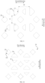
- FIG. 9 shows a schematic arrangement view of a pixel arrangement structure in another embodiment of the present application.
- the second sub-pixel 24 has a pixel edge extending along the first direction and a vertex angle ⁇ opposite to this pixel edge in the second direction.
- Parts of two edges of the vertex angle ⁇ which are supposed to extend to and intersect at a vertex of the vertex angle ⁇ , form a straight line segment to cause the vertex angle ⁇ to be a flat chamfer, wherein the straight line segment is parallel to the first direction.
- parts of the two edges of the vertex angle ⁇ which are supposed to extend to and intersect at the vertex of the vertex angle ⁇ , form an arc line segment to cause the vertex angle ⁇ to be a round chamfer, wherein a tangent of the arc line segment is parallel to the first direction.
- the difficulty of manufacturing the mask and the vapor deposition are reduced.
- a distance H between two second sub-pixels in two adjacent first virtual quadrilaterals M in the second direction is increased, further reducing the difficulty of manufacturing the mask and the vapor deposition.
- two adjacent second sub-pixels 24 in the first direction respectively have two opposite vertex angles.
- two adjacent second sub-pixels 24 in the first direction respectively have a third vertex angle ⁇ and a fourth vertex angle ⁇ opposite to each other.
- Parts of two edges of each of the two opposite vertex angles which are supposed to extend to and intersect at a vertex of the vertex angle, form a straight line segment to cause the vertex angle to be a flat chamfer, wherein the straight line is inclined relative to the first direction.
- parts of two edges of each of the two opposite vertex angles i.e., the third vertex angle ⁇ and the fourth vertex angle ⁇ , which are supposed to extend to and intersect at a vertex of the vertex angle, can also form an arc line segment to cause the vertex angle to be a round chamfer, wherein a tangent of the arch line segment is inclined relative to the first direction.
- the gap between the organic light-emitting layers of two adjacent second sub-pixels 24 in the first direction can also be increased, effectively decreasing the color mixing risk of the organic light-emitting layers at the vertex angle, and making the manufacture easy.
- round chamfer in the present application refers to an angle formed by rounding an angle of a polygon
- flat chamfer refers to an angle formed by replacing the arc line segment of the round chamfer with a straight line segment.
- the jaggedness of the boundary region of the display region 12 is also a factor affecting the display quality.
- the present inventors have found that if the sub-pixels in different rows form a stepped shape along the extension direction of the boundary region, then the jaggedness of the image at the boundary region of the display panel would be more severe when displaying images, thereby affecting the display effect of the display panel. Therefore, the shape of the first sub-pixel 22 is configured to be defined by pixel edges that are not parallel to the first and second directions, and the second sub-pixel 24 and the third sub-pixel 26 have pixel edges that are not parallel to the first and second directions.
- FIG. 10 shows a schematic arrangement view of a pixel arrangement structure in another embodiment of the present application.
- At least one pixel edge 222 of the first sub-pixel 22 is configured to be concave toward the center of the first sub-pixel 22.
- the first sub-pixels 22, the second sub-pixels 24, and the third sub-pixels 26 can be arranged compactly, minimizing the distance between adjacent sub-pixels.
- the distance between the first sub-pixel 22 and the adjacent second sub-pixel 24 or the adjacent third sub-pixel 26 can be further reduced, so that under the same resolution, the opening areas of the sub-pixels are increased, the aperture ratio is improved, the driving current for the sub-pixels is decreased, and the life of the display panel is increased.
- the display apparatus 100 can be applied in various fields such as mobile terminal, bionic electronics, electronic skin, wearable equipment, automotive equipment, Internet of Things (IoT) equipment, and artificial intelligence (AI) equipment.
- the display apparatus 100 can be a digital apparatus such as a mobile phone, a tablet, a handheld computer, iPod, or a smartwatch.
Landscapes
- Electroluminescent Light Sources (AREA)
Applications Claiming Priority (2)
| Application Number | Priority Date | Filing Date | Title |
|---|---|---|---|
| CN202111518173.9A CN114156332B (zh) | 2021-12-13 | 2021-12-13 | 像素排布结构、显示面板和显示装置 |
| PCT/CN2022/115438 WO2023109186A1 (zh) | 2021-12-13 | 2022-08-29 | 像素排布结构、显示面板和显示装置 |
Publications (2)
| Publication Number | Publication Date |
|---|---|
| EP4297065A1 true EP4297065A1 (de) | 2023-12-27 |
| EP4297065A4 EP4297065A4 (de) | 2024-10-16 |
Family
ID=80450404
Family Applications (1)
| Application Number | Title | Priority Date | Filing Date |
|---|---|---|---|
| EP22905942.3A Pending EP4297065A4 (de) | 2021-12-13 | 2022-08-29 | Pixelanordnungsstruktur, anzeigetafel und anzeigevorrichtung |
Country Status (5)
| Country | Link |
|---|---|
| US (1) | US20240016020A1 (de) |
| EP (1) | EP4297065A4 (de) |
| KR (1) | KR102841037B1 (de) |
| CN (1) | CN114156332B (de) |
| WO (1) | WO2023109186A1 (de) |
Families Citing this family (3)
| Publication number | Priority date | Publication date | Assignee | Title |
|---|---|---|---|---|
| CN114156332B (zh) * | 2021-12-13 | 2025-12-23 | 昆山国显光电有限公司 | 像素排布结构、显示面板和显示装置 |
| CN117119850A (zh) * | 2023-08-31 | 2023-11-24 | 惠科股份有限公司 | 像素结构以及显示基板 |
| CN117452698A (zh) * | 2023-11-15 | 2024-01-26 | 武汉华星光电半导体显示技术有限公司 | 彩膜基板以及显示装置 |
Family Cites Families (35)
| Publication number | Priority date | Publication date | Assignee | Title |
|---|---|---|---|---|
| US7274383B1 (en) * | 2000-07-28 | 2007-09-25 | Clairvoyante, Inc | Arrangement of color pixels for full color imaging devices with simplified addressing |
| US20040246426A1 (en) * | 2003-06-03 | 2004-12-09 | Pei-Chang Wang | Color pixel arrangement of display |
| US20080001525A1 (en) * | 2006-06-30 | 2008-01-03 | Au Optronics Corporation | Arrangements of color pixels for full color OLED |
| KR101015332B1 (ko) * | 2009-07-14 | 2011-02-15 | 삼성모바일디스플레이주식회사 | 유기전계발광 표시장치의 화소배열구조 |
| KR20110129531A (ko) * | 2010-05-26 | 2011-12-02 | 삼성모바일디스플레이주식회사 | 유기전계발광 표시장치의 화소배열구조 |
| KR101189025B1 (ko) * | 2010-05-31 | 2012-10-08 | 삼성디스플레이 주식회사 | 유기전계발광 표시장치의 화소배열구조 |
| DE102011053000B4 (de) * | 2010-08-27 | 2017-08-17 | Lg Display Co., Ltd. | Organische elektrolumineszente Vorrichtung |
| KR101257734B1 (ko) * | 2010-09-08 | 2013-04-24 | 엘지디스플레이 주식회사 | 유기전계발광 표시장치 |
| KR101328979B1 (ko) * | 2011-06-30 | 2013-11-13 | 삼성디스플레이 주식회사 | 유기 발광 표시장치 |
| WO2014014032A1 (ja) * | 2012-07-19 | 2014-01-23 | シャープ株式会社 | 液晶表示装置 |
| KR101427593B1 (ko) * | 2013-04-26 | 2014-08-07 | 삼성디스플레이 주식회사 | 유기 발광 표시 장치 |
| CN105552099A (zh) * | 2014-10-29 | 2016-05-04 | 上海和辉光电有限公司 | 一种oled像素排列结构 |
| CN104465714B (zh) * | 2014-12-30 | 2017-04-26 | 京东方科技集团股份有限公司 | 一种像素结构及其显示方法、显示装置 |
| CN104681594B (zh) * | 2015-03-11 | 2018-01-12 | 京东方科技集团股份有限公司 | 像素排列结构和显示装置 |
| CN106486514B (zh) * | 2015-08-31 | 2023-12-01 | 昆山国显光电有限公司 | 像素结构以及oled显示面板 |
| US11233096B2 (en) * | 2016-02-18 | 2022-01-25 | Boe Technology Group Co., Ltd. | Pixel arrangement structure and driving method thereof, display substrate and display device |
| CN110137213B (zh) * | 2018-02-09 | 2025-03-25 | 京东方科技集团股份有限公司 | 像素排列结构及其显示方法、显示基板 |
| CN109994504A (zh) * | 2018-01-02 | 2019-07-09 | 京东方科技集团股份有限公司 | 一种像素排布结构及相关装置 |
| CN110137210B (zh) * | 2018-02-09 | 2025-06-27 | 京东方科技集团股份有限公司 | 一种像素排布结构及相关装置 |
| CN108364983A (zh) * | 2018-02-01 | 2018-08-03 | 武汉华星光电半导体显示技术有限公司 | 像素排列结构 |
| CN110137208A (zh) * | 2018-02-09 | 2019-08-16 | 京东方科技集团股份有限公司 | 一种像素排布结构、高精度金属掩模板及显示装置 |
| CN110137206B (zh) * | 2018-02-09 | 2025-01-21 | 京东方科技集团股份有限公司 | 一种像素排布结构及相关装置 |
| US11574960B2 (en) * | 2018-02-09 | 2023-02-07 | Boe Technology Group Co., Ltd. | Pixel arrangement structure, display substrate, display device and mask plate group |
| CN110137209A (zh) * | 2018-02-09 | 2019-08-16 | 京东方科技集团股份有限公司 | 一种像素排布结构、高精度金属掩模板及显示装置 |
| CN109935617B (zh) * | 2018-11-30 | 2024-04-05 | 京东方科技集团股份有限公司 | 像素排列结构、显示基板以及掩模板组 |
| CN112768500B (zh) * | 2018-12-13 | 2023-10-31 | 昆山国显光电有限公司 | 像素排列结构、显示面板及显示装置 |
| CN110277436A (zh) * | 2019-06-28 | 2019-09-24 | 云谷(固安)科技有限公司 | 像素排列结构及显示面板 |
| CN110335892B (zh) * | 2019-07-15 | 2021-03-26 | 云谷(固安)科技有限公司 | 像素排布结构、显示面板及显示装置 |
| CN110491911A (zh) * | 2019-07-31 | 2019-11-22 | 云谷(固安)科技有限公司 | 像素排列结构和显示面板 |
| CN110444569A (zh) * | 2019-08-02 | 2019-11-12 | 云谷(固安)科技有限公司 | 像素排列结构及显示面板 |
| CN110459574A (zh) * | 2019-08-20 | 2019-11-15 | 武汉天马微电子有限公司 | 一种显示面板及显示装置 |
| CN110993665B (zh) * | 2019-12-06 | 2022-04-29 | 云谷(固安)科技有限公司 | 一种像素排列结构及显示面板 |
| CN111415961B (zh) * | 2020-03-30 | 2022-04-26 | 深圳市华星光电半导体显示技术有限公司 | 像素排列结构、有机电致发光器件及显示装置 |
| CN113437122B (zh) * | 2021-06-17 | 2022-09-23 | 合肥维信诺科技有限公司 | 像素排布结构、掩膜组件及显示面板 |
| CN114156332B (zh) * | 2021-12-13 | 2025-12-23 | 昆山国显光电有限公司 | 像素排布结构、显示面板和显示装置 |
-
2021
- 2021-12-13 CN CN202111518173.9A patent/CN114156332B/zh active Active
-
2022
- 2022-08-29 WO PCT/CN2022/115438 patent/WO2023109186A1/zh not_active Ceased
- 2022-08-29 EP EP22905942.3A patent/EP4297065A4/de active Pending
- 2022-08-29 KR KR1020237031450A patent/KR102841037B1/ko active Active
-
2023
- 2023-09-22 US US18/472,499 patent/US20240016020A1/en active Pending
Also Published As
| Publication number | Publication date |
|---|---|
| WO2023109186A1 (zh) | 2023-06-22 |
| CN114156332A (zh) | 2022-03-08 |
| EP4297065A4 (de) | 2024-10-16 |
| US20240016020A1 (en) | 2024-01-11 |
| KR20230140592A (ko) | 2023-10-06 |
| CN114156332B (zh) | 2025-12-23 |
| KR102841037B1 (ko) | 2025-07-31 |
Similar Documents
| Publication | Publication Date | Title |
|---|---|---|
| CN112436029B (zh) | 像素排布结构、显示面板及显示装置 | |
| US20240016020A1 (en) | Pixel arrangement structure, display panel, and display apparatus | |
| US11342385B2 (en) | Pixel arrangement structure, display substrate, display device, and mask plate group | |
| US12329010B1 (en) | Display panels and display devices | |
| US10680041B2 (en) | Pixel arrangement structure and related apparatus | |
| CN112436031B (zh) | 像素排布结构、显示面板及显示装置 | |
| US12598884B2 (en) | Display panel and display device | |
| KR102904709B1 (ko) | 픽셀 배열 구조, 디스플레이 패널 및 디스플레이 장치 | |
| US20190355795A1 (en) | Pixel structure and display panel having the same | |
| US12490617B2 (en) | Pixel arrangement structure and display panel | |
| CN114122093B (zh) | 像素排布结构、显示面板和显示装置 | |
| US20210335909A1 (en) | Pixel arrangement structure, display method and preparing method of pixel arrangement structure, and display substrate | |
| US11647653B2 (en) | OLED display panel | |
| US20250359431A1 (en) | Array substrate and display device | |
| US11195882B2 (en) | Pixel arrangement structure, display substrate and display device | |
| US20260130084A1 (en) | Pixel arrangement structure and display device | |
| CN115332298B (zh) | 显示像素排布结构、显示面板及显示面板的制备方法 | |
| CN119744577A (zh) | 像素排列结构和显示装置 | |
| CN118647234A (zh) | 像素排列结构、显示面板及显示装置 | |
| JPH02165596A (ja) | ドツトマトリツクス型薄膜el素子 |
Legal Events
| Date | Code | Title | Description |
|---|---|---|---|
| STAA | Information on the status of an ep patent application or granted ep patent |
Free format text: STATUS: THE INTERNATIONAL PUBLICATION HAS BEEN MADE |
|
| PUAI | Public reference made under article 153(3) epc to a published international application that has entered the european phase |
Free format text: ORIGINAL CODE: 0009012 |
|
| STAA | Information on the status of an ep patent application or granted ep patent |
Free format text: STATUS: REQUEST FOR EXAMINATION WAS MADE |
|
| 17P | Request for examination filed |
Effective date: 20230920 |
|
| AK | Designated contracting states |
Kind code of ref document: A1 Designated state(s): AL AT BE BG CH CY CZ DE DK EE ES FI FR GB GR HR HU IE IS IT LI LT LU LV MC MK MT NL NO PL PT RO RS SE SI SK SM TR |
|
| REG | Reference to a national code |
Ref country code: DE Ref legal event code: R079 Free format text: PREVIOUS MAIN CLASS: H99Z9999999999 Ipc: H10K0059350000 |
|
| A4 | Supplementary search report drawn up and despatched |
Effective date: 20240912 |
|
| RIC1 | Information provided on ipc code assigned before grant |
Ipc: H10K 59/35 20230101AFI20240906BHEP |
|
| DAV | Request for validation of the european patent (deleted) | ||
| DAX | Request for extension of the european patent (deleted) |