EP4297105A2 - Diode électroluminescente à boîtier à puce - Google Patents
Diode électroluminescente à boîtier à puce Download PDFInfo
- Publication number
- EP4297105A2 EP4297105A2 EP23208095.2A EP23208095A EP4297105A2 EP 4297105 A2 EP4297105 A2 EP 4297105A2 EP 23208095 A EP23208095 A EP 23208095A EP 4297105 A2 EP4297105 A2 EP 4297105A2
- Authority
- EP
- European Patent Office
- Prior art keywords
- layer
- light emitting
- emitting diode
- disposed
- conductivity type
- Prior art date
- Legal status (The legal status is an assumption and is not a legal conclusion. Google has not performed a legal analysis and makes no representation as to the accuracy of the status listed.)
- Pending
Links
Images





Classifications
-
- H—ELECTRICITY
- H10—SEMICONDUCTOR DEVICES; ELECTRIC SOLID-STATE DEVICES NOT OTHERWISE PROVIDED FOR
- H10H—INORGANIC LIGHT-EMITTING SEMICONDUCTOR DEVICES HAVING POTENTIAL BARRIERS
- H10H20/00—Individual inorganic light-emitting semiconductor devices having potential barriers, e.g. light-emitting diodes [LED]
- H10H20/80—Constructional details
- H10H20/83—Electrodes
- H10H20/831—Electrodes characterised by their shape
- H10H20/8312—Electrodes characterised by their shape extending at least partially through the bodies
-
- H—ELECTRICITY
- H10—SEMICONDUCTOR DEVICES; ELECTRIC SOLID-STATE DEVICES NOT OTHERWISE PROVIDED FOR
- H10H—INORGANIC LIGHT-EMITTING SEMICONDUCTOR DEVICES HAVING POTENTIAL BARRIERS
- H10H20/00—Individual inorganic light-emitting semiconductor devices having potential barriers, e.g. light-emitting diodes [LED]
- H10H20/80—Constructional details
- H10H20/81—Bodies
- H10H20/814—Bodies having reflecting means, e.g. semiconductor Bragg reflectors
-
- H—ELECTRICITY
- H10—SEMICONDUCTOR DEVICES; ELECTRIC SOLID-STATE DEVICES NOT OTHERWISE PROVIDED FOR
- H10H—INORGANIC LIGHT-EMITTING SEMICONDUCTOR DEVICES HAVING POTENTIAL BARRIERS
- H10H20/00—Individual inorganic light-emitting semiconductor devices having potential barriers, e.g. light-emitting diodes [LED]
- H10H20/80—Constructional details
- H10H20/81—Bodies
- H10H20/819—Bodies characterised by their shape, e.g. curved or truncated substrates
-
- H—ELECTRICITY
- H10—SEMICONDUCTOR DEVICES; ELECTRIC SOLID-STATE DEVICES NOT OTHERWISE PROVIDED FOR
- H10H—INORGANIC LIGHT-EMITTING SEMICONDUCTOR DEVICES HAVING POTENTIAL BARRIERS
- H10H20/00—Individual inorganic light-emitting semiconductor devices having potential barriers, e.g. light-emitting diodes [LED]
- H10H20/80—Constructional details
- H10H20/83—Electrodes
- H10H20/831—Electrodes characterised by their shape
- H10H20/8314—Electrodes characterised by their shape extending at least partially onto an outer side surface of the bodies
-
- H—ELECTRICITY
- H10—SEMICONDUCTOR DEVICES; ELECTRIC SOLID-STATE DEVICES NOT OTHERWISE PROVIDED FOR
- H10H—INORGANIC LIGHT-EMITTING SEMICONDUCTOR DEVICES HAVING POTENTIAL BARRIERS
- H10H20/00—Individual inorganic light-emitting semiconductor devices having potential barriers, e.g. light-emitting diodes [LED]
- H10H20/80—Constructional details
- H10H20/83—Electrodes
- H10H20/831—Electrodes characterised by their shape
- H10H20/8316—Multi-layer electrodes comprising at least one discontinuous layer
-
- H—ELECTRICITY
- H10—SEMICONDUCTOR DEVICES; ELECTRIC SOLID-STATE DEVICES NOT OTHERWISE PROVIDED FOR
- H10H—INORGANIC LIGHT-EMITTING SEMICONDUCTOR DEVICES HAVING POTENTIAL BARRIERS
- H10H20/00—Individual inorganic light-emitting semiconductor devices having potential barriers, e.g. light-emitting diodes [LED]
- H10H20/80—Constructional details
- H10H20/83—Electrodes
- H10H20/832—Electrodes characterised by their material
- H10H20/835—Reflective materials
-
- H—ELECTRICITY
- H10—SEMICONDUCTOR DEVICES; ELECTRIC SOLID-STATE DEVICES NOT OTHERWISE PROVIDED FOR
- H10H—INORGANIC LIGHT-EMITTING SEMICONDUCTOR DEVICES HAVING POTENTIAL BARRIERS
- H10H20/00—Individual inorganic light-emitting semiconductor devices having potential barriers, e.g. light-emitting diodes [LED]
- H10H20/80—Constructional details
- H10H20/84—Coatings, e.g. passivation layers or antireflective coatings
-
- H—ELECTRICITY
- H10—SEMICONDUCTOR DEVICES; ELECTRIC SOLID-STATE DEVICES NOT OTHERWISE PROVIDED FOR
- H10H—INORGANIC LIGHT-EMITTING SEMICONDUCTOR DEVICES HAVING POTENTIAL BARRIERS
- H10H20/00—Individual inorganic light-emitting semiconductor devices having potential barriers, e.g. light-emitting diodes [LED]
- H10H20/80—Constructional details
- H10H20/85—Packages
- H10H20/8506—Containers
-
- H—ELECTRICITY
- H10—SEMICONDUCTOR DEVICES; ELECTRIC SOLID-STATE DEVICES NOT OTHERWISE PROVIDED FOR
- H10H—INORGANIC LIGHT-EMITTING SEMICONDUCTOR DEVICES HAVING POTENTIAL BARRIERS
- H10H20/00—Individual inorganic light-emitting semiconductor devices having potential barriers, e.g. light-emitting diodes [LED]
- H10H20/80—Constructional details
- H10H20/81—Bodies
- H10H20/822—Materials of the light-emitting regions
- H10H20/824—Materials of the light-emitting regions comprising only Group III-V materials, e.g. GaP
- H10H20/825—Materials of the light-emitting regions comprising only Group III-V materials, e.g. GaP containing nitrogen, e.g. GaN
-
- H—ELECTRICITY
- H10—SEMICONDUCTOR DEVICES; ELECTRIC SOLID-STATE DEVICES NOT OTHERWISE PROVIDED FOR
- H10H—INORGANIC LIGHT-EMITTING SEMICONDUCTOR DEVICES HAVING POTENTIAL BARRIERS
- H10H20/00—Individual inorganic light-emitting semiconductor devices having potential barriers, e.g. light-emitting diodes [LED]
- H10H20/80—Constructional details
- H10H20/83—Electrodes
- H10H20/832—Electrodes characterised by their material
- H10H20/833—Transparent materials
-
- H—ELECTRICITY
- H10—SEMICONDUCTOR DEVICES; ELECTRIC SOLID-STATE DEVICES NOT OTHERWISE PROVIDED FOR
- H10H—INORGANIC LIGHT-EMITTING SEMICONDUCTOR DEVICES HAVING POTENTIAL BARRIERS
- H10H20/00—Individual inorganic light-emitting semiconductor devices having potential barriers, e.g. light-emitting diodes [LED]
- H10H20/80—Constructional details
- H10H20/85—Packages
- H10H20/857—Interconnections, e.g. lead-frames, bond wires or solder balls
Definitions
- Exemplary embodiments relate to a light emitting diode, more specifically to a chip-scale package type light emitting diode.
- Group III-based nitrides such as gallium nitride (GaN), aluminum nitride (AIN), and the like, have been in the spotlight as materials for light sources in the visible range and the ultraviolet range.
- GaN gallium nitride
- AIN aluminum nitride
- blue and green light emitting diodes using indium gallium nitride are used in various fields that include large full color flat panel displays, signal lamps, interior lighting, high density light sources, high resolution output systems, optical communication, and the like.
- the chip-scale package type light emitting diode has a flip-chip shape electrode structure in general, and an ohmic reflection layer is used to emit light toward a substrate. Since the flip chip shape electrode structure is included, it is possible to provide a light emitting diode having excellent luminous efficiency and heat dissipation characteristics. However, the light emitting diode may be defective because solder may diffuse into the light emitting diode and contaminate an ohmic reflection layer.
- the chip-scale package type light emitting diode has strong resistance to electrical overstress or electrostatic discharge because a separate protection device against electrical overstress or electrostatic discharge may not be available.
- Exemplary embodiments provide a light emitting diode that is capable of effectively preventing diffusion of a bonding material such as solder, thereby improving reliability of the light emitting diode.
- Exemplary embodiments also provide a chip-scale package light emitting diode that has a reflective structure having a high reflectance.
- Exemplary embodiments further provide a chip-scale package light emitting diode that is resistant to electrical overstress or electrostatic discharge.
- a light emitting diode includes: a first conductivity type semiconductor layer; a mesa disposed on the first conductivity type semiconductor layer, and including an active layer and a second conductivity type semiconductor layer; a transparent conductive oxide layer disposed on the mesa and electrically connected to the second conductivity type semiconductor layer; a dielectric layer covering the conductive oxide layer, and including a plurality of openings exposing the conductive oxide layer; a metal reflection layer disposed on the dielectric layer, and connecting to the conductive oxide layer through the openings of the dielectric layer; a lower insulation layer covering the mesa and the metal reflection layer, and including at least one first opening exposing the first conductivity type semiconductor layer and a second opening exposing the metal reflection layer; a first pad metal layer disposed on the lower insulation layer, and electrically connected to the first conductivity type semiconductor layer through the at least one first opening; a second pad metal layer disposed on the lower insulation layer, and electrically connected to the metal reflection layer through the second opening; and an upper insulation layer covering the
- a light emitting diode includes: a first conductivity type semiconductor layer; a mesa disposed on the first conductivity type semiconductor layer, and including an active layer and a second conductivity type semiconductor layer; a transparent conductive oxide layer disposed on the mesa and electrically connected to the second conductivity type semiconductor layer; a dielectric layer covering the conductive oxide layer, and including a plurality of openings exposing the conductive oxide layer; a metal reflection layer disposed on the dielectric layer, and connecting to the conductive oxide layer through the openings of the dielectric layer; a lower insulation layer covering the mesa and the metal reflection layer, and including at least one first opening exposing the first conductivity type semiconductor layer and a second opening exposing the metal reflection layer; a first pad metal layer disposed on the lower insulation layer, and electrically connected to the first conductivity type semiconductor layer through the at least one first opening; a second pad metal layer disposed on the lower insulation layer, and electrically connected to the metal reflection layer through the second opening; and an upper insulation layer covering the
- a light emitting diode includes: a first conductivity type semiconductor layer; a mesa disposed on the first conductivity type semiconductor layer, and including an active layer and a second conductivity type semiconductor layer; a transparent conductive oxide layer disposed on the mesa and electrically connected to the second conductivity type semiconductor layer; a dielectric layer covering the conductive oxide layer, and including a plurality of openings exposing the conductive oxide layer; a metal reflection layer disposed on the dielectric layer, and connecting to the conductive oxide layer through the openings of the dielectric layer; a lower insulation layer covering the mesa and the metal reflection layer, and including at least one first opening exposing the first conductivity type semiconductor layer and a second opening exposing the metal reflection layer; a first pad metal layer disposed on the lower insulation layer, and electrically connected to the first conductivity type semiconductor layer through the at least one first opening; a second pad metal layer disposed on the lower insulation layer, and electrically connected to the metal reflection layer through the second opening; and an upper insulation layer covering the
- a reflection structure of a conductive oxide layer, a dielectric layer, and a metal reflection layer is used instead of a conventional ohmic reflection layer.
- a bonding material such as solder
- high light output and low forward voltage may be achieved by adjusting a thickness of the dielectric layer.
- a light emitting diode that is resistant to electrical overstress or electrostatic discharge by controlling a location, a size, or a shape of openings formed in the dielectric layer.
- a light emitting diode includes: a first conductivity type semiconductor layer; a mesa disposed on the first conductivity type semiconductor layer, and including an active layer and a second conductivity type semiconductor layer; a transparent conductive oxide layer disposed on the mesa and electrically connected to the second conductivity type semiconductor layer; a dielectric layer covering the conductive oxide layer, and including a plurality of openings exposing the conductive oxide layer, the dielectric layer having a lower refractive index than those of the second conductivity type semiconductor layer and the conductive oxide layer; a metal reflection layer disposed on the dielectric layer, and connecting to the conductive oxide layer through the openings of the dielectric layer; a lower insulation layer covering the mesa and the metal reflection layer, and including a first opening exposing the first conductivity type semiconductor layer and a second opening exposing the metal reflection layer; a first pad metal layer disposed on the lower insulation layer, and electrically connected to the first conductivity type semiconductor layer through the first opening; a second pad metal layer disposed on the
- the dielectric layer may have a thickness in a range of about 200 nm to about 1000 nm, and specifically, may have a thickness in a range of about 300 nm to about 800 nm. High light output and low forward voltage may be achieved within the thickness range.
- the conductive oxide layer may have a thickness within a range of about 3 nm to about 50 nm, and specifically, may have a thickness in a range of about 6 nm to about 30 nm.
- Favorable ohmic contact resistance may be obtained within the thickness range, and light loss due to light absorption may be reduced.
- the lower insulation layer may cover an edge of the dielectric layer.
- the first opening of the lower insulation layer may expose the first conductivity type semiconductor layer along a periphery of the mesa, and the first pad metal layer may have an outer contact portion that contacts the first conductivity type semiconductor layer along the periphery of the mesa.
- the first pad metal layer contacts the first conductivity type semiconductor layer along the periphery of the mesa, so that current spreading capability of the light emitting diode may be improved.
- the mesa may have a via hole exposing the first conductivity type semiconductor layer through the second conductivity type semiconductor layer and the active layer, in which the first opening of the lower insulation layer may expose the first conductivity type semiconductor layer exposed in the via hole, and the first pad metal layer may have an inner contact portion that contacts the first conductivity type semiconductor layer exposed in the via hole.
- the lower insulation layer may include a plurality of second openings, and the second bump pad may cover an upper portion of at least one second opening of the lower insulation layer.
- the second pad metal layer may be surrounded by the first pad metal layer. As such, a boundary region in which the lower insulation layer is exposed may be formed between the first pad metal layer and the second pad metal layer. The boundary region may be covered by the upper insulation layer.
- the second bump pad may be disposed within an upper region of the second pad metal layer, but the inventive concepts are not limited thereto, the second bump pad may partially overlap with the first pad metal layer.
- the light emitting diode may further include: a substrate disposed on a side of the first conductivity type semiconductor layer; a first bump pad disposed over the metal reflection layer, and electrically connected to the first conductivity type semiconductor layer; and a second bump pad disposed over the metal reflection layer, and electrically connected to the metal reflection layer.
- the bar-shaped opening is arranged to be adjacent to the first opening of the lower insulation layer, and thus, it is possible to prevent the light emitting diode from being damaged by electrical overstress or electrostatic discharge.
- the dielectric layer may include openings having other shapes in addition to the bar-shaped opening, and the bar-shaped opening may be disposed between the first opening of the lower insulation layer corresponding to the bar-shaped opening and the openings having other shapes.
- the bar-shaped opening of the dielectric layer may be arranged lengthily over the outer contact portions.
- the light emitting diode may further include a first bump pad; and a second bump pad, in which the first bump pad and the second bump pad may be electrically connected to the first pad metal layer and the second pad metal layer through the first opening and the second opening of the upper insulation layer, respectively, and at least a portion of the bar-shaped opening may be disposed under the first bump pad.
- a portion of the bar-shaped opening may be disposed under the second bump pad.
- the first pad metal layer may have protrusions along one edge of the mesa M, in which the first pad metal layer may have outer contact portions in contact with the first conductivity type semiconductor layer near an edge of the mesa, the outer contact portions may be formed by the protrusions, and a region between the protrusions of edges of the first pad metal layer may be disposed on the conductive oxide layer.
- the opening of the dielectric layer adjacent to the region where the first opening of the upper insulation layer, that is, the first pad metal layer contacts the first conductive semiconductor layer is set to be larger than the remaining openings of the dielectric layer, a light emitting diode having strong resistance to electrical overstress or electrostatic discharge may be provided.
- the opening of the dielectric layer having a greater width or length may have a bar shape. In other exemplary embodiments, the opening of the dielectric layer may have a circular or ring shape.
- At least one of the openings of the dielectric layer having a greater width or length may extend from a bottom of the first bump pad to a bottom of the second bump pad.
- the mesa may have a via hole that exposes the first conductivity type semiconductor layer, in which the first openings of the lower insulation layer may include an opening that exposes the first conductivity type semiconductor layer in the via hole, the first pad metal layer may include an inner contact portion that contacts the first conductivity type semiconductor layer in the via hole, and the opening of the dielectric layer having a greater width or length may be disposed adjacent to the via hole.
- the first pad metal layer may include outer contact portions that contact the first conductivity type semiconductor layer at the outside of the mesa, in which the outer contact portions may be spaced apart from one another, and the openings of the dielectric layer having a greater width or length may be disposed adjacent to the outer contact portions, respectively.
- the dielectric layer may have a lower refractive index than those of the second conductivity type semiconductor layer and the conductive oxide layer, and may have a thickness in a range of about 300 nm to about 800 nm.
- the conductive oxide layer may also have a thickness in a range of about 3 nm to about 50 nm.
- the light emitting diode having improved resistance to electrical overstress or electrostatic discharge may be provided by adjusting the distance between the contact portion where the first pad metal layer contacts the first conductivity type semiconductor layer and the openings of the dielectric layer adjacent thereto.
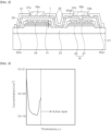
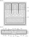
- FIG. 1 is a schematic plan view illustrating a light emitting diode according to an exemplary embodiment
- FIG. 2 is a cross-sectional view taken along the line A - A in FIG 1 .
- the light emitting diode includes a substrate 21, a first conductivity type semiconductor layer 23, an active layer 25, a second conductivity type semiconductor layer 27, a conductive oxide layer 28, a dielectric layer 29, a metal reflection layer 31, a lower insulation layer 33, a first pad metal layer 35a, a second pad metal layer 35b, and an upper insulation layer 37.
- the light emitting diode may further include a first bump pad 39a and a second bump pad 39b.
- the substrate 21 may be selected from any substrates that are suitable for growth of gallium nitride semiconductor layers thereon.
- the substrate 21 may include, for example, a sapphire substrate, a gallium nitride substrate, a SiC substrate, and the like, and may be a patterned sapphire substrate.
- the substrate 21 may have a rectangular or square shape, as shown in the plan view of FIG. 1 , without being limited thereto.
- a size of the substrate 21 is not particularly limited and may be selected in various ways.
- the first conductivity type semiconductor layer 23 is disposed on the substrate 21.
- the first conductivity type semiconductor layer 23 may be a gallium nitride semiconductor layer grown on the substrate 21 and doped with dopants, for example Si.
- An edge of the first conductivity type semiconductor layer 23 according to the exemplary embodiment is flush with an edge of the substrate 21.
- the inventive concepts are not limited thereto, and the first conductivity type semiconductor layer 23 may be located inside a region surrounded by the edge of the substrate 21. In this case, a portion of the upper surface of the substrate 21 may be exposed along a periphery of the first conductivity type semiconductor layer 23.
- a mesa M is disposed on the first conductivity type semiconductor layer 23.
- the mesa M may be disposed within a region surrounded by the first conductivity type semiconductor layer 23 so that regions near edges of the first conductivity type semiconductor layer 23 are not covered by the mesa M, but exposed to the outside.
- the mesa M includes the second conductivity type semiconductor layer 27 and the active layer 25.
- the active layer 25 is interposed between the first conductivity type semiconductor layer 23 and the second conductivity type semiconductor layer 27.
- the active layer 25 may have a single quantum well structure or a multiple quantum well structure.
- a location and a thickness of the well layer in the active layer 25 determine a wavelength of light that is generated. In particular, by controlling the location of the well layer, it is possible to provide an active layer generating ultraviolet light, blue light or green light.
- the second conductivity type semiconductor layer 27 may be a gallium nitride-based semiconductor layer doped with a p-type impurity, for example, Mg.
- a concentration of the p-type impurity of the second conductivity type semiconductor layer 27 affects a refractive index of the second conductivity type semiconductor layer 27.
- the concentration of the p-type impurity of the second conductivity type semiconductor layer 27 may be in a range of about 8 ⁇ 10 -18 to about 4 ⁇ 10 -21 /cm 3 . When the concentration of the impurity is lower than 8 ⁇ 10 -18 /cm 3 , effect that increases the refractive index is not obtained. When the concentration of the impurity is higher than 4 ⁇ 10 -21 /cm 3 , it is difficult to form a stable ohmic contact.
- a difference between the refractive index of the second conductivity type semiconductor layer 27 and that of the conductive oxide layer 28 may be increased by increasing the refractive index of the second conductivity type semiconductor layer 27.
- the difference in refractive indexes between the second conductivity type semiconductor layers 28 and the conductive oxide layer 28 is set to be substantially similar to the difference in refractive indexes between the conductive oxide layer 28 and the dielectric layer 29, and thus, light extraction may be effective.
- an edge of the lower insulation layer 33 may be formed to have a gentle inclination angle by forming the shape of the end terminal portion of the indent portion 30 and the shape of the end terminal portion of the first opening 33a2 of the lower insulation layer 33 as those in the illustrated exemplary embodiment, thereby improving yield of the light emitting diode.
- the dielectric layer 29 may cover the conductive oxide layer 28, and may further cover side surfaces of the second conductivity type semiconductor layer 27, the active layer 25, and the first conductivity type semiconductor layer 23.
- An edge of the dielectric layer 29 may be covered with the lower insulation layer 33. Accordingly, the edge of the dielectric layer 29 is located farther from the edge of the substrate 21 than the edge of the lower insulation layer 33.
- the inventive concepts are not limited thereto, and a portion of the dielectric layer 29 may be exposed to the outside of the lower insulation layer 33.
- the first opening 33a1 of the lower insulation layer 33 is formed to expose all of the peripheral region including the edge of the first conductivity type semiconductor layer 23 in the illustrated exemplary embodiment.
- the inventive concepts are not limited thereto, and the first opening 33a1 of the lower insulation layer 33 may be formed to have a band shape along the periphery of the mesa M.
- the edge of the first conductivity type semiconductor layer 23 may be covered with the lower insulation layer 33 or may be flush with the edge of the lower insulation layer 33.
- the outer contact portion 35a1 contacts the first conductivity type semiconductor layer 23 near the edge of the substrate 21 along the periphery of the mesa M, and the inner contact portion 35a2 contacts the first conductivity type semiconductor layer 23 in a region surrounded by the outer contact portion 35a1.
- the outer contact portion 35a1 and the inner contact portion 35a2 may be connected to each other, but the inventive concepts are not limited thereto, and they may be separated from each other.
- the outer contact portion 35a1 may continuously contact the first conductivity type semiconductor layer 23 along the periphery of the mesa M, but is not limited thereto, and a plurality of outer contact portions 35a1 may be disposed to be spaced apart from one another.
- the first pad metal layer 35a and the second pad metal layer 35b may be formed in the same process and may include substantially the same material.
- the first and second pad metal layers 35a and 35b may include an ohmic reflection layer such as an Al layer, and the ohmic reflection layer may be formed on an adhesive layer such as Ti, Cr, Ni, or the like.
- a protective layer of a single layer or a multiple layer structure such as Ni, Cr, Au, or the like may be formed on the ohmic reflection layer.
- the first and second pad metal layers 35a and 35b may have multilayer structures of Cr / Al / Ni / Ti / Ni / Ti / Au / Ti, for example.
- the upper insulation layer 37 may include a single layer of SiO 2 or Si 3 N 4 , without being limited thereto.
- the upper insulation layer 37 may have a multilayer structure which includes a silicon oxide layer and a silicon nitride layer, and may include a distributed Bragg reflector in which silicon oxide layers and titanium oxide layers are alternately stacked one above another.
- a reflective structure with the conductive oxide layer 28, the dielectric layer 29, and the metal reflection layer 31 is used instead of a conventional ohmic reflection layer.
- a bonding material such as solder from diffusing into the contact region, and to obtain a stable ohmic contact resistance, thereby improving the reliability of the light emitting diode.
- the thickness of the dielectric layer 29 is set to be about 300 nm or more, high light output and low forward voltage may be achieved.
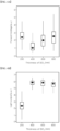
- a thickness of ITO was 20 nm, and thicknesses of SiO 2 were changed to 200 nm, 400 nm, 600 nm, and 800 nm.
- a thickness of the second conductivity type semiconductor layer 27 was about 65 nm.
- the lowest light output exhibited when the thickness of the dielectric layer 29 was 200 nm, and substantially similar light output exhibited when the thickness of the dielectric layer 29 was 400 nm or more.
- FIG. 5 is a schematic plan view illustrating a light emitting diode according to another exemplary embodiment
- FIG. 6 is a cross-sectional view taken along the line B-B of FIG. 5 .
- the light emitting diode according to the exemplary embodiment is substantially similar to the light emitting diode described with reference to FIGS. 1 and 2 , characteristic differences thereof will be mainly explained so as to avoid redundancy hereinafter.
- the edge of the first conductivity type semiconductor layer 23 is flush with the edge of the substrate 21, but an edge of a first conductivity type semiconductor layer 23 in the exemplary embodiment is disposed in a region surrounded by the edge of the substrate 21. As such, a region near the edge of the substrate 21 is exposed to the outside of the first conductivity type semiconductor layer 23.
- openings 29a of the dielectric layer 29 are adjusted in the exemplary embodiment, which will be described in detail later.
- the edge of the lower insulation layer 33 is located on the first conductivity type semiconductor layer 23, but, a lower insulation layer 33 in the exemplary embodiment covers the edge of the first conductivity type semiconductor layer 23, and is flush with the edge of the substrate 21.
- a first opening 33a1 of the lower insulation layer 33 is limitedly disposed on the first conductivity type semiconductor layer 23, and is disposed in a ring shape along a periphery of mesa M.
- a second opening 33b of the lower insulation layer 33 is formed at the outside of a second bump pad 39b so as not to overlap with the second bump pad 39b. Since the second opening 33b are disposed to be spaced apart from the second bump pad 39b in the lateral direction, it is possible to prevent solder from diffusing into the light emitting diode while soldering the second bump pad 39b.
- a first pad metal layer 35a covers the first opening 33a1 of the lower insulation layer 33 to contact the first conductivity type semiconductor layer 23, and thus, an outer contact portion 35a1 is formed in the first opening 33a1.
- the outer contact portion 35a1 may be connected to an inner contact portion 35a2 or spaced apart from the inner contact portion 35a2, as described in the previous exemplary embodiment.
- a shape of a second pad metal layer 35b in the exemplary embodiment is different from that of the second pad metal layer 35 in the exemplary embodiment of FIG. 1 , and accordingly, a location of a boundary region between the second pad metal layer 35b and the first pad metal layer 35a is also different from that in the exemplary embodiment of FIG. 1 .
- the second pad metal layer 35b extends to a region between the inner contact portion 35a2 and the outer contact portion 35a1.
- a front end of the second pad metal layer 35b may have a concave-convex shape as shown in the drawing.
- the first pad metal layer 35a may be spaced apart from the second pad metal layer 35b at regular intervals, and thus, the first pad metal layer 35a adjacent to the front end of the second pad metal layer 35b may also have a concave-convex shape.
- the front end of the second pad metal layer 35b extends to near the inner contact portions 35a2, it is possible to easily separate the second openings 33b of the lower insulation layer 33 from the second bump pad 39b in the lateral direction.
- An upper insulation layer 37 may cover the lower insulation layer 33, and an edge of the upper insulation layer 37 may be formed to be flush with the edges of the substrate 21 and the lower insulation layer 33.
- first and second bump pads 39a and 39b are illustrated and described as being disposed within the first and second openings 37a and 37b of the upper insulation layer 37 in the previous exemplary embodiment, first and second bump pads 39a and 39b cover and seal first and second openings 37a and 37b of the upper insulation layer 37 in the exemplary embodiment. That is, edges of the first and second bump pads 39a and 39b are located on an upper surface of the upper insulation layer 37. As such, the first pad metal layer 35a and the second pad metal layer 35b may be prevented from being exposed between the upper insulation layer 37 and the bump pads 39a and 39b, and thus, direct diffusion into the first and second pad metal layers 35a and 35b may be prevented.
- Locations of the edges of the first conductivity type semiconductor layer 23, the lower insulation layer 33, the upper insulation layer 37, and the bump pads 39a and 39b in the exemplary embodiment, are different from those in the exemplary embodiment of FIG. 1 , but the drawing herein is for illustrating an exemplary embodiment that can be modified with respect to the embodiment of FIG. 1 without being limited thereto. That is, the locations of the edges of the first conductivity type semiconductor layer 23, the lower insulation layer 33, and the upper insulation layer 37 in the exemplary embodiment may be the same as those of the embodiment of FIG. 1 , and the exemplary embodiment in FIG. 1 may be modified as that in the exemplary embodiment.
- the location of the openings 29a of a dielectric layer 29 in the exemplary embodiment are adjusted to enhance resistance to electrical overstress or electrostatic discharge.
- the reflective structure with the conductive oxide layer 28, the dielectric layer 29 and the metal reflection layer 31 improves the reflectance, the conductive oxide layer 28 and the metal reflection layer 31 need to be electrically connected.
- the openings 29a in the dielectric layer 29 provide a passage through which the metal reflection layer 31 electrically connects to the conductive oxide layer 28.
- a plurality of openings 29a are widely distributed on the conductive oxide layer 28 so as to evenly distribute current over a wide region of the conductive oxide layer 28.
- a distance between the outer contact portion 35a1 and the inner contact portion 35a2 and the openings 29a which are in contact with the first pad metal layer 35a may affect characteristics of the light emitting diode against electrical overstress or electrostatic discharge.
- the illustrated exemplary embodiment as shown in FIG. 5 is characterized in that, among the openings 29a of the dielectric layer 29 disposed under the first opening 37a of the upper insulation layer 37 (or under the first bump pad 39a), the openings 29a located closest to the inner contact portion 35a2 are relatively spaced apart therefrom.
- a shortest distance Dv1 between the outer contact portion 35a1 and the opening 29a located under the first opening 37a of the upper insulation layer 37 is greater than a shortest distance Ds between the outer contact portion 35a1 and the openings 29a located outside the first openings 37a of the upper insulation layer 37.
- the distance between the opening 29a of the dielectric layer 29 located under the first bump pad 39a electrically connected to the first conductivity type semiconductor layer 23 and the contact portions 35a1 and 35a2 is greatly affected by electrical overstress and electrostatic discharge. Accordingly, the reliability of the light emitting diode may be improved by separating the openings 29a of the dielectric layer 29 located under the first bump pad 39a far away from the contact portions 35a1 and 35a2.
- the openings 29a under the second bump pad 39b and those in other locations as well as the openings 29a under the first bump pad 39a may also be separated from the contact portions 35a1 and 35a2, but luminous efficiency may be lowered because current may not be widely distributed in this case. Therefore, the electrostatic discharge characteristics may be improved in the illustrated exemplary embodiment by arranging only the openings 29a located under the first bump pad 39a relatively far from other openings without deteriorating the current spreading performance.
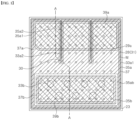
- FIG. 7 is a schematic plan view illustrating a light emitting diode according to another exemplary embodiment.
- the light emitting diode according to the exemplary embodiment is substantially similar to the light emitting diode described with reference to FIGS. 5 and 6 , but openings of a dielectric layer 29 include elongated opening 29b along with a plurality of openings 29a in the exemplary embodiment.
- the opening 29b When the opening 29b is located between an outer contact portion 35a1 and an inner contact portion 35a2 and the openings 29a, the opening 29b forms a closed loop along the outer contact portion 35a1 and the inner contact portion 35a2. Since the openings 29b adjacent to the outer contact portion 35a1 and the inner contact portion 35a2 are lengthily adjacent to the contact portions 35a1 and 35a2, it is possible to prevent a large difference in voltage from occurring at a specific point, and thus a light emitting diode having a strong resistance to electrical overstress or electrostatic discharge may be provided.
- the opening 29b in the illustrated exemplary embodiment is shown and described as forming the closed loop, the openings 29b that has a shape having a length larger than a width may be arranged along the contact portions 35a1 and 35a2.
- the opening 29b is not limitedly disposed under a first bump pad 39a but also extends to the outside of the first bump pad 39a, but the opening 29b may be limitedly disposed under the first bump pad 39a.
- FIG. 8 is a schematic plan view illustrating a light emitting diode according to another exemplary embodiment.
- the light emitting diode according to the exemplary embodiment is substantially similar to the light emitting diode described with reference to FIG. 7 , but openings of a dielectric layer 29 further include an opening 29c in the exemplary embodiment.
- the opening 29c may be disposed in a region surrounded by opening 29b, and in particular, may be located outside of a lower region of a second bump pad 39b. A portion of the opening 29c may also be located under the first bump pad 39b.
- the light emitting diode according to the exemplary embodiment is substantially similar to the light emitting diode described with reference to FIG. 5 , but a mesa M has an elongated shape in one direction, outer contact portions 35a1 are formed near an edge of the mesa without inner contact portions 35a2, and a first pad metal layer 35a is formed not to surround a second pad metal layer 35b.
- the mesa M has an elongated shape in one direction, and for example, a length thereof may be more than four times longer and less than seven times longer than a width thereof.
- the mesa M is formed to have an elongated shape in one direction, and thus, a region where the first pad metal layer 35a contacts a first conductivity type semiconductor layer 23 may be relatively reduced, thereby ensuring the light emitting area.
- a dielectric layer 29 covers a conductive oxide layer 28 and covers a side surface of the mesa M. A portion of the dielectric layer 29 partially covers the first conductivity type semiconductor layer 23 exposed around the mesa M as described with reference to FIG. 5 .
- the dielectric layer 29 has a plurality of openings 29a exposing the conductive oxide layer 28, and locations of the openings 29a are adjusted to improve resistance to electrical overstress and electrostatic discharge. This will be described later.
- the conductive oxide layer 28 and the metal reflection layer 31 cover most of an upper surface of the mesa M.
- edges of the conductive oxide layer 28 and the metal reflection layer 31 are spaced apart from the edge of the mesa M, and in particular, spaced farther from one edge of the mesa M that is adjacent to the outer contact portions 35a1.
- the edge of the conductive oxide layer 28 is spaced farther from the outer contact portions 35, it is possible to prevent the occurrence of device failure due to electrical overstress or electrostatic discharge.
- a lower insulation layer 33 may cover the dielectric layer 29 and the metal reflection layer 31, and may cover a portion of the first conductivity type semiconductor layer 23 exposed around the mesa M.
- the lower insulation layer 33 exposes the first conductivity type semiconductor layer 23 in recess regions of the mesa M.
- the lower insulation layer 33 may cover the first conductivity type semiconductor layer 23, it may be formed to expose a region near an edge of the first conductivity type semiconductor layer 23 as shown in the drawing.
- the lower insulation layer 33 also has a second opening 33b exposing the metal reflection layer 31.
- the first pad metal layer 35a in the illustrated exemplary embodiment is disposed over the mesa M except for a region where the outer contact portions 35a1 are formed.
- the first pad metal layer 35a covers not only the upper region of the mesa M but also the side surface of the mesa M and a portion of the first conductivity type semiconductor layer 23 around the mesa M.
- An edge of the first pad metal layer 35a may also be located on the mesa M in a region between the recesses of the mesa M.
- the second pad metal layer 35b may be disposed in the upper region of the mesa M.
- the second pad metal layer 35b may be formed lengthily along the region having the narrow width of the first pad metal layer 35a.
- the second pad metal layer 35b may be electrically connected to the metal reflection layer 31 through the second openings 33b of the lower insulation layer 33.
- the second openings 33b of the lower insulation layer 33 may be disposed under the second bump pad 39b, but may be spaced apart from the second bump pad 39b in the lateral direction as illustrated in the drawing.
- the openings 29a of the dielectric layer 29 are disposed apart from the edges of the mesas M, and in particular, disposed farther apart from the edge of the mesas M adjacent to the outer contact portions 35a1.
- a distance Dv1 of the opening 29a that is most closely disposed apart from the outer contact portion 35a1 in the vertical direction is greater than a distance Ds of the opening 29a that is disposed closest to the contact portion 35a1.
- the opening 29a that is disposed closest to the contact portion 35a1 is disposed farther from the edge of the mesa M than the opening closest to the edge of the mesa M.
- FIG. 10 is a schematic plan view illustrating a light emitting diode according to another exemplary embodiment.
- the light emitting diode according to the exemplary embodiment is substantially similar to the light emitting diode described with reference to FIG. 9 , but a dielectric layer 29 has openings 29a and 129a that have different sizes from each other in the exemplary embodiment.
- relatively large openings 129a are disposed closer to outer contact portions 35a1 than relatively small openings 29a.
- the relatively large openings 129a in a lower region of a first bump pad 39a are disposed closer to the outer contact portion 35a1 than the relatively small openings 29a.
- the relatively large openings 129a may also be disposed closer to the outer contact portions 35a1 than the relatively small openings 29a in a lower region of the second bump pad 39b and other regions.
- the relatively large openings 129a may prevent current from being concentrated at a specific point, thereby improving resistance of the light emitting diode to electrical overstress or electrostatic discharge.
- the openings 129a in the illustrated exemplary embodiment are shown as being circular, but their shapes may vary.
- the openings 129a may have an elongated shape along the longitudinal direction of the mesa M, and for example, may have an ellipse shape or a bar shape.
- FIG. 11 is a schematic plan view illustrating a light emitting diode according to another exemplary embodiment.
- the opening 129b is disposed between the outer contact portion 35a1 and openings 29a to prevent current from being concentrated at a specific point, thereby improving the light emitting diode's resistance to electrical overstress or electrostatic discharge. End portions of the bar-shaped openings 129b may be formed to have a relatively wide width to facilitate patterning.
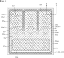
- FIG. 12 is a schematic plan view illustrating a light emitting diode according to another exemplary embodiment.
- the light emitting diode according to the exemplary embodiment is substantially similar to the light emitting diode described with reference to FIG. 11 , but a single bar-shaped opening 129c is formed continuously over outer contact portions 35a1.
- the bar-shaped opening 129c is not necessarily a straight line.
- a portion of the opening 129c disposed under a first bump pad 39a may be disposed farther from the outer contact portion 35a1 than other portions.
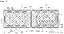
- FIG. 13 is a schematic plan view illustrating a light emitting diode according to another exemplary embodiment of the present disclosure
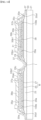
- FIG. 14 is a cross-sectional view taken along the line C-C of FIG. 13 .
- the isolation region I separates the light emitting cells C1 and C2 from each other. As such, a surface of the substrate 21 is exposed in the isolation region I through semiconductor layers.
- the isolation region I is formed using photolithography and etching processes, a photoresist pattern having a gentle inclined surface is formed and the semiconductor layers are etched using the photoresist pattern as a mask, thereby forming relatively gently inclined side surfaces in the isolation region I.
- the light emitting cells C1 and C2 face each other with the isolation region I interposed therebetween.
- Side surfaces of the light emitting cells C1 and C2 that face each other are defined as inner side surfaces, and side surfaces of the light emitting cells other than the inner side surfaces are defined as outer side surfaces. Therefore, the first conductivity type semiconductor layers 23 in the first and second light emitting cells C1 and C2 also include inner and outer side surfaces, respectively.
- the first conductivity type semiconductor layer 23 may include one inner side surface and three outer side surfaces.
- Each mesa M includes a second conductivity type semiconductor layer 27 and an active layer 25.
- the active layer 25 is interposed between the first conductivity type semiconductor layer 23 and the second conductivity type semiconductor layer 27.
- Each mesa M has recesses, first openings 33a of a lower insulation layer 33 are formed in the recesses, which will be described later, and outer contact portions 35a1 are formed through the first openings 33a.
- a conductive oxide layer 28 is disposed on each mesa M, and a dielectric layer 29 covers the conductive oxide layer 28 and the mesa M on each of the light emitting cells C1 and C2.
- the conductive oxide layer 28 is in ohmic contact with the second conductivity type semiconductor layer 27.
- the conductive oxide layer 28 may be disposed over almost an entire region of the mesa M in an upper region of the mesa M. However, the conductive oxide layer 28 may be spaced apart from an edge of the mesa M.
- a metal reflection layer 31 is disposed on the dielectric layer 29 and connects to the conductive oxide layer 28 through the openings 29a and 129b of the dielectric layer 29.
- the metal reflection layer 31 is disposed in the upper region of the mesa M of each of the light emitting cells C1 and C2.
- the lower insulation layer 33 includes the first openings 33a exposing the first conductivity type semiconductor layer 23 in the recesses of each mesa M, and further includes second openings 33b 1 exposing the metal reflection layer 31 on the second light emitting cell C2 and a third opening 33b2 exposing the metal reflection layer 31 on the first light emitting cell C1.
- the first openings 33a expose the first conductivity type semiconductor layer 23 along outer surfaces of the mesa M
- the third opening 33b2 exposes the metal reflection layer 31 on the first light emitting cell C1 near the isolation region I.
- the third openings 33b2 may generally have an elongated shape along the isolation region I, but are not necessarily limited thereto, and may have various shapes.
- the second openings 33b1 may be located on the second light emitting cell C2, and may be located in a lower region of a second bump pad 39b. However, in another exemplary embodiment, the second openings 33b1 may be disposed to be apart from the second bump pad 39b on the second light emitting cell C2 in the lateral direction.
- the first pad metal layer 35a is disposed on the first light emitting cell C, and is in ohmic contact with the first conductivity type semiconductor layer 23 exposed around the mesa M. As shown in FIG. 13 , the first pad metal layer 35a may be in ohmic contact with the first conductivity type semiconductor layer 23 through the first opening 33a of the lower insulation layer 33 along a periphery of the mesa M to form the outer contact portions 35a1. In the drawing, the first pad metal layer 35a intermittently contacts the first conductivity type semiconductor layer 23 in the recesses of the mesa M along the periphery of the mesa M, but is not limited thereto, and may continuously contact the first conductivity type semiconductor layer 23.
- the bar-shaped openings 129b of the dielectric layer 29 may be flush with the first openings 33a of the lower insulation layer 33, and thus, may be flush with the outer contact portions 35a1.
- the second pad metal layer 35b is disposed on the second light emitting cell C2 and is connected to the metal reflection layer 31 on the second light emitting cell C2 through the second opening 33b1 of the lower insulation layer 33.
- the second pad metal layer 35b is disposed on the mesa M, and is insulated from the first conductivity type semiconductor layer 23.
- the second pad metal layer 35b may be separated from side surfaces of the mesa M on the second light emitting cell C2.
- connection metal layer 35c may be electrically connected to the metal reflection layer 31 on the first light emitting cell C1 through the third opening 33b2 of the lower insulation layer 33, and may be electrically connected to the first conductivity type semiconductor layer 23 of the second light emitting cell C2 through the first openings 33a of the second light emitting cell C2. Accordingly, the first and second light emitting cells C1 and C2 are connected to each other in series through the connection metal layer 33c.
- the first and second pad metal layers 35a and 35b and the connection metal layer 35c may be formed in the same process and may include substantially the same material.
- the first and second pad metal layers 35a and 35b and the connection metal layer 35c may include an ohmic reflection layer such as an Al layer, and the ohmic reflection layer may be formed on an adhesive layer such as Ti, Cr, or Ni.
- a protective layer of a single layer or a multiple layer structure such as Ni, Cr, Au, or the like may be formed on the ohmic reflection layer.
- the first and second pad metal layers 35a and 35b and the connection metal layer 35c may have multilayer structures of Cr/Al/Ni/Ti/Ni/Ti/Au/Ti, for example.
- the upper insulation layer 37 is disposed on the first pad metal layer 35a, the second pad metal layer 35b, and the connection metal layer 35c, and has a first opening 37a exposing the first pad metal layer 35a and a second opening 37b exposing the second pad metal layer 35b.
- the upper insulation layer 37 also covers the first pad metal layer 35a and the connection metal layer 35c connected to the first conductivity type semiconductor layer 23 in the periphery of the mesa M. As shown in FIG. 13 , a region between the first pad metal layer and the second connection metal layer 35c and an edge of the first conductivity type semiconductor layer 23 is covered with the upper insulation layer 37.
- the upper insulation layer 37 may cover the connection metal layer 35c on the isolation region I, and may be formed to have irregularities according to a shape of the connection metal layer 35c.
- the upper insulation layer 37 protects the first and second pad metal layers 35a and 35b and the connection metal layer 35c from external environments such as moisture.
- the first opening 37a is formed within an upper region of the first pad metal layer 35a, and thus is separated from the connection metal layer 35c and the third opening 33b2 of the lower insulation layer 33.
- the second opening 37b is also disposed limitedly on the second pad metal layer 35b, and is separated from the connection metal layer 35c.
- the first and second pad metal layers 35a and 35b exposed through the first and second openings 37a and 37b of the upper insulation layer 37 may serve as bonding pads to which the solder is directly bonded.
- the first and second bump pads 39a and 39b may cover the first and second pad metal layers 35a and 35b exposed through the first and second openings 37a and 37b of the upper insulation layer 37, respectively.
- the first and second bump pads 39a and 39b may be formed in the first and second openings 37a and 37b of the upper insulation layer 37, but the inventive concepts are not limited thereto, and the first and second bump pads 39a and 39b may cover and seal the first and second openings 37a and 37b.
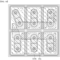
- FIG. 15 is a schematic plan view illustrating a light emitting diode according to another exemplary embodiment.
- the light emitting diode includes six light emitting cells C1, C2, C3, C4, C5, and C6, and the light emitting cells are connected in series.
- Each of the light emitting cells C1 C2, C3, C4, C5, and C6 includes a first conductivity type semiconductor layer 23 and a mesa M as described with reference to FIG. 13 , and is separated from one another by an isolation region.
- Each mesa M has a via hole 30a exposing the first conductivity type semiconductor layer 23, and a lower insulation layer 33 has a first opening 33a exposing the first conductivity type semiconductor layer 23 in each via hole 30a.
- the lower insulation layer 33 has a second opening 33b exposing a metal reflection layer 31 on each light emitting cell.
- a first pad metal layer 35a is disposed on the first light emitting cell C1 and forms inner contact portions 35a2 in the via holes 30a in the first light emitting cell C1.
- a second pad metal layer 35b is disposed on the last light emitting cell, that is, the sixth light emitting cell C6, and is connected to the metal reflection layer 31 through the second opening 33b.
- Connection metal layers 35c connect adjacent light emitting cells in series.
- the connection metal layers 35c electrically connect the metal reflection layer 31 of the adjacent light emitting cells and the first conductivity type semiconductor layer 23.
- the inner contact portions 35a2 are formed in the via holes 30a of the second, third, fourth, fifth, and sixth light emitting cells C2, C2, C3, C4, C5, and C6 by the connection metal layers 35c.
- a first bump pad 39a is disposed on the first light emitting cell C1 and a second bump pad 39b is disposed on the sixth light emitting cell C6.
- the first, second, third, fourth, fifth, and sixth light emitting cells C1, C2, C2, C3, C4, C5, and C6 are connected in series between the first bump pad 39a and the second bump pad 39b.
- FIG. 17 is an exploded perspective view illustrating a lighting apparatus to which a light emitting diode according to an exemplary embodiment is applied.
- the lighting apparatus includes a diffusive cover 1010, a light emitting diode module 1020, and a body 1030.
- the body 1030 may receive the light emitting diode module 1020 and the diffusive cover 1010 may be disposed on the body 1030 to cover an upper surface of the light emitting diode module 1020.
- FIG. 18 is a cross-sectional view illustrating a display apparatus to which a light emitting diode according to another exemplary embodiment of the present disclosure is applied.
- the display panel 2110 is not particularly limited and may be, for example, a liquid crystal panel including a liquid crystal layer.
- Gate driving PCBs may be further disposed at the periphery of the display panel 2110 to supply driving signals to a gate line.
- the gate driving PCBs may be formed on a thin film transistor substrate instead of being formed on separate PCBs.
- the bottom cover 2180 may be open at an upper surface thereof to receive the substrate, the light emitting diodes 2160, the reflective sheet 2170, the diffusive plate 2131, and the optical sheets 2130.
- the bottom cover 2180 may be coupled to the panel guide.
- the substrate may be disposed under the reflective sheet 2170 to be surrounded by the reflective sheet 2170.
- the substrate may be disposed on the reflective sheet 2170.
- a plurality of substrates may be arranged flush with one another, without being limited thereto.
- the backlight unit includes a single substrate.
- the light emitting diodes 2160 may include at least one of the light emitting diodes according to the exemplary embodiments described above.
- the light emitting diodes 2160 may be regularly arranged in a predetermined pattern on the substrate.
- a lens 2210 may be disposed on each of the light emitting diodes 2160 to improve uniformity of light emitted from the plurality of light emitting diodes 2160.
- the light emitting diodes according to the exemplary embodiments may be applied to direct type displays like the display apparatus according to the exemplary embodiment.
- FIG. 19 is a cross-sectional view illustrating a display apparatus to which a light emitting diode according to another exemplary embodiment of the present disclosure is applied.
- the display apparatus includes a display panel 3210 on which an image is displayed, and a backlight unit disposed at a rear side of the display panel 3210 and emitting light thereto. Further, the display apparatus includes a frame 240 supporting the display panel 3210 and receiving the backlight unit, and covers 3240, 3280 surrounding the display panel 3210.
- the display panel 3210 is not particularly limited and may be, for example, a liquid crystal panel including a liquid crystal layer.
- a gate driving PCB may be further disposed at the periphery of the display panel 3210 to supply driving signals to a gate line.
- the gate driving PCB may be formed on a thin film transistor substrate instead of being formed on a separate PCB.
- the display panel 3210 is secured by the covers 3240, 3280 disposed at upper and lower sides thereof, and the cover 3280 disposed at the lower side of the display panel 3210 may be coupled to the backlight unit.
- the backlight unit supplying light to the display panel 3210 includes a lower cover 3270 partially open at an upper surface thereof, a light source module disposed at one side inside the lower cover 3270, and a light guide plate 3250 disposed flush with the light source module and converting spot light into sheet light.
- the backlight unit according to the exemplary embodiment may further include optical sheets 3230 disposed on the light guide plate 3250 to spread and collect light, and a reflective sheet 3260 disposed at a lower side of the light guide plate 3250 and reflecting light traveling in a downward direction of the light guide plate 3250 towards the display panel 3210.
- the light source module includes a substrate 3220 and a plurality of light emitting diodes 3110 arranged at constant intervals on one surface of the substrate 3220.
- the substrate 3220 any substrate capable of supporting the light emitting diodes 3110 and being electrically connected thereto may be used without limitation.
- the substrate 3220 may include a printed circuit board.
- the light emitting diodes 3110 may include at least one of the light emitting diodes according to the exemplary embodiments described above.
- Light emitted from the light source module enters the light guide plate 3250 and is supplied to the display panel 3210 through the optical sheets 3230.
- the light guide plate 3250 and the optical sheets 3230 convert spot light emitted from the light emitting diodes 3110 into sheet light.
- the light emitting diodes according to the exemplary embodiments may be applied to edge type displays like the display apparatus according to the exemplary embodiment.
- FIG. 20 is a cross-sectional view illustrating a head light to which a light emitting diode according to another exemplary embodiment of the present disclosure is applied.
- the headlight includes a lamp body 4070, a substrate 4020, a light emitting diode 4010, and a cover lens 4050.
- the headlight may further include a heat dissipation unit 4030, a support rack 4060, and a connection member 4040.
- the substrate 4020 is secured by the support rack 4060 and is disposed above the lamp body 4070.
- the substrate 4020 any member capable of supporting the light emitting diode 4010 may be used without limitation.
- the substrate 4020 may include a substrate having a conductive pattern, such as a printed circuit board.
- the light emitting diode 4010 is disposed on the substrate 4020 and may be supported and secured by the substrate 4020.
- the light emitting diode 4010 may be electrically connected to an external power source through the conductive pattern of the substrate 4020.
- the light emitting diode 4010 may include at least one of the light emitting diodes according to the exemplary embodiments described above.
- the cover lens 4050 is disposed on a path of light emitted from the light emitting diode 4010.
- the cover lens 4050 may be separated from the light emitting diode 4010 by the connection member 4040 and may be disposed in a direction of supplying light emitted from the light emitting diode 4010.
- the connection member 4040 is disposed to secure the cover lens 4050 to the substrate 4020 while surrounding the light emitting diode 4010, and thus can act as a light guide that provides a luminous path 4045.
- the connection member 4040 may include a light reflective material or coated therewith.
- the heat dissipation unit 4030 may include heat dissipation fins 4031 and/or a heat dissipation fan 4033 to dissipate heat generated upon operation of the light emitting diode 4010.
- the light emitting diodes according to the exemplary embodiments may be applied to headlights like the headlight according to the exemplary embodiment, particularly, vehicular headlights.
Landscapes
- Led Devices (AREA)
Applications Claiming Priority (4)
| Application Number | Priority Date | Filing Date | Title |
|---|---|---|---|
| KR1020170178222A KR102440223B1 (ko) | 2017-12-22 | 2017-12-22 | 칩 스케일 패키지 발광 다이오드 |
| KR1020180156201A KR102601421B1 (ko) | 2018-12-06 | 2018-12-06 | 칩 스케일 패키지 발광 다이오드 |
| EP18890348.8A EP3716346B1 (fr) | 2017-12-22 | 2018-12-10 | Diode électroluminescente à boîtier à l'échelle d'une puce |
| PCT/KR2018/015628 WO2019124843A1 (fr) | 2017-12-22 | 2018-12-10 | Diode électroluminescente à boîtier à l'échelle d'une puce |
Related Parent Applications (1)
| Application Number | Title | Priority Date | Filing Date |
|---|---|---|---|
| EP18890348.8A Division EP3716346B1 (fr) | 2017-12-22 | 2018-12-10 | Diode électroluminescente à boîtier à l'échelle d'une puce |
Publications (2)
| Publication Number | Publication Date |
|---|---|
| EP4297105A2 true EP4297105A2 (fr) | 2023-12-27 |
| EP4297105A3 EP4297105A3 (fr) | 2024-04-24 |
Family
ID=66994071
Family Applications (2)
| Application Number | Title | Priority Date | Filing Date |
|---|---|---|---|
| EP18890348.8A Active EP3716346B1 (fr) | 2017-12-22 | 2018-12-10 | Diode électroluminescente à boîtier à l'échelle d'une puce |
| EP23208095.2A Pending EP4297105A3 (fr) | 2017-12-22 | 2018-12-10 | Diode électroluminescente à boîtier à puce |
Family Applications Before (1)
| Application Number | Title | Priority Date | Filing Date |
|---|---|---|---|
| EP18890348.8A Active EP3716346B1 (fr) | 2017-12-22 | 2018-12-10 | Diode électroluminescente à boîtier à l'échelle d'une puce |
Country Status (4)
| Country | Link |
|---|---|
| US (5) | US10998469B2 (fr) |
| EP (2) | EP3716346B1 (fr) |
| CN (4) | CN115621387A (fr) |
| WO (1) | WO2019124843A1 (fr) |
Families Citing this family (20)
| Publication number | Priority date | Publication date | Assignee | Title |
|---|---|---|---|---|
| US20190189850A1 (en) * | 2017-12-19 | 2019-06-20 | Epistar Corporation | Light-emitting device |
| CN115621387A (zh) | 2017-12-22 | 2023-01-17 | 首尔伟傲世有限公司 | 发光二极管 |
| DE102019113119A1 (de) * | 2019-05-17 | 2020-11-19 | OSRAM Opto Semiconductors Gesellschaft mit beschränkter Haftung | Optoelektronischer Halbleiterchip und Verfahren zur Herstellung eines optoelektronischen Halbleiterchips |
| CN110459660B (zh) * | 2019-08-06 | 2021-04-16 | 天津三安光电有限公司 | 一种发光二极管及制作工艺、发光装置 |
| CN113363366B (zh) * | 2020-03-06 | 2024-04-19 | 隆达电子股份有限公司 | 发光元件 |
| US11387334B2 (en) * | 2020-04-24 | 2022-07-12 | Renesas Electronics Corporation | Semiconductor device with electrode plating deposition |
| WO2022015103A1 (fr) * | 2020-07-17 | 2022-01-20 | 서울바이오시스주식회사 | Diode électroluminescence ultraviolette profonde |
| CN112201735B (zh) * | 2020-09-03 | 2022-08-19 | 厦门三安光电有限公司 | 半导体发光二极管及其制备方法 |
| US12272765B2 (en) * | 2020-09-24 | 2025-04-08 | Seoul Viosys Co., Ltd. | High efficiency light emitting device, unit pixel having the same, and displaying apparatus having the same |
| US12310152B2 (en) | 2021-05-20 | 2025-05-20 | Nichia Corporation | Light emitting element including substrate, emission parts, insulation layer, and electrodes |
| KR20230013705A (ko) * | 2021-07-19 | 2023-01-27 | 삼성디스플레이 주식회사 | 발광 소자 및 이를 포함하는 표시 장치 |
| CN113644180B (zh) * | 2021-08-05 | 2023-01-06 | 厦门士兰明镓化合物半导体有限公司 | 倒装led芯片及其制备方法 |
| US12557460B2 (en) * | 2021-09-14 | 2026-02-17 | Xiamen San'an Optoelectronics Co., Ltd | Light-emitting diode and light-emitting module having the same |
| CN113782658B (zh) * | 2021-11-10 | 2022-02-11 | 华引芯(武汉)科技有限公司 | 发光半导体及其制备方法 |
| TW202329483A (zh) * | 2022-01-05 | 2023-07-16 | 晶元光電股份有限公司 | 發光元件 |
| US20240072099A1 (en) * | 2022-08-25 | 2024-02-29 | Creeled, Inc. | Light-emitting diode chip structures |
| TWI827271B (zh) * | 2022-09-23 | 2023-12-21 | 國立清華大學 | 光電元件 |
| CN116031345A (zh) * | 2022-12-23 | 2023-04-28 | 厦门三安光电有限公司 | 一种发光二极管 |
| US20250267986A1 (en) * | 2024-02-19 | 2025-08-21 | Seoul Viosys Co., Ltd. | Light emitting device and light emitting apparatus including the same |
| CN121078859A (zh) * | 2025-11-07 | 2025-12-05 | 江西兆驰半导体有限公司 | 倒装led芯片及其制备方法 |
Family Cites Families (22)
| Publication number | Priority date | Publication date | Assignee | Title |
|---|---|---|---|---|
| JP4507358B2 (ja) * | 2000-06-16 | 2010-07-21 | 日亜化学工業株式会社 | 光半導体素子 |
| DE102007019776A1 (de) * | 2007-04-26 | 2008-10-30 | Osram Opto Semiconductors Gmbh | Optoelektronisches Bauelement und Verfahren zur Herstellung einer Mehrzahl optoelektronischer Bauelemente |
| JP2009164423A (ja) * | 2008-01-08 | 2009-07-23 | Nichia Corp | 発光素子 |
| JP5633477B2 (ja) * | 2010-08-27 | 2014-12-03 | 豊田合成株式会社 | 発光素子 |
| JP5949294B2 (ja) * | 2011-08-31 | 2016-07-06 | 日亜化学工業株式会社 | 半導体発光素子 |
| KR101691589B1 (ko) * | 2011-09-16 | 2017-01-02 | 서울바이오시스 주식회사 | 발광 다이오드 및 그것을 제조하는 방법 |
| CN106058000B (zh) * | 2011-09-16 | 2019-04-23 | 首尔伟傲世有限公司 | 发光二极管及制造该发光二极管的方法 |
| JP5768759B2 (ja) * | 2012-04-27 | 2015-08-26 | 豊田合成株式会社 | 半導体発光素子 |
| DE112013005849T5 (de) * | 2012-12-06 | 2015-08-20 | Seoul Viosys Co., Ltd. | Lichtemittierende Diode und Anwendung dafür |
| KR101546929B1 (ko) * | 2013-09-24 | 2015-08-25 | 서울바이오시스 주식회사 | 발광 다이오드 및 그것을 갖는 발광 다이오드 모듈 |
| US9577171B2 (en) * | 2014-06-03 | 2017-02-21 | Seoul Viosys Co., Ltd. | Light emitting device package having improved heat dissipation efficiency |
| WO2015190817A1 (fr) * | 2014-06-10 | 2015-12-17 | 주식회사 세미콘라이트 | Élément électroluminescent à semi-conducteur |
| KR20160016361A (ko) * | 2014-08-05 | 2016-02-15 | 서울바이오시스 주식회사 | 발광 다이오드 및 그 제조 방법 |
| KR20160037060A (ko) * | 2014-09-26 | 2016-04-05 | 서울바이오시스 주식회사 | 발광소자 및 그 제조 방법 |
| KR102323686B1 (ko) * | 2014-10-21 | 2021-11-11 | 서울바이오시스 주식회사 | 발광 소자 및 그 제조 방법 |
| JP2016143682A (ja) * | 2015-01-29 | 2016-08-08 | 豊田合成株式会社 | Iii族窒化物半導体発光素子 |
| KR102303460B1 (ko) * | 2015-03-31 | 2021-09-17 | 쑤저우 레킨 세미컨덕터 컴퍼니 리미티드 | 발광 소자 및 이를 포함하는 발광 소자 패키지 |
| KR20170009359A (ko) * | 2015-07-16 | 2017-01-25 | 서울바이오시스 주식회사 | 발광 소자 및 그것을 제조하는 방법 |
| KR102471670B1 (ko) * | 2016-02-11 | 2022-11-29 | 서울바이오시스 주식회사 | 고출력 발광 다이오드 및 그것을 갖는 발광 모듈 |
| KR101826949B1 (ko) * | 2017-04-06 | 2018-02-07 | 서울바이오시스 주식회사 | 발광 다이오드 |
| KR101843512B1 (ko) * | 2017-05-22 | 2018-05-14 | 서울바이오시스 주식회사 | 표면 실장용 발광 다이오드 모듈 및 이의 제조방법. |
| CN115621387A (zh) | 2017-12-22 | 2023-01-17 | 首尔伟傲世有限公司 | 发光二极管 |
-
2018
- 2018-12-10 CN CN202211241597.XA patent/CN115621387A/zh not_active Withdrawn
- 2018-12-10 CN CN201911394635.3A patent/CN111129265B/zh active Active
- 2018-12-10 CN CN202211241646.XA patent/CN115621388A/zh not_active Withdrawn
- 2018-12-10 EP EP18890348.8A patent/EP3716346B1/fr active Active
- 2018-12-10 CN CN201880005632.3A patent/CN110192287B/zh active Active
- 2018-12-10 WO PCT/KR2018/015628 patent/WO2019124843A1/fr not_active Ceased
- 2018-12-10 EP EP23208095.2A patent/EP4297105A3/fr active Pending
-
2020
- 2020-05-28 US US16/885,536 patent/US10998469B2/en active Active
-
2021
- 2021-01-25 US US17/157,600 patent/US11557696B2/en active Active
-
2023
- 2023-01-11 US US18/153,205 patent/US11862455B2/en active Active
- 2023-08-14 US US18/449,179 patent/US12349517B2/en active Active
-
2025
- 2025-06-24 US US19/247,589 patent/US20250324825A1/en active Pending
Also Published As
| Publication number | Publication date |
|---|---|
| US20200295229A1 (en) | 2020-09-17 |
| US11557696B2 (en) | 2023-01-17 |
| CN115621388A (zh) | 2023-01-17 |
| CN110192287A (zh) | 2019-08-30 |
| CN111129265A (zh) | 2020-05-08 |
| CN111129265B (zh) | 2023-06-02 |
| US20240055563A1 (en) | 2024-02-15 |
| EP3716346C0 (fr) | 2023-11-08 |
| CN115621387A (zh) | 2023-01-17 |
| EP3716346A1 (fr) | 2020-09-30 |
| US20230299240A1 (en) | 2023-09-21 |
| EP3716346B1 (fr) | 2023-11-08 |
| US10998469B2 (en) | 2021-05-04 |
| US12349517B2 (en) | 2025-07-01 |
| CN110192287B (zh) | 2022-10-28 |
| US11862455B2 (en) | 2024-01-02 |
| US20250324825A1 (en) | 2025-10-16 |
| EP3716346A4 (fr) | 2021-08-25 |
| EP4297105A3 (fr) | 2024-04-24 |
| US20210151628A1 (en) | 2021-05-20 |
| WO2019124843A1 (fr) | 2019-06-27 |
Similar Documents
| Publication | Publication Date | Title |
|---|---|---|
| US12349517B2 (en) | Chip-scale package light emitting diode | |
| US12302679B2 (en) | Light emitting diode | |
| US10998479B2 (en) | Light emitting diode | |
| US11183620B2 (en) | Light emitting diode having a plurality of light emitting cells | |
| US11749707B2 (en) | Chip-scale package light emitting diode | |
| KR102601421B1 (ko) | 칩 스케일 패키지 발광 다이오드 | |
| KR20200112410A (ko) | 발광 다이오드 | |
| KR102562475B1 (ko) | 칩 스케일 패키지 발광 다이오드 |
Legal Events
| Date | Code | Title | Description |
|---|---|---|---|
| PUAI | Public reference made under article 153(3) epc to a published international application that has entered the european phase |
Free format text: ORIGINAL CODE: 0009012 |
|
| STAA | Information on the status of an ep patent application or granted ep patent |
Free format text: STATUS: THE APPLICATION HAS BEEN PUBLISHED |
|
| AC | Divisional application: reference to earlier application |
Ref document number: 3716346 Country of ref document: EP Kind code of ref document: P |
|
| AK | Designated contracting states |
Kind code of ref document: A2 Designated state(s): AL AT BE BG CH CY CZ DE DK EE ES FI FR GB GR HR HU IE IS IT LI LT LU LV MC MK MT NL NO PL PT RO RS SE SI SK SM TR |
|
| REG | Reference to a national code |
Ref country code: DE Ref legal event code: R079 Free format text: PREVIOUS MAIN CLASS: H01L0033400000 Ipc: H01L0033480000 |
|
| PUAL | Search report despatched |
Free format text: ORIGINAL CODE: 0009013 |
|
| AK | Designated contracting states |
Kind code of ref document: A3 Designated state(s): AL AT BE BG CH CY CZ DE DK EE ES FI FR GB GR HR HU IE IS IT LI LT LU LV MC MK MT NL NO PL PT RO RS SE SI SK SM TR |
|
| RIC1 | Information provided on ipc code assigned before grant |
Ipc: H01L 33/40 20100101ALI20240320BHEP Ipc: H01L 33/38 20100101ALI20240320BHEP Ipc: H01L 33/42 20100101ALI20240320BHEP Ipc: H01L 33/10 20100101ALI20240320BHEP Ipc: H01L 33/62 20100101ALI20240320BHEP Ipc: H01L 33/48 20100101AFI20240320BHEP |
|
| STAA | Information on the status of an ep patent application or granted ep patent |
Free format text: STATUS: REQUEST FOR EXAMINATION WAS MADE |
|
| 17P | Request for examination filed |
Effective date: 20241024 |
|
| RBV | Designated contracting states (corrected) |
Designated state(s): AL AT BE BG CH CY CZ DE DK EE ES FI FR GB GR HR HU IE IS IT LI LT LU LV MC MK MT NL NO PL PT RO RS SE SI SK SM TR |
|
| STAA | Information on the status of an ep patent application or granted ep patent |
Free format text: STATUS: EXAMINATION IS IN PROGRESS |