EP4298701B1 - Zur entladung und abführung von rückgewinnungsspannung konfigurierter festkörperschutzschalter - Google Patents
Zur entladung und abführung von rückgewinnungsspannung konfigurierter festkörperschutzschalter Download PDFInfo
- Publication number
- EP4298701B1 EP4298701B1 EP22716650.1A EP22716650A EP4298701B1 EP 4298701 B1 EP4298701 B1 EP 4298701B1 EP 22716650 A EP22716650 A EP 22716650A EP 4298701 B1 EP4298701 B1 EP 4298701B1
- Authority
- EP
- European Patent Office
- Prior art keywords
- solid
- switching component
- line
- actuator coil
- circuit breaker
- Prior art date
- Legal status (The legal status is an assumption and is not a legal conclusion. Google has not performed a legal analysis and makes no representation as to the accuracy of the status listed.)
- Active
Links
Images


Classifications
-
- H—ELECTRICITY
- H02—GENERATION; CONVERSION OR DISTRIBUTION OF ELECTRIC POWER
- H02H—EMERGENCY PROTECTIVE CIRCUIT ARRANGEMENTS
- H02H3/00—Emergency protective circuit arrangements for automatic disconnection directly responsive to an undesired change from normal electric working condition with or without subsequent reconnection ; integrated protection
- H02H3/08—Emergency protective circuit arrangements for automatic disconnection directly responsive to an undesired change from normal electric working condition with or without subsequent reconnection ; integrated protection responsive to excess current
-
- H—ELECTRICITY
- H02—GENERATION; CONVERSION OR DISTRIBUTION OF ELECTRIC POWER
- H02H—EMERGENCY PROTECTIVE CIRCUIT ARRANGEMENTS
- H02H3/00—Emergency protective circuit arrangements for automatic disconnection directly responsive to an undesired change from normal electric working condition with or without subsequent reconnection ; integrated protection
- H02H3/20—Emergency protective circuit arrangements for automatic disconnection directly responsive to an undesired change from normal electric working condition with or without subsequent reconnection ; integrated protection responsive to excess voltage
-
- H—ELECTRICITY
- H02—GENERATION; CONVERSION OR DISTRIBUTION OF ELECTRIC POWER
- H02H—EMERGENCY PROTECTIVE CIRCUIT ARRANGEMENTS
- H02H1/00—Details of emergency protective circuit arrangements
- H02H1/0007—Details of emergency protective circuit arrangements concerning the detecting means
-
- H—ELECTRICITY
- H02—GENERATION; CONVERSION OR DISTRIBUTION OF ELECTRIC POWER
- H02H—EMERGENCY PROTECTIVE CIRCUIT ARRANGEMENTS
- H02H7/00—Emergency protective circuit arrangements specially adapted for specific types of electric machines or apparatus or for sectionalised protection of cable or line systems, and effecting automatic switching in the event of an undesired change from normal working conditions
- H02H7/008—Emergency protective circuit arrangements specially adapted for specific types of electric machines or apparatus or for sectionalised protection of cable or line systems, and effecting automatic switching in the event of an undesired change from normal working conditions for protective arrangements according to this subclass
Definitions
- aspects of the present invention generally relate to a solid-state circuit breaker configured to discharge and dissipate a recovery voltage associated therewith an inductive load.
- Circuit breakers are essential for electrical safeties. They feed current to loads that are connected to them and interrupt a circuit once a circuit fault, such as overload, short circuit, ground fault and arc fault, is detected. Recently, solid state switching technology has attracted much attention in circuit breaker applications.
- main solid-state components are put in series with an air gap to complete the current conducting path.
- the main solid-state components are normally MOSFETs or IGBTs or similar power electronics components.
- a sensing and control unit is used to control a gate of the main solid-state components.
- the sensing and control unit turns off the gate of main solid-state components, and after a short delay, it turns on the gate of a switching component (e.g., TRIAC or SCR) and allows current to flow through an actuator.
- a switching component e.g., TRIAC or SCR
- the actuator is normally in the form of a coil driven device such as a solenoid or an electromagnet. The actuator then opens the air gap to complete the interruption of a fault. When turning on, the air gap is closed first to start the sensing and control unit, which in turn turns on the gate of main solid-state components to allow current flow.
- Solid-state circuit breakers as described above have advantages over traditional mechanical circuit breakers, such as fast switching speed, minimum arcing, less moving parts and so on. However, some issues also arise with the advantages of solid-state switching. One issue is switching off highly inductive load. Because of the fast switching speed, an inductive load generates high recovery voltage back to the solid-state circuit breaker. If not handled properly, the high recovery voltage may damage the solid-state components. A way to discharge the high recovery voltage that can fit into small residential style circuit breakers is needed.
- suppressing components such as MOV and TVS can be used.
- the turning on threshold of such component is selected to be lower than the max voltage withstands the solid-state component with safety margin. If recovery voltage if higher than the turning on threshold of suppressing components, the recovery voltage is discharged through them, and does not damage the solid-state components. Suppressing components are also used directly across main solid-state components. The drawback of such suppressing components is that they degrade from use to use, so they cannot repetitively daily used as required in residential applications.
- a capacitor can be used in the place of suppressing components.
- the capacitor and the inductive load form a circuit that allows the recovery voltage to discharge and dissipate.
- the drawback of the capacitor approach is that to handle various loads the capacitor needs to have high capacitance, voltage rating and current rating. And such capacitors are normally large in physical size so do not fit into the small form factor of residential circuit breakers.
- CN 203 787 934 U discloses a utility model which relates to the technical field of an electric short-circuit protection device, in particular to a multifunctional fireproof short-circuit protector equipped with a redundant device.
- the multifunctional fireproof short-circuit protector mainly comprises a switch power source, a current sampling device, a digital signal processor, a large-current power module, an isolation driving module, a redundant device, an electric charge absorption circuit and a load; the redundant device is a controlled mechanical switch; an end L of a 220V alternating-current power is respectively connected with a resistor R1, an input end of the switch power source, an input end of a differential amplifier and one end of the current sampling device.
- US 2003/086224 A1 discloses a circuit breaker which includes a line terminal adapted to receive a line voltage having a nominal voltage value and an excessive voltage value, a load terminal, one or more neutral terminals, and separable contacts electrically connected between the line and load terminals.
- An operating mechanism opens and closes the separable contacts.
- a trip circuit cooperates with the operating mechanism to trip open the separable contacts.
- the trip circuit includes a solenoid having a trip coil with a threshold voltage for energization, a circuit adapted to detect an arc fault or ground fault trip condition and to responsively energize the trip coil with the line voltage, and a MOV adapted to detect an excessive voltage condition associated with the load and neutral terminals and to responsively energize the trip coil with at least the threshold voltage.
- WO 92/10018 A1 discloses a Fail-Resistant solid state interruption system, which comprises a common power source which provides power to a plurality of loads via respective current paths.
- a main circuit breaker and a plurality of solid state circuit breakers are arranged to interrupt the current paths in response to command signals sent from a central controller.
- Current sensors and voltage sensors are coupled to the current paths for monitoring purposes.
- An automatic controller responds to any of the current sensors detecting a fault condition by automatically generating a command signal, which forces the associated solid state breaker to interrupt the associated current path. Thereafter, the controller automatically generates a signal to the main circuit breaker to interrupt the power provided from the common power source in the event that the associated current path is not interrupted by the solid state breaker.
- aspects of the present invention relate to a simplified design which enables a solid-state circuit breaker to safely discharge high recovery voltage generated by an inductive load.
- This invention presents a way to discharge the high recovery voltage that can fit into small residential style circuit breakers.
- an actuator coil is used to discharge and dissipate the recovery voltage.
- a second switching component such as TRIAC, SCR or MOSFET is added to a first switching component.
- a gate of the second switching component is turned ON at the same time as a gate of main power solid-state components is turned OFF.
- the recovery voltage occurs, it can discharge through a current path that comprises of the second switching component and the actuator coil.
- a solid-state circuit breaker is configured to feed current to an inductive load having a recovery voltage associated therewith.
- the solid-state circuit breaker comprises line-in and line-out terminals, a solid-state device configured between the line-in and line-out terminals, an air-gap forming apparatus between the line-in and line-out terminals and coupled in series with the solid-state device to complete a current conducting path and a sensing and control unit provided across a connection point after an air gap and a neutral to control a gate of the solid-state device.
- the actuator coil is configured to discharge and dissipate the recovery voltage.
- a method for feeding current to an inductive load having a recovery voltage associated therewith comprises providing line-in and line-out terminals, providing a solid-state device configured between the line-in and line-out terminals, providing an air-gap forming apparatus between the line-in and line-out terminals and coupled in series with the solid-state device to complete a current conducting path and providing a sensing and control unit across a connection point after an air gap and a neutral to control a gate of the solid-state device.
- the method further comprises providing a first switching component coupled in series with an actuator coil across the connection point after the air gap and the neutral such that the sensing and control unit to control a gate of the first switching component.
- the method further comprises providing a second switching component coupled between the line-out terminal and a terminal between the actuator coil and the first switching component such that the sensing and control unit to control a gate of the second switching component.
- the actuator coil is configured to discharge and dissipate the recovery voltage.
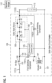
- FIG. 1 represents a perspective view of a solid-state circuit breaker 105 in accordance with an exemplary embodiment of the present invention.
- the solid-state circuit breaker 105 works by replacing the traditional moving parts of an electromechanical circuit breaker with power electronics and advanced software algorithms that control the power and can interrupt extreme currents faster than ever before.
- Solid-state circuit breakers are power semiconductor-based protection apparatuses, with no moving parts for fault current interruption.
- the response time of semiconductor devices is several orders of magnitude shorter than that of the electromechanical mechanisms typical of conventional circuit breakers.
- semiconductor devices can interrupt the flow of electrical charges without arcing.
- semiconductor-based circuit breakers can limit the let-through energy and arc hazard exposure in the event of a fault by multiple orders of magnitude.
- power semiconductor devices can execute a much higher number of operations. This translates into a greatly increased lifetime for circuit breakers.
- semiconductor devices have no moving parts, they operate without making any noise.
- semiconductor-based circuit breakers offer several additional benefits that may be application-specific.
- the solid-state circuit breaker 105 has advantages over traditional mechanical circuit breakers such as fast switching speed, minimum arcing, less moving parts etc. However, some issues also arise with the advantages of solid-state switching. One issue is switching off highly inductive load. Because of the fast switching speed, the inductive load generates high recovery voltage back to the solid-state circuit breaker 105. If not handled properly, the high recovery voltage may damage the solid-state components. This invention presents a way to discharge the high recovery voltage that can fit into small residential style circuit breakers.
- the solid-state circuit breaker 105 includes an actuator coil 107 and a second switching component 110(2) to discharge and dissipate a recovery voltage 112 associated with an inductive load 115 in accordance with an exemplary embodiment of the present invention.
- the second switching component 110(2) is a triode for alternating current (TRIAC), a silicon-controlled rectifier (SCR) or a metal-oxide-semiconductor field-effect transistor (MOSFET).
- TRIAC triode for alternating current
- SCR silicon-controlled rectifier
- MOSFET metal-oxide-semiconductor field-effect transistor
- the solid-state circuit breaker 105 is configured to feed current to the inductive load 115.
- the solid-state circuit breaker 105 comprises line-in and line-out terminals 117(1-2).
- the recovery voltage 112 occurs, it is configured to discharge through a current path that comprises the second switching component 110(2) and the actuator coil 107.
- the second switching component 110(2) is optional.
- the solid-state circuit breaker 105 further comprises a solid-state device 120 configured between the line-in and line-out terminals 117(1-2).
- the solid-state circuit breaker 105 further comprises an air-gap forming apparatus 122 between the line-in and line-out terminals 117(1-2) and coupled in series with the solid-state device 120 to complete a current conducting path.
- the solid-state circuit breaker 105 further comprises a sensing and control unit 125 that is provided across a connection point 135 after an air gap and a neutral 127 to control a gate 130 of the solid-state device 120.
- the solid-state circuit breaker 105 further comprises a first switching component 110(1) coupled in series with the actuator coil 107 across the connection point 135 after an air gap formed by the air-gap forming apparatus 122 and the neutral 127 such that the sensing and control unit 125 to control a gate 137 of the first switching component 110(1).
- the first switching component 110(1) is a triode for alternating current (TRIAC), a silicon-controlled rectifier (SCR) or a metal-oxide-semiconductor field-effect transistor (MOSFET).
- the solid-state circuit breaker 105 further comprises the second switching component 110(2) coupled between the line-out terminal 117(2) and a terminal 140 between the actuator coil 107 and the first switching component 110(1) such that the sensing and control unit 125 to control a gate 145 of the second switching component 110(2).
- the actuator coil 107 is configured to discharge and dissipate the recovery voltage 112.
- the gate 145 of the second switching component 110(2) is turned ON at the same time as the gate 130 of the solid-state device 120 is turned OFF.
- a recovery current from the recovery voltage 112 is high enough to allow the actuator coil 107 to open an air gap 150 via the air-gap forming apparatus 122.
- the recovery current is not high enough to open the air gap, the first switching component 110(1) is still turned ON after a short delay and the air gap will be open.
- the actuator coil 107 is used to discharge and dissipate the recovery voltage 112.
- the second switching component 110(2) such as TRIAC, SCR or MOSFET is added to the first switching component 110(1).
- the gate 145 of the second switching component 110(2) is turned ON at the same time as the gate 130 of the solid-state device 120 is turned OFF.
- the recovery voltage 112 can discharge through a current path that comprises of the second switching component 110(2) and the actuator coil 107.
- the actuator coil 107 don't degrade with usage, and hence can handle frequent usage as required in residential applications. Also, although it is large in physical size, the actuator coil 107 is already a component in the breaker 105. Therefore, it doesn't take any additional spaces as the capacitors do, and still allows small form factor as required in residential applications. It needs to be mentioned that the current from the recovery voltage may be high enough to allow the actuator to open the air gap. In case the recovery current is not high enough to open the air gap, the first switching component 110(1) is still turned ON after a short delay as explained previously and the air gap will be open.
- suppressing components such as a metal-oxide varistor (MOV) and a transient-voltage-suppression (TVS) diode can be used.
- MOV metal-oxide varistor
- TVS transient-voltage-suppression
- the turning ON threshold of such component is selected to be lower than the max voltage withstand of a solid-state component with a safety margin. If the recovery voltage is higher than the turning ON threshold of suppressing components, the recovery voltage is discharged through them and does not damage the solid-state components.
- Suppressing components are also used directly across main solid-state components. The drawback of such suppressing components is that they degrade from use to use so they cannot be repetitively daily used as required in residential applications.
- a capacitor can be used in the place of suppressing components.
- the capacitor and the inductive load form a circuit that allows the recovery voltage to discharge and dissipate.
- the drawback of the capacitor approach is that to handle various loads the capacitor needs to have high capacitance, voltage rating and current rating. And such capacitors are normally large in physical size so do not fit into the small form factor of residential circuit breakers.
- FIG. 2 it illustrates a schematic of a solid-state circuit breaker 205 including an actuator coil 207 and a capacitor 209 to discharge and dissipate a recovery voltage 212 associated with an inductive load 215 in accordance with an exemplary embodiment of the present invention.
- the actuator coil 207 is used in combination with one or more capacitors in parallel or in series to best match with loads.
- the capacitor 209 does not need to be as big as if using capacitors alone, because the actuator coil 207 can work as dissipation component.
- a second switching component 210(2) is optional.
- the solid-state circuit breaker 205 further comprises a solid-state device 220 configured between the line-in and line-out terminals 217(1-2).
- the solid-state circuit breaker 205 further comprises an air-gap forming apparatus 222 between the line-in and line-out terminals 217(1-2) and coupled in series with the solid-state device 220 to complete a current conducting path.
- the solid-state circuit breaker 205 further comprises a sensing and control unit 225 that is provided across the line-in, line-out terminals 217(1-2) and a neutral 227 to control a gate 230 of the solid-state device 220.
- the solid-state circuit breaker 205 further comprises a first switching component 210(1) coupled in series with the actuator coil 207 across a connection point 235 after an air gap 250 formed by the air-gap forming apparatus 222 and the neutral 227 such that the sensing and control unit 225 to control a gate 237 of the first switching component 210(1).
- FIG. 3 it illustrates a schematic of a solid-state circuit breaker 305 including an actuator coil 307 and a suppressing component 309 to discharge and dissipate a recovery voltage 312 associated with an inductive load 315 in accordance with an exemplary embodiment of the present invention.
- the actuator coil 307 is used in combination with the suppressing component 309 such as a metal-oxide varistor (MOV) and a transient-voltage-suppression (TVS) diode.
- the turn ON threshold of the suppression component 309 can be selected as high as possible in order to provide extra protection under surge type abnormal conditions.
- the actuator coil 307 handles the recovery voltage as described above.
- the solid-state circuit breaker 305 further comprises a solid-state device 320 configured between the line-in and line-out terminals 317(1-2).
- the solid-state circuit breaker 305 further comprises an air-gap forming apparatus 322 between the line-in and line-out terminals 317(1-2) and coupled in series with the solid-state device 320 to complete a current conducting path.
- the solid-state circuit breaker 305 further comprises a sensing and control unit 325 that is provided across the line-in, line-out terminals 317(1-2) and a neutral 327 to control a gate 330 of the solid-state device 320.
- the solid-state circuit breaker 305 further comprises a first switching component 310(1) coupled in series with the actuator coil 307 across a connection point 335 after an air gap formed by the air-gap forming apparatus 322 and the neutral 327 such that the sensing and control unit 325 to control a gate 337 of the first switching component 310(1).
- the solid-state circuit breaker 305 further comprises a second switching component 310(2) coupled between the line-out terminal 317(2) and a terminal 340 between the actuator coil 307 and the first switching component 310(1).
- This invention uses existing large and sturdy component that is already in the breaker instead of adding other large components. Therefore, it can fit into smaller form factors such as residential.
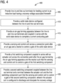
- FIG. 4 illustrates a schematic view of a flow chart of a method of discharging and dissipating a recovery voltage in a solid-state circuit breaker with an inductive load in accordance with an exemplary embodiment of the present invention.
- the method 400 comprises a step 405 of providing line-in and line-out terminals for feeding current to an inductive load having a recovery voltage associated therewith.
- the method 400 further comprises a step 410 of providing a solid-state device configured between the line-in and line-out terminals.
- the method 400 further comprises a step 415 of providing an air-gap forming apparatus between the line-in and line-out terminals and coupled in series with the solid-state device to complete a current conducting path.
- the method 400 further comprises a step 420 of providing a sensing and control unit is provided across the line-in, line-out terminals and a neutral to control a gate of the solid-state device.
- the method 400 further comprises a step 425 of providing a first switching component coupled in series with an actuator coil across a connection point after an air gap formed by the air-gap forming apparatus and the neutral such that the sensing and control unit to control a gate of the first switching component.
- the method 400 further comprises a step 430 of providing a second switching component coupled between a line-out terminal and a terminal between the actuator coil and the first switching component such that the sensing and control unit to control a gate of the second switching component.
- the actuator coil is configured to discharge and dissipate the recovery voltage.
- triode for alternating current (TRIAC) based first and second switching components are described here a range of one or more other switching components or other forms of switching components are also contemplated by the present invention.
- other types of switching components may be implemented based on one or more features presented above without deviating from the spirit of the present invention.
- MOSFETs metal-oxide-semiconductor field-effect transistors
- 2 diodes based solid-state device While particular embodiments are described in terms of these main power solid state components, the techniques described herein are not limited to such a structure but can also be used with other solid-state components.
- any examples or illustrations given herein are not to be regarded in any way as restrictions on, limits to, or express definitions of, any term or terms with which they are utilized. Instead, these examples or illustrations are to be regarded as being described with respect to one particular embodiment and as illustrative only. Those of ordinary skill in the art will appreciate that any term or terms with which these examples or illustrations are utilized will encompass other embodiments which may or may not be given therewith or elsewhere in the specification and all such embodiments are intended to be included within the scope of that term or terms.
Landscapes
- Emergency Protection Circuit Devices (AREA)
- Driving Mechanisms And Operating Circuits Of Arc-Extinguishing High-Tension Switches (AREA)
Claims (15)
- Festkörperschutzschalter (105), der dazu ausgelegt ist, Strom an eine induktive Last (115) mit einer damit assoziierten Wiederherstellungsspannung (112) zuzuführen, wobei der Festkörperschutzschalter (105) Folgendes umfasst:einen Eingangs- und einen Ausgangsanschluss (117(1-2));eine Festkörpervorrichtung (120), die zwischen dem Eingangs- und dem Ausgangsanschluss (117(1-2)) ausgebildet ist;eine Luftspaltbildungseinrichtung (122) zwischen dem Eingangs- und dem Ausgangsanschluss (117(1-2)), die mit der Festkörpervorrichtung (120) in Reihe geschaltet ist, um einen Stromleitungspfad zu vervollständigen; dadurch gekennzeichnet, dass der Festkörperschutzschalter ferner Folgendes umfasst:eine Erfassungs- und Steuereinheit (125), die zwischen einem Verbindungspunkt (135) nach einem Luftspalt und einem Neutralleiter (127) bereitgestellt ist, um ein Gate (130) der Festkörpervorrichtung (120) zu steuern;eine erste Schaltkomponente (110(1)), die zwischen dem Verbindungspunkt (135) nach dem Luftspalt und dem Neutralleiter (127) mit einer Aktuatorspule (107) in Reihe geschaltet ist, sodass die Erfassungs- und Steuereinheit (125) ein Gate (137) der ersten Schaltkomponente (110(1)) steuert; undeine zweite Schaltkomponente (110(2)), die zwischen dem Ausgangsanschluss (117(2)) und einem Anschluss (140) zwischen der Aktuatorspule (107) und der ersten Schaltkomponente (110(1)) gekoppelt ist, sodass die Erfassungs- und Steuereinheit (125) ein Gate (145) der zweiten Schaltkomponente (110(2)) steuert, wobei die Aktuatorspule (107) dazu ausgelegt ist, die Wiederherstellungsspannung (112) zu entladen und abzuleiten.
- Festkörperschutzschalter nach Anspruch 1, wobei die erste Schaltkomponente (110(1)) eine Triode für Wechselstrom (TRIAC), ein siliziumgesteuerter Gleichrichter (SCR) oder ein MetallOxid-Halbleiter-Feldeffekttransistor (MOSFET) ist.
- Festkörperschutzschalter nach Anspruch 2, wobei die zweite Schaltkomponente (110(2)) eine Triode für Wechselstrom (TRIAC), ein siliziumgesteuerter Gleichrichter (SCR) oder ein MetallOxid-Halbleiter-Feldeffekttransistor (MOSFET) ist.
- Festkörperschutzschalter nach Anspruch 1, wobei während des Ausschaltens das Gate (145) der zweiten Schaltkomponente (110(2)) gleichzeitig mit dem Ausschalten des Gate (130) der Festkörpervorrichtung (120) eingeschaltet wird.
- Festkörperschutzschalter nach Anspruch 4, wobei, wenn die Wiederherstellungsspannung (112) auftritt, sie dazu ausgelegt ist, sich über einen Strompfad zu entladen, der die zweite Schaltkomponente (110(2)) und die Aktuatorspule (107) umfasst.
- Festkörperschutzschalter nach Anspruch 5, wobei ein Wiederherstellungsstrom aus der Rückgewinnungsspannung (112) hoch genug ist, um zu gestatten, dass die Aktuatorspule (107) einen Luftspalt über die Luftspaltbildungseinrichtung (122) öffnet;
wobei optional, falls der Rückgewinnungsstrom nicht hoch genug ist, um den Luftspalt zu öffnen, die erste Schaltkomponente (110(1)) nach einer kurzen Verzögerung immer noch eingeschaltet wird und der Luftspalt offen sein wird. - Festkörperschutzschalter nach Anspruch 1, wobeia) die Aktuatorspule (107) in Kombination mit einem oder mehreren Kondensatoren in Parallel- oder Reihenschaltung verwendet wird, um am besten mit Lasten übereinzustimmen; oderb) die zweite Schaltkomponente (110(2)) optional ist; oderc) die Aktuatorspule (107) in Kombination mit einer Unterdrückungskomponente (309) verwendet wird, die einen MetallOxid-Varistor (MOV) und eine Transientenspannungsunterdrückungs(TVS)-Diode beinhaltet.
- Verfahren zum Zuführen von Strom an eine induktive Last (115) mit einer damit assoziierten Wiederherstellungsspannung (112), wobei das Verfahren Folgendes umfasst:Bereitstellen eines Eingangs- und eines Ausgangsanschlusses (117(1-2));Bereitstellen einer Festkörpervorrichtung (120), die zwischen dem Eingangs- und dem Ausgangsanschluss (117(1-2)) ausgebildet ist;Bereitstellen einer Luftspaltbildungseinrichtung (122) zwischen dem Eingangs- und dem Ausgangsanschluss (117(1-2)), die mit der Festkörpervorrichtung (120) in Reihe geschaltet ist, um einen Stromleitungspfad zu vervollständigen;Bereitstellen einer Erfassungs- und Steuereinheit (125) zwischen einem Verbindungspunkt (135) nach einem Luftspalt und einem Neutralleiter (127), um ein Gate (130) der Festkörpervorrichtung (120) zu steuern;Bereitstellen einer ersten Schaltkomponente (110(1)), die zwischen dem Verbindungspunkt (135) nach dem Luftspalt und dem Neutralleiter (127) mit einer Aktuatorspule (107) in Reihe geschaltet ist, sodass die Erfassungs- und Steuereinheit (125) ein Gate (137) der ersten Schaltkomponente (110(1)) steuert; undBereitstellen einer zweiten Schaltkomponente (110(2)), die zwischen dem Ausgangsanschluss (117(2)) und einem Anschluss (140) zwischen der Aktuatorspule (107) und der ersten Schaltkomponente (110(1)) gekoppelt ist, sodass die Erfassungs- und Steuereinheit (125) ein Gate (145) der zweiten Schaltkomponente (110(2)) steuert, wobei die Aktuatorspule (107) dazu ausgelegt ist, die Wiederherstellungsspannung (112) zu entladen und abzuleiten.
- Verfahren nach Anspruch 8, wobei die erste Schaltkomponente (110(1)) eine Triode für Wechselstrom (TRIAC), ein siliziumgesteuerter Gleichrichter (SCR) oder ein Metall-Oxid-Halbleiter-Feldeffekttransistor (MOSFET) ist.
- Verfahren nach Anspruch 9, wobei die zweite Schaltkomponente (110(2)) eine Triode für Wechselstrom (TRIAC), ein siliziumgesteuerter Gleichrichter (SCR) oder ein MetallOxid-Halbleiter-Feldeffekttransistor (MOSFET) ist.
- Verfahren nach Anspruch 8, wobei während des Ausschaltens das Gate (145) der zweiten Schaltkomponente (110(2)) gleichzeitig mit dem Ausschalten des Gate (130) der Festkörpervorrichtung (120) eingeschaltet wird.
- Verfahren nach Anspruch 11, wobei, wenn die Wiederherstellungsspannung (112) auftritt, sie dazu ausgelegt ist, sich über einen Strompfad zu entladen, der die zweite Schaltkomponente (110(2)) und die Aktuatorspule (107) umfasst.
- Verfahren nach Anspruch 12, wobei ein Wiederherstellungsstrom aus der Rückgewinnungsspannung (112) hoch genug ist, um zu gestatten, dass die Aktuatorspule (107) einen Luftspalt über die Luftspaltbildungseinrichtung (122) öffnet.
- Verfahren nach Anspruch 13, wobei, falls der Rückgewinnungsstrom nicht hoch genug ist, um den Luftspalt zu öffnen, die erste Schaltkomponente (110(1)) nach einer kurzen Verzögerung immer noch eingeschaltet wird und der Luftspalt offen sein wird.
- Verfahren nach Anspruch 8, wobeia) die Aktuatorspule (107) in Kombination mit einem oder mehreren Kondensatoren in Parallel- oder Reihenschaltung verwendet wird, um am besten mit Lasten übereinzustimmen; oderb) die zweite Schaltkomponente (110(2)) optional ist; oderc) die Aktuatorspule (107) in Kombination mit einer Unterdrückungskomponente (309) verwendet wird, die einen MetallOxid-Varistor (MOV) und eine Transientenspannungsunterdrückungs(TVS)-Diode beinhaltet.
Applications Claiming Priority (2)
| Application Number | Priority Date | Filing Date | Title |
|---|---|---|---|
| US17/227,865 US11398724B1 (en) | 2021-04-28 | 2021-04-28 | Solid-state circuit breaker configured to discharge and dissipate recovery voltage |
| PCT/US2022/021627 WO2022231735A1 (en) | 2021-04-28 | 2022-03-24 | Solid-state circuit breaker configured to discharge and dissipate recovery voltage |
Publications (2)
| Publication Number | Publication Date |
|---|---|
| EP4298701A1 EP4298701A1 (de) | 2024-01-03 |
| EP4298701B1 true EP4298701B1 (de) | 2025-04-30 |
Family
ID=81308032
Family Applications (1)
| Application Number | Title | Priority Date | Filing Date |
|---|---|---|---|
| EP22716650.1A Active EP4298701B1 (de) | 2021-04-28 | 2022-03-24 | Zur entladung und abführung von rückgewinnungsspannung konfigurierter festkörperschutzschalter |
Country Status (5)
| Country | Link |
|---|---|
| US (1) | US11398724B1 (de) |
| EP (1) | EP4298701B1 (de) |
| ES (1) | ES3037131T3 (de) |
| MX (1) | MX2023012667A (de) |
| WO (1) | WO2022231735A1 (de) |
Families Citing this family (11)
| Publication number | Priority date | Publication date | Assignee | Title |
|---|---|---|---|---|
| WO2020252561A1 (en) * | 2019-06-17 | 2020-12-24 | Smartd Technologies Inc. | Dynamic balancing of transistors |
| US12469661B2 (en) * | 2023-03-21 | 2025-11-11 | Siemens Industry, Inc. | DC solid-state circuit breaker with fail-safe redundancy via double power electronics and overvoltage protection |
| US12316095B2 (en) | 2023-03-31 | 2025-05-27 | Siemens Industry, Inc. | Solid-state circuit breaker having a sealed vacuum gap section for providing an intrinsic safe operation |
| CN119446855A (zh) * | 2023-07-28 | 2025-02-14 | 施耐德电气(中国)有限公司 | 固态断路器 |
| US20250069837A1 (en) * | 2023-08-24 | 2025-02-27 | Siemens Industry, Inc. | End of life monitoring for a solid-state circuit breaker |
| US12573567B2 (en) | 2023-09-26 | 2026-03-10 | Siemens Industry, Inc. | Semiconductor-based DC transfer switch |
| US12322952B2 (en) * | 2023-09-26 | 2025-06-03 | Siemens Industry, Inc. | DC solid state circuit breakers for bidirectional applications |
| US12362121B2 (en) * | 2023-11-06 | 2025-07-15 | Hamilton Sundstrand Corporation | Solid state parallel arc isolating device |
| US12531404B2 (en) | 2023-12-05 | 2026-01-20 | International Business Machines Corporation | Programmable power dissipation-controlled electronic circuit breaker for high voltage distribution |
| US12587183B2 (en) * | 2024-03-27 | 2026-03-24 | Siemens Industry, Inc. | Solid-state aided airgap for dc circuit breakers |
| CN120150064B (zh) * | 2025-05-13 | 2025-08-01 | 湖南大学 | 一种含限压保护电路直流固态断路器的控制方法 |
Family Cites Families (9)
| Publication number | Priority date | Publication date | Assignee | Title |
|---|---|---|---|---|
| US5170310A (en) * | 1990-11-29 | 1992-12-08 | Square D Company | Fail-resistant solid state interruption system |
| US6671150B2 (en) * | 2001-11-07 | 2003-12-30 | Eaton Corporation | Circuit breaker for detecting an excessive voltage and tripping responsive thereto |
| CN203787934U (zh) * | 2014-01-27 | 2014-08-20 | 上海誉煊电子技术有限公司 | 带冗余装置的多功能防火短路保护器 |
| CN110768650A (zh) * | 2018-07-27 | 2020-02-07 | 台达电子工业股份有限公司 | 异常电压保护装置及其操作方法 |
| US11349296B2 (en) * | 2018-10-01 | 2022-05-31 | Intelesol, Llc | Solid-state circuit interrupters |
| US11373831B2 (en) * | 2019-05-18 | 2022-06-28 | Amber Solutions, Inc. | Intelligent circuit breakers |
| US11791620B2 (en) * | 2019-09-03 | 2023-10-17 | Atom Power, Inc. | Solid-state circuit breaker with self-diagnostic, self-maintenance, and self-protection capabilities |
| WO2021046097A1 (en) * | 2019-09-03 | 2021-03-11 | Atom Power, Inc. | Solid-state circuit breaker with self-diagnostic, self-maintenance, and self-protection capabilities |
| US11368010B2 (en) * | 2020-01-17 | 2022-06-21 | Eaton Intelligent Power Limited | Solid state circuit interrupter with solid state interlocking mechanism |
-
2021
- 2021-04-28 US US17/227,865 patent/US11398724B1/en active Active
-
2022
- 2022-03-24 ES ES22716650T patent/ES3037131T3/es active Active
- 2022-03-24 MX MX2023012667A patent/MX2023012667A/es unknown
- 2022-03-24 EP EP22716650.1A patent/EP4298701B1/de active Active
- 2022-03-24 WO PCT/US2022/021627 patent/WO2022231735A1/en not_active Ceased
Also Published As
| Publication number | Publication date |
|---|---|
| WO2022231735A1 (en) | 2022-11-03 |
| MX2023012667A (es) | 2023-11-07 |
| US11398724B1 (en) | 2022-07-26 |
| CA3212224A1 (en) | 2022-11-03 |
| ES3037131T3 (en) | 2025-09-29 |
| EP4298701A1 (de) | 2024-01-03 |
Similar Documents
| Publication | Publication Date | Title |
|---|---|---|
| EP4298701B1 (de) | Zur entladung und abführung von rückgewinnungsspannung konfigurierter festkörperschutzschalter | |
| US10811867B2 (en) | Hybrid air-gap / solid-state circuit breaker | |
| US9947496B2 (en) | Circuit breaker with hybrid switch | |
| US10978259B2 (en) | Circuit breaker | |
| CN106099841A (zh) | Dc电路断路器和使用的方法 | |
| US20240305086A1 (en) | Dc solid-state circuit breaker with a solid-state aided airgap that provides a fail-safe mechanism | |
| US11984290B2 (en) | Circuit breaker | |
| US20230361560A1 (en) | Electronic circuit breaker configured to provide a fail-safe mode | |
| CN115412079A (zh) | 电子配电器 | |
| AU760489B2 (en) | An apparatus for limiting an electrical current | |
| CA3212224C (en) | Solid-state circuit breaker configured to discharge and dissipate recovery voltage | |
| EP2579054A1 (de) | Automatisches und selbsterhaltendes elektronisches system zur frühen erkennung von kurzschlüssen | |
| GB2615368A (en) | Circuit breaker | |
| KR102801941B1 (ko) | 차단기 | |
| US20250309880A1 (en) | Solid-state aided airgap for dc circuit breakers | |
| HK40035799B (en) | Hybrid air-gap/solid-state circuit breaker | |
| HK40035799A (en) | Hybrid air-gap/solid-state circuit breaker | |
| HK40001782B (en) | Hybrid air-gap / solid-state circuit breaker | |
| HK40001782A (en) | Hybrid air-gap / solid-state circuit breaker |
Legal Events
| Date | Code | Title | Description |
|---|---|---|---|
| STAA | Information on the status of an ep patent application or granted ep patent |
Free format text: STATUS: UNKNOWN |
|
| STAA | Information on the status of an ep patent application or granted ep patent |
Free format text: STATUS: THE INTERNATIONAL PUBLICATION HAS BEEN MADE |
|
| PUAI | Public reference made under article 153(3) epc to a published international application that has entered the european phase |
Free format text: ORIGINAL CODE: 0009012 |
|
| STAA | Information on the status of an ep patent application or granted ep patent |
Free format text: STATUS: REQUEST FOR EXAMINATION WAS MADE |
|
| 17P | Request for examination filed |
Effective date: 20230925 |
|
| AK | Designated contracting states |
Kind code of ref document: A1 Designated state(s): AL AT BE BG CH CY CZ DE DK EE ES FI FR GB GR HR HU IE IS IT LI LT LU LV MC MK MT NL NO PL PT RO RS SE SI SK SM TR |
|
| DAV | Request for validation of the european patent (deleted) | ||
| DAX | Request for extension of the european patent (deleted) | ||
| GRAP | Despatch of communication of intention to grant a patent |
Free format text: ORIGINAL CODE: EPIDOSNIGR1 |
|
| STAA | Information on the status of an ep patent application or granted ep patent |
Free format text: STATUS: GRANT OF PATENT IS INTENDED |
|
| RAP3 | Party data changed (applicant data changed or rights of an application transferred) |
Owner name: SIEMENS INDUSTRY, INC. |
|
| INTG | Intention to grant announced |
Effective date: 20241016 |
|
| GRAS | Grant fee paid |
Free format text: ORIGINAL CODE: EPIDOSNIGR3 |
|
| GRAA | (expected) grant |
Free format text: ORIGINAL CODE: 0009210 |
|
| STAA | Information on the status of an ep patent application or granted ep patent |
Free format text: STATUS: THE PATENT HAS BEEN GRANTED |
|
| P01 | Opt-out of the competence of the unified patent court (upc) registered |
Free format text: CASE NUMBER: APP_11501/2025 Effective date: 20250310 |
|
| AK | Designated contracting states |
Kind code of ref document: B1 Designated state(s): AL AT BE BG CH CY CZ DE DK EE ES FI FR GB GR HR HU IE IS IT LI LT LU LV MC MK MT NL NO PL PT RO RS SE SI SK SM TR |
|
| REG | Reference to a national code |
Ref country code: CH Ref legal event code: EP Ref country code: GB Ref legal event code: FG4D |
|
| REG | Reference to a national code |
Ref country code: DE Ref legal event code: R096 Ref document number: 602022013907 Country of ref document: DE |
|
| REG | Reference to a national code |
Ref country code: IE Ref legal event code: FG4D |
|
| REG | Reference to a national code |
Ref country code: NL Ref legal event code: MP Effective date: 20250430 |
|
| REG | Reference to a national code |
Ref country code: AT Ref legal event code: MK05 Ref document number: 1791006 Country of ref document: AT Kind code of ref document: T Effective date: 20250430 |
|
| REG | Reference to a national code |
Ref country code: ES Ref legal event code: FG2A Ref document number: 3037131 Country of ref document: ES Kind code of ref document: T3 Effective date: 20250929 |
|
| PG25 | Lapsed in a contracting state [announced via postgrant information from national office to epo] |
Ref country code: FI Free format text: LAPSE BECAUSE OF FAILURE TO SUBMIT A TRANSLATION OF THE DESCRIPTION OR TO PAY THE FEE WITHIN THE PRESCRIBED TIME-LIMIT Effective date: 20250430 Ref country code: PT Free format text: LAPSE BECAUSE OF FAILURE TO SUBMIT A TRANSLATION OF THE DESCRIPTION OR TO PAY THE FEE WITHIN THE PRESCRIBED TIME-LIMIT Effective date: 20250901 |
|
| REG | Reference to a national code |
Ref country code: LT Ref legal event code: MG9D |
|
| PG25 | Lapsed in a contracting state [announced via postgrant information from national office to epo] |
Ref country code: NO Free format text: LAPSE BECAUSE OF FAILURE TO SUBMIT A TRANSLATION OF THE DESCRIPTION OR TO PAY THE FEE WITHIN THE PRESCRIBED TIME-LIMIT Effective date: 20250730 Ref country code: GR Free format text: LAPSE BECAUSE OF FAILURE TO SUBMIT A TRANSLATION OF THE DESCRIPTION OR TO PAY THE FEE WITHIN THE PRESCRIBED TIME-LIMIT Effective date: 20250731 |
|
| PG25 | Lapsed in a contracting state [announced via postgrant information from national office to epo] |
Ref country code: NL Free format text: LAPSE BECAUSE OF FAILURE TO SUBMIT A TRANSLATION OF THE DESCRIPTION OR TO PAY THE FEE WITHIN THE PRESCRIBED TIME-LIMIT Effective date: 20250430 Ref country code: PL Free format text: LAPSE BECAUSE OF FAILURE TO SUBMIT A TRANSLATION OF THE DESCRIPTION OR TO PAY THE FEE WITHIN THE PRESCRIBED TIME-LIMIT Effective date: 20250430 |
|
| PG25 | Lapsed in a contracting state [announced via postgrant information from national office to epo] |
Ref country code: BG Free format text: LAPSE BECAUSE OF FAILURE TO SUBMIT A TRANSLATION OF THE DESCRIPTION OR TO PAY THE FEE WITHIN THE PRESCRIBED TIME-LIMIT Effective date: 20250430 |
|
| PG25 | Lapsed in a contracting state [announced via postgrant information from national office to epo] |
Ref country code: HR Free format text: LAPSE BECAUSE OF FAILURE TO SUBMIT A TRANSLATION OF THE DESCRIPTION OR TO PAY THE FEE WITHIN THE PRESCRIBED TIME-LIMIT Effective date: 20250430 |
|
| PG25 | Lapsed in a contracting state [announced via postgrant information from national office to epo] |
Ref country code: AT Free format text: LAPSE BECAUSE OF FAILURE TO SUBMIT A TRANSLATION OF THE DESCRIPTION OR TO PAY THE FEE WITHIN THE PRESCRIBED TIME-LIMIT Effective date: 20250430 |
|
| PG25 | Lapsed in a contracting state [announced via postgrant information from national office to epo] |
Ref country code: RS Free format text: LAPSE BECAUSE OF FAILURE TO SUBMIT A TRANSLATION OF THE DESCRIPTION OR TO PAY THE FEE WITHIN THE PRESCRIBED TIME-LIMIT Effective date: 20250731 |
|
| PG25 | Lapsed in a contracting state [announced via postgrant information from national office to epo] |
Ref country code: IS Free format text: LAPSE BECAUSE OF FAILURE TO SUBMIT A TRANSLATION OF THE DESCRIPTION OR TO PAY THE FEE WITHIN THE PRESCRIBED TIME-LIMIT Effective date: 20250830 |
|
| PG25 | Lapsed in a contracting state [announced via postgrant information from national office to epo] |
Ref country code: LV Free format text: LAPSE BECAUSE OF FAILURE TO SUBMIT A TRANSLATION OF THE DESCRIPTION OR TO PAY THE FEE WITHIN THE PRESCRIBED TIME-LIMIT Effective date: 20250430 |
|
| PG25 | Lapsed in a contracting state [announced via postgrant information from national office to epo] |
Ref country code: SM Free format text: LAPSE BECAUSE OF FAILURE TO SUBMIT A TRANSLATION OF THE DESCRIPTION OR TO PAY THE FEE WITHIN THE PRESCRIBED TIME-LIMIT Effective date: 20250430 Ref country code: DK Free format text: LAPSE BECAUSE OF FAILURE TO SUBMIT A TRANSLATION OF THE DESCRIPTION OR TO PAY THE FEE WITHIN THE PRESCRIBED TIME-LIMIT Effective date: 20250430 |
|
| PG25 | Lapsed in a contracting state [announced via postgrant information from national office to epo] |
Ref country code: CZ Free format text: LAPSE BECAUSE OF FAILURE TO SUBMIT A TRANSLATION OF THE DESCRIPTION OR TO PAY THE FEE WITHIN THE PRESCRIBED TIME-LIMIT Effective date: 20250430 |
|
| PG25 | Lapsed in a contracting state [announced via postgrant information from national office to epo] |
Ref country code: EE Free format text: LAPSE BECAUSE OF FAILURE TO SUBMIT A TRANSLATION OF THE DESCRIPTION OR TO PAY THE FEE WITHIN THE PRESCRIBED TIME-LIMIT Effective date: 20250430 |
|
| PG25 | Lapsed in a contracting state [announced via postgrant information from national office to epo] |
Ref country code: SK Free format text: LAPSE BECAUSE OF FAILURE TO SUBMIT A TRANSLATION OF THE DESCRIPTION OR TO PAY THE FEE WITHIN THE PRESCRIBED TIME-LIMIT Effective date: 20250430 |
|
| REG | Reference to a national code |
Ref country code: DE Ref legal event code: R097 Ref document number: 602022013907 Country of ref document: DE |
|
| PLBE | No opposition filed within time limit |
Free format text: ORIGINAL CODE: 0009261 |
|
| STAA | Information on the status of an ep patent application or granted ep patent |
Free format text: STATUS: NO OPPOSITION FILED WITHIN TIME LIMIT |
|
| REG | Reference to a national code |
Ref country code: CH Ref legal event code: L10 Free format text: ST27 STATUS EVENT CODE: U-0-0-L10-L00 (AS PROVIDED BY THE NATIONAL OFFICE) Effective date: 20260311 |
|
| 26N | No opposition filed |
Effective date: 20260202 |
|
| PGFP | Annual fee paid to national office [announced via postgrant information from national office to epo] |
Ref country code: IT Payment date: 20260324 Year of fee payment: 5 |
|
| PGFP | Annual fee paid to national office [announced via postgrant information from national office to epo] |
Ref country code: FR Payment date: 20260316 Year of fee payment: 5 |