EP4300107B1 - Détection de fuite de courant pour dispositifs à semi-conducteurs - Google Patents
Détection de fuite de courant pour dispositifs à semi-conducteurs Download PDFInfo
- Publication number
- EP4300107B1 EP4300107B1 EP23178854.8A EP23178854A EP4300107B1 EP 4300107 B1 EP4300107 B1 EP 4300107B1 EP 23178854 A EP23178854 A EP 23178854A EP 4300107 B1 EP4300107 B1 EP 4300107B1
- Authority
- EP
- European Patent Office
- Prior art keywords
- solid state
- state device
- test
- leakage current
- voltage
- Prior art date
- Legal status (The legal status is an assumption and is not a legal conclusion. Google has not performed a legal analysis and makes no representation as to the accuracy of the status listed.)
- Active
Links
Images





Classifications
-
- G—PHYSICS
- G01—MEASURING; TESTING
- G01R—MEASURING ELECTRIC VARIABLES; MEASURING MAGNETIC VARIABLES
- G01R31/00—Arrangements for testing electric properties; Arrangements for locating electric faults; Arrangements for electrical testing characterised by what is being tested not provided for elsewhere
- G01R31/26—Testing of individual semiconductor devices
- G01R31/2607—Circuits therefor
- G01R31/2621—Circuits therefor for testing field effect transistors, i.e. FET's
-
- G—PHYSICS
- G01—MEASURING; TESTING
- G01R—MEASURING ELECTRIC VARIABLES; MEASURING MAGNETIC VARIABLES
- G01R31/00—Arrangements for testing electric properties; Arrangements for locating electric faults; Arrangements for electrical testing characterised by what is being tested not provided for elsewhere
- G01R31/28—Testing of electronic circuits, e.g. by signal tracer
- G01R31/2851—Testing of integrated circuits [IC]
- G01R31/2855—Environmental, reliability or burn-in testing
- G01R31/2872—Environmental, reliability or burn-in testing related to electrical or environmental aspects, e.g. temperature, humidity, vibration, nuclear radiation
- G01R31/2879—Environmental, reliability or burn-in testing related to electrical or environmental aspects, e.g. temperature, humidity, vibration, nuclear radiation related to electrical aspects, e.g. to voltage or current supply or stimuli or to electrical loads
-
- G—PHYSICS
- G01—MEASURING; TESTING
- G01R—MEASURING ELECTRIC VARIABLES; MEASURING MAGNETIC VARIABLES
- G01R31/00—Arrangements for testing electric properties; Arrangements for locating electric faults; Arrangements for electrical testing characterised by what is being tested not provided for elsewhere
- G01R31/28—Testing of electronic circuits, e.g. by signal tracer
- G01R31/317—Testing of digital circuits
- G01R31/31712—Input or output aspects
-
- G—PHYSICS
- G01—MEASURING; TESTING
- G01R—MEASURING ELECTRIC VARIABLES; MEASURING MAGNETIC VARIABLES
- G01R31/00—Arrangements for testing electric properties; Arrangements for locating electric faults; Arrangements for electrical testing characterised by what is being tested not provided for elsewhere
- G01R31/327—Testing of circuit interrupters, switches or circuit-breakers
- G01R31/3277—Testing of circuit interrupters, switches or circuit-breakers of low voltage devices, e.g. domestic or industrial devices, such as motor protections, relays, rotation switches
-
- G—PHYSICS
- G01—MEASURING; TESTING
- G01R—MEASURING ELECTRIC VARIABLES; MEASURING MAGNETIC VARIABLES
- G01R31/00—Arrangements for testing electric properties; Arrangements for locating electric faults; Arrangements for electrical testing characterised by what is being tested not provided for elsewhere
- G01R31/50—Testing of electric apparatus, lines, cables or components for short-circuits, continuity, leakage current or incorrect line connections
- G01R31/52—Testing for short-circuits, leakage current or ground faults
-
- G—PHYSICS
- G01—MEASURING; TESTING
- G01R—MEASURING ELECTRIC VARIABLES; MEASURING MAGNETIC VARIABLES
- G01R31/00—Arrangements for testing electric properties; Arrangements for locating electric faults; Arrangements for electrical testing characterised by what is being tested not provided for elsewhere
- G01R31/50—Testing of electric apparatus, lines, cables or components for short-circuits, continuity, leakage current or incorrect line connections
- G01R31/56—Testing of electric apparatus
Definitions
- the present disclosure relates to the field of current leak detection for solid state devices.
- Solid state devices such as solid state switches, are used in various applications such as in circuit breakers, e-Fuses, etc. In these types of applications, the solid state devices may remain in the same state for extended periods of time. For example, a solid state device of a circuit breaker may remain in an on state where the solid state device is conducting for years. The solid state device will turn off and close to stop conducting if there is an abnormal condition such as an overload or short circuit. Unfortunately, there is no way to test the solid state device to see if the solid state device is operating correctly and will be able to completely turn off in the event of the abnormal condition. This can result in catastrophic failures and damage.
- an abnormal condition such as an overload or short circuit.
- US 2014/0043058 A1 discloses a semiconductor module in a power system of an apparatus.
- the semiconductor module includes a semiconductor switch, a voltage applying device configured to apply a first voltage to the semiconductor switch in an off-state in a case where the apparatus is not in practical use, and a leak detecting circuit configured to detect a leak current from the semiconductor switch.
- the first voltage is equal to or higher than a rated voltage of the apparatus.
- the rated voltage of the apparatus is a rated voltage when the apparatus is in practical use.
- One embodiment relates to an apparatus according to claim 1. Another embodiment relates to a method according to claim 9.
- Solid state devices may comprise solid state switches, metal-oxide-semiconductor field-effect transistors (MOSFETs), etc.
- MOSFETs metal-oxide-semiconductor field-effect transistors
- a solid state device may transition from one of the states to another state based upon a voltage applied to a gate of the solid state device. Once the voltage of the gate reaches a threshold voltage Vth, then the solid state device may change states, such as where the solid state device is turned on and starts conducting. In certain applications, the solid state device may remain in a particular state for an extended period of time.
- This period of time could be years, such as where a solid state device of a circuit breaker is in an on state until an abnormal condition of an electric supply network occurs such as an overload or short circuit. Because the solid state device remains in one state for such a long period of time, there is no way to verify that the solid state device is operating correctly and will be able to transition states when needed such as to safely turn off when the abnormal condition occurs. This can lead to catastrophic failures and damage.
- the health and operability of the solid state device may deteriorate over time due to various reasons such as stress on the solid state device.
- One issue that can occur is that the threshold voltage Vth of the gate can drift over time, which can lead to excessive leakage current, leakage current due to a drain source on resistance (RDSon) being too low, and/or failure where the solid state device cannot switch states such as to turn off safely.
- RDSon drain source on resistance
- the solid state device may not even be able to turn off.
- High leakage currents due to this drift causes health deterioration of the apparatus comprising the solid state device, such as where there is always current flowing through the solid state device to a secondary side of the apparatus. This could lead to a high voltage condition on the secondary side that should otherwise be turned off.
- the solid state device cannot completely shut off, then the solid state device will operate similar to a current source and deliver a significant amount of current (e.g., 10 to 100 milliamps) that can cause overheating and failure due to damage from thermal overstress behavior.
- the drift of the threshold voltage Vth can occur over a long period of time, and thus the leakage current may slowly increase over time. There is currently no ability to detect this slow drift and leakage current increase in-situ during operation of the apparatus comprising the solid state device.
- a leak detection component and leak detection technique are provided.
- the leak detection component is capable of testing and monitoring a solid state device of an apparatus during operation of the apparatus in order to detect imminent or future failure of the solid state device.
- the leak detection component is capable of identifying drift of the threshold voltage Vth of the solid state device based upon a leakage current of the solid state device measured by the leak detection component.
- the leakage current is detected during operation of the apparatus (e.g., while the circuit breaker or e-Fuse is installed and operational, as opposed to in a test lab environment) by the leak detection component by applying a test voltage to a gate of the solid state device.
- the leak detection component detects a leakage current resulting from the test voltage being applied to the gate of the solid state device.
- the test voltage is less than the threshold voltage Vth of the solid state device 102 such that increased leakage current will be detected if the solid state device is operating in a degraded operating state (e.g., leakage current larger than a nanoampere range of normal/expected leakage current of a non-degraded device) due to drift of the threshold voltage Vth (e.g., the threshold voltage Vth has drifted down to a smaller value than normal). Otherwise, the test voltage would not be enough voltage to cause the solid state device, operating in a non-degraded operating state, to turn on and conduct current through the solid state device.
- a degraded operating state e.g., leakage current larger than a nanoampere range of normal/expected leakage current of a non-degraded device
- drift of the threshold voltage Vth e.g., the threshold voltage Vth has drifted down to a smaller
- various actions can be performed such as generating a warning signal of the degraded operating state (e.g., blinking a light, displaying a message, transmitting a message to a remote device, etc.).
- a warning signal of the degraded operating state e.g., blinking a light, displaying a message, transmitting a message to a remote device, etc.
- Fig. 1A illustrates a leak detection component 109 configured to dynamically monitor the operating state and health of a solid state device 102 (e.g., a device under test (DUT)) of an apparatus 100.
- the apparatus 100 comprises a voltage source 110 that is connected to a switch 112.
- the switch 112 is a battery main switch that electrically connects and disconnects the voltage source 110 from other components of the apparatus 100 such as the solid state device 102.
- the switch 112 may be connected in series with the solid state device 102 so that power from the voltage source 110 is supplied to the solid state device 102 (e.g., to a source of the solid state device 102) when the switch 112 is on (closed).
- the apparatus 100 comprises a load 114 connected in series to the switch 112 and the solid state device 102.
- the load 114 is represented by a resistance Rdisc and capacitance Cbyp for simplicity, but may comprise various components, circuitry, hardware, and/or software.
- an auxiliary current laux 120 and a voltage 116 e.g., Vfuse
- the load 114 may be in an operational state (on) or a non-operational (off) based upon a load enable signal 124 (e.g., a signal generated by software to turn on or off the load 114).
- the signal 124 may be used to control a controllable portion 115 of the load 114, such as an inverter circuit.
- a discharge circuit of the load 114 e.g., Rdisc and Cbyp
- the load 114 may generate the auxiliary current laux 120 and the voltage 116 when the load enable signal 124 is enabled to turn on the load 114 and the switch 112 is closed so that the load 114 is connected to the voltage source 110.
- a gate driver 104 may be connected to the gate of the solid state device 102.
- the gate driver 104 may be configured to drive the gate of the solid state device 102 by applying a voltage to the solid state device 102 in order to operate the solid state device 102.
- the gate driver 104 applies a voltage equal to or greater than the threshold voltage Vth of the solid state device 102, then the solid state device 102 will turn on into an operational state.
- a device enable signal 126 may be used to control the gate driver 104 to turn on or off the solid state device 102.
- the device enable signal 126 causes the gate driver 104 to apply the voltage, equal to or greater than the threshold voltage Vth of the solid state device 102, to the gate of the solid state device 102.
- the device enable signal 126 is disabled to cause the gate driver 104 to stop applying the voltage to the gate of the solid state device 102.
- the solid state device 102 will produce significant leakage current when the solid state device 102 is supposed to be in an off state even to the point of where the solid state device 102 is not able to fully turn off by applying a normally applied off-level voltage via the gate driver 104. This can cause catastrophic failure and damage to the apparatus 100, such as where a circuit breaker is unable to turn off in the event of a short circuit or other abnormal condition.
- the leak detection component 109 in combination with a dedicated gate stimulus circuit (e.g., test circuitry 108) is used to detect these indicators of degraded performance and potential failure of the solid state device 102.
- a dedicated gate stimulus circuit e.g., test circuitry 108
- the leak detection component 109 may be connected to the solid state device 102. In some embodiments, the leak detection component 109 is connected in parallel with the solid state device 102. In some embodiments, the leak detection component 109 is connected to a source and a drain of the solid state device 102. In some embodiments, a leak detection component may be implemented as a current measurement device in series with the solid state device 102. The leak detection component 109 is configured to measure a leakage current of the solid state device 102 when a test voltage is applied to the gate of the solid state device 102 during a test sequence. The test sequence is used to test the health of the solid state device 102 for determining whether the solid state device 102 is operating in a non-degraded operating state or degraded operating state. Details of the test sequence are further described in conjunction with the method 200 of Fig. 2 .
- the apparatus 100 includes test circuitry 108 configured to apply a test voltage 118 to the gate of the solid state device 102.
- the test circuitry 108 is integrated into the gate driver 104.
- the test circuitry 108 is controlled by a test enable signal 122.
- the test circuitry 108 closes a series switch 123 that is in series between a test voltage source 119 and the gate of the solid state device 102.
- Closing the series switch 123 connects the test voltage source 119 to the gate of the solid state device 102 so that that the test voltage 118 is applied to the gate of the solid state device 102.
- the test voltage 118 is less than the threshold voltage Vth. In this way, the solid state device 102 will not turn on from the test voltage 118 being applied to the gate of the solid state device 102 if the solid state device 102 is operating in a non-degraded operating state and has not experienced significant drift of the threshold voltage Vth.
- the test voltage 118 is applied to the gate of the solid state device 102 while the solid state device 102 is in an off state where the gate driver 104 is not applying a voltage to the gate of the solid state device 102.
- the leak detection component 109 measures the leakage current output through the solid state device 102 while the test voltage 118 is applied to the gate of the solid state device 102.
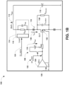
- the leak detection component 109 may measure the leakage current utilizing a capacitor 130, as illustrated by Fig. 1B .
- the capacitor 130 is connected to the solid state device 102 in parallel.
- switch 112 is closed (e.g., switch 112 is normally closed), the load 114 is disabled, and the device 102 is opened. In this way, the capacitor 130 is charged up to Vbattery. Then, the switch 112 is opened and the test voltage 118 is applied to the gate of the solid state device 102.
- a discharge rate of the capacitor 130 is proportional to the leakage current of the solid state device 102.
- an external source is used to charge the capacitor 103 or a current source may feed into a pin (e.g., pin Vfuse associated with voltage 116) while the load 114 is disabled and the switch 112 is opened.
- the leak detection component 109 measures a rate of change of a charge of the capacitor 130 over time to determine whether the rate of change of the charge of the capacitor 130 exceeds a threshold. The larger the rate of change of the charge of the capacitor 130, the larger the leakage current of the solid state device 102.
- the test sequence may include charging the capacitor 130, turning on the switch 112, and then measuring the voltage 116 across the switch 112 to identify the rate of change of the charged of the capacitor 130 over time.
- the leak detection component 109 determines that the solid state device 102 is operating in a non-degraded operating state. If the rate of change of the charge of the capacitor 130 exceeds the threshold, then the leak detection component 109 determines that the solid state device 102 is operating in a degraded operating state.
- the leak detection component 109 may generate a signal, such as a warning signal that the solid state device 102 is unhealthy, operating in the degraded operating state, and/or should be replaced (e.g., the signal may cause a light on the apparatus 100 to turn on, a message to be displayed on the apparatus 100, or a message to be transmitted to a remote device over a communication network).
- a signal such as a warning signal that the solid state device 102 is unhealthy, operating in the degraded operating state, and/or should be replaced (e.g., the signal may cause a light on the apparatus 100 to turn on, a message to be displayed on the apparatus 100, or a message to be transmitted to a remote device over a communication network).
- the leak detection component 109 may utilize other components and/or functionality than the capacitor 130 for measuring the leakage current of the solid state device 102.
- the leak detection component 109 utilizes a voltage source 140 as part of the test sequence for measuring the leakage current, as illustrated by Fig. 1C .
- the voltage source 140 may be an independent voltage source from other voltage sources of the apparatus 100 such as the voltage source 110.
- the leak detection component 109 utilizes a current source 150 as part of the test sequence for measuring the leakage current, as illustrated by Fig. 1D .
- the current source 150 may apply a current to a drain potential of a drain of the solid state device 102.
- a current through the solid state device 102 is measured to determine the leakage current of the solid state device 102.
- a leak detection component may be implemented as a current measurement device in series with the solid state device 102.
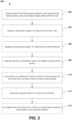
- Fig. 2 illustrates a method 200 for detecting leakage current of the solid state device 102.
- the solid state device 102 is turned on using the device enable signal 126.
- the device enable signal 126 causes the gate driver 104 to apply a voltage to the gate of the solid state device 102. The voltage is equal to or greater than the threshold voltage Vth of the solid state device 102. This causes the solid state device 102 to turn on.
- the solid state device 102 is turned on while the switch 112 is on (e.g., closed so that the voltage source 110 is connected to the load 114 and/or the solid state device 102).
- the load 114 is turned on using the load enable signal 124. In this way, the switch 112 is closed, and the solid state device 102 and the load 114 are turned on into an operational state.
- the leak detection component 109 may determine that a test sequence is to be initiated to determine whether the solid state device 102 is operating in a non-degraded operating state or a degraded operating state (e.g., a threshold amount of time has passed since a prior test sequence was performed). Accordingly, during operation 204 of method 200, the load enable signal 124 is disabled in order to turn off the load 114. In this way, the load 114 is not drawing power, such as from the voltage source 110, while off. In some embodiments, the load 114 is turned off while the switch 112 is still on (closed).
- the device enable signal 126 is disabled to turn off the solid state device 102.
- the device enable signal 126 is an input into the gate driver 104 in order to control the gate driver 104.
- Disabling the device enable signal 126 triggers the gate driver 104 to stop applying the voltage, greater than the threshold voltage Vth, to the gate of the solid state device 102, thus turning off the solid state device 102.
- the gate driver 104 provides an off-level gate driver signal to the solid state device 102.
- the switch 112 is turned off to interrupt the supply of power to the solid state device 102.
- the switch is turned off (opened) in order to interrupt the supply of power from the voltage source 110 through the load 114 to the source of the solid state device 102.
- the test sequence triggers the test circuitry 108 to apply the test voltage 118 to the gate of the solid state device 102.
- the test sequence is initiated by applying the test voltage 118 to the gate of the solid state device 102 using the test circuitry 108.
- the test voltage 118 is less than the threshold voltage Vth such that if the solid state device 102 is operating in a non-degraded operating state (e.g., experiencing little to no threshold voltage Vth drift), then the solid state device 102 will not turn on and will not generate a large leakage current.
- the test sequence of the test voltage 118 being applied to the gate of the solid state device 102 and the leak detection component 109 determining a leakage current inducted by the test voltage 118 is performed in-situ when the apparatus 100 is deployed and operational (e.g., during a power up/down sequence of a vehicle boardnet of a vehicle).
- the test voltage 118 is applied to the gate of the solid state device 102 while the solid state device 102 is in an off state where the gate driver 104 is not applying the voltage greater than the threshold voltage Vth to the gate of the solid state device 102.
- the leak detection component 109 measures the leakage current from the solid state device 102.
- the leakage current may be induced by the test voltage 118 being applied to the gate of the solid state device 102.
- Various techniques may be used to measure the leakage current or other operational properties of the solid state device 102, such as through the use of the capacitor 130 of Fig. 1B , the voltage source 140 of Fig. 1C , the current source 150 of Fig. 1D , etc.
- the leak detection component 109 measures a rate of change of a charge of the capacitor 130 over time. The leakage detection components determines the leakage current based upon the rate of change of the charge of the capacitor 130 over time.
- the leak detection component 109 determines whether the solid state device 102 is operating in a degraded operating state or a non-degraded operation state based upon the leakage current of the solid state device 102 and/or the rate of change of the charge of the capacitor 130 over time.
- the leak detection component 109 may generate a warning signal (e.g., turn on or blink a warning light of the apparatus 100, display an alert on a display of the apparatus 100, transmit the warning signal to a remote device or computer to notify a user, etc.).
- a warning signal e.g., turn on or blink a warning light of the apparatus 100, display an alert on a display of the apparatus 100, transmit the warning signal to a remote device or computer to notify a user, etc.
- Fig. 3 illustrates a timing diagram 300 associated with solid state device leak detection.
- the x-axis represents time during which the test sequence may be performed.
- the load enable signal 124 is initially enabled (high) so that the load 114 is on and operational.
- the device enable signal 126 is also initially enabled (high) so that the gate driver 104 applies a voltage to the gate of the solid state device 102.
- the voltage applied to the gate of the solid state device 102 is equal to or larger than the threshold voltage Vth 323 of the solid state device 102 (e.g., greater than 3.5V, 4.5V, or some other threshold voltage), and thus the solid state device 102 is on and operational.
- a switch enable signal 306, used to control the switch 112, is initially enabled (high) so that the switch 112 is on (closed).
- the load enable signal 124 is disabled (low) at a first point in time 316 to turn off the load 114.
- the device enable signal 126 is disabled (low) at a second point in time 317 to turn off the solid state device 102 by controlling the gate driver 104 to stop applying the voltage to the gate of the solid state device 102.
- the switch enable signal 306 is disabled (low) at a third point in time 318 so that the switch 112 is off (opened).
- the switch 112 may be turned off once the voltage 116 has reached a battery voltage 310 of the voltage source 110.
- the test enable signal 122 is enabled (high) to cause the test circuitry 108 to apply the test voltage 118 to the gate of the solid state device 102, which has a gate voltage 312.
- a rate of change 324 of a charge of the capacitor 130 is measured while the test voltage 118 is applied to the gate of the solid state device 102 in order to determine an increase in leakage current of the solid state device 102 from the test voltage 118 being applied to the gate of the solid state device 102.
- the test enable signal 122 is disabled (low) at a fifth point in time 322 to complete the test sequence.
- Fig. 4 illustrates a diagram 400 depicting various voltage threshold drifts of the solid state device 102.
- the x-axis 404 represents voltage, such as the threshold voltage Vth 406 of the solid state device 102 and a gate-source voltage bias 408 of the solid state device 102.
- the y-axis 402 represents current from the solid state device 102, such as leakage current produced before a voltage applied to the gate of the solid state device 102 reaches the threshold voltage Vth 406.
- a current curve 410 represents current from the solid state device 102 if the solid state device is operating in a non-degraded operating state. The current curve 410 shows that there is little to no leakage current before the voltage applied to the gate reaches the threshold voltage Vth 406. Once the threshold voltage Vth 406 is reached, then current from the solid state device 102 increases because the solid state device 102 is on and operational.
- the current curve 412 illustrates how leakage current from the solid state device 102 occurs before the threshold voltage Vth 406 is reached, which is indicative of a leakage current due to drift in the threshold voltage Vth 406.
- Current curve 414 illustrates critical drift in the threshold voltage Vth 406 where there is leakage current well before the threshold voltage Vth 406 is reached.
- Current curve 416 illustrates very critical drift in the threshold voltage Vth 406 where the solid state device 102 may not even be able to turn off and there is significant leakage current while the solid state device 102 is supposed to be off.
- the techniques described herein are capable of detecting these leakage currents and voltage threshold drifts during operation of the solid state device 102 in order to provide early detection and warning of imminent or potential future failures.
- the terms “component,” “module,” “system”, “interface”, and the like are generally intended to refer to a computer-related entity, either hardware, a combination of hardware and software, software, or software in execution.
- One or more components may be localized on one computer and/or distributed between two or more computers.
- the claimed subject matter may be implemented as a method, apparatus, or article of manufacture using standard programming and/or engineering techniques to produce software, firmware, hardware, or any combination thereof to control a computer to implement the disclosed subject matter.
- article of manufacture as used herein is intended to encompass a computer program accessible from any computer-readable device, carrier, or media.
- one or more of the operations described may constitute computer readable instructions stored on one or more computer readable media, which if executed by a computing device, will cause the computing device to perform the operations described.
- the order in which some or all of the operations are described should not be construed as to imply that these operations are necessarily order dependent. Alternative ordering will be appreciated by one skilled in the art having the benefit of this description. Further, it will be understood that not all operations are necessarily present in each embodiment provided herein.
- any aspect or design described herein as an "example” is not necessarily to be construed as advantageous over other aspects or designs. Rather, use of the word “example” is intended to present one possible aspect and/or implementation that may pertain to the techniques presented herein. Such examples are not necessary for such techniques or intended to be limiting. Various embodiments of such techniques may include such an example, alone or in combination with other features, and/or may vary and/or omit the illustrated example.
- first,” “second,” or the like are not intended to imply a temporal aspect, a spatial aspect, an ordering, etc. Rather, such terms are merely used as identifiers, names, etc. for features, elements, items, etc.
- a first element and a second element generally correspond to element A and element B or two different or two identical elements or the same element.
Landscapes
- Physics & Mathematics (AREA)
- General Physics & Mathematics (AREA)
- Engineering & Computer Science (AREA)
- Microelectronics & Electronic Packaging (AREA)
- Environmental & Geological Engineering (AREA)
- General Engineering & Computer Science (AREA)
- Power Engineering (AREA)
- Health & Medical Sciences (AREA)
- Toxicology (AREA)
- Computer Hardware Design (AREA)
- Testing Of Individual Semiconductor Devices (AREA)
- Investigating Or Analyzing Materials By The Use Of Electric Means (AREA)
Claims (13)
- Un montage, comprenant :un dispositif (102) à l'état solide ;un interrupteur (112) en série avec le dispositif (102) à l'état solide ;un composant (109) de détection de fuite connecté au dispositif (102) à l'état solide et comprenant un condensateur (130) monté en parallèle avec le dispositif (102) à l'état solide; etune attaque (104) de grille configurée pour attaquer une grille du dispositif (102) à l'état solide et comprenant un circuit (108) de test configuré pour appliquer une tension (118) de test à la grille du dispositif (102) à l'état solide,dans lequel la tension (118) de test est inférieure à une tension de seuil du dispositif (102) à l'état solide, etdans lequel le composant (108) de détection de fuite est configuré pour détecter un courant de fuite du dispositif (102) à l'état solide,dans lequel le condensateur (130) du composant de détection de fuite est configuré pour être chargé, lorsque l'interrupteur (112) est fermé, etdans lequel le composant (109) de détection de fuite est configuré pour détecter le courant de fuite sur la base d'un taux de variation d'une charge du condensateur (130) sur un laps de temps dépassant un seuil, lorsque l'interrupteur (112) est ouvert.
- Montage suivant la revendication 1, dans lequel le composant (109) de détection de fuite est configuré pour produire un signal sur la base du courant de fuite du dispositif (102) à l'état solide, afin d'indiquer si le dispositif (102) à l'état solide fonctionne dans un état de fonctionnement dégradé ou dans un état de fonctionnement non dégradé.
- Montage suivant la revendication 1 ou 2, dans lequel une dérive de la tension de seuil du dispositif (102) à l'état solide est déterminée sur la base du courant de fuite.
- Montage suivant l'une quelconque des revendications précédentes,dans lequel le circuit (108) de test est configuré pour appliquer la tension (118) de test à la grille du dispositif (102) à l'état solide etdans lequel le composant de détection de fuite est configuré pour détecter le courant de fuite in situ pendant le fonctionnement du montage (100) et du dispositif (102) à l'état solide.
- Montage suivant l'une quelconque des revendications précédentes, dans lequel le circuit (108) de test est configuré pour appliquer la tension (118) de test à la grille du dispositif (102) à l'état solide, alors que le dispositif (102) à l'état solide est dans un état bloqué.
- Montage suivant l'une quelconque des revendications précédentes, dans lequel le circuit (108) de test comprend un interrupteur en série pour la grille.
- Montage suivant l'une quelconque des revendications précédentes, dans lequel le circuit (108) de test comprend une source de tension qui produit la tension (118) de test.
- Montage suivant la revendication 1, dans lequel le montage (100) est un disjoncteur ou un fusible e.
- Procédé de test d'un dispositif à l'état solide, comprenant :mettre en circuit un dispositif (102) à l'état solide en utilisant un signal (126) de validation du dispositif et mettre en circuit une charge (115) en utilisant un signal (124) de validation de charge, alors qu'un interrupteur (112) est fermé ;invalider le signal (124) de validation de charge pour mettre la charge (115) hors circuit ;invalider le signal de validation (126) de dispositif pour mettre le dispositif (102) à l'état solide hors circuit ;ouvrir l'interrupteur (112) pour interrompre l'alimentation en courant du dispositif (102) à l'état solide;en réaction à l'ouverture de l'interrupteur (112), lancer une séquence de test en appliquant une tension (118) de test à une grille du dispositif (102) à semi l'état solide conducteur ;mesurer un courant de fuite du dispositif (102) à l'état solide; etdéterminer si le dispositif (102) à l'état solide fonctionne dans un état de fonctionnement dégradé sur la base du courant de fuite,dans lequel lancer la séquence de test comprend :déterminer le courant de fuite du dispositif (102) à l'état solide sur la base d'un taux de variation d'une charge d'un condensateur (130) en fonction du temps, dans lequel le condensateur (130) est monté en parallèle avec le dispositif à l'état solide; etdéterminer si le dispositif (130) à l'état solide fonctionne dans l'état de fonctionnement dégradé sur la base du courant de fuite.
- Procédé suivant la revendication 9, comprenant en outre :
déterminer une dérive de la tension de seuil du dispositif (102) à l'état solide sur la base du courant de fuite. - Procédé suivant la revendication 9, dans lequel lancer la séquence de test comprend :appliquer, par un circuit (108) de test intégré dans une attaque (104) de grille, la tension (118) de test à la grille du dispositif (102) à l'état solide, dans lequel la tension (118) de test est inférieure à une tension de seuil du dispositif (102) à l'état solide; etdéterminer si le dispositif (102) à l'état solide fonctionne dans l'état de fonctionnement dégradé sur la base du courant de fuite induit par la tension (118) de test.
- Procédé suivant l'une quelconque des revendications 10 à 11, dans lequel la séquence de test est effectuée in situ pendant le fonctionnement d'un montage (100) comprenant le dispositif (102) à l'état solide.
- Procédé suivant l'une quelconque des revendications 10 à 12, comprenant
en réaction à la détermination que le dispositif (102) à l'état solide fonctionne dans l'état de fonctionnement dégradé, produire un signal d'alerte.
Applications Claiming Priority (1)
| Application Number | Priority Date | Filing Date | Title |
|---|---|---|---|
| US17/850,713 US12146923B2 (en) | 2022-06-27 | 2022-06-27 | Current leak detection for solid state devices |
Publications (2)
| Publication Number | Publication Date |
|---|---|
| EP4300107A1 EP4300107A1 (fr) | 2024-01-03 |
| EP4300107B1 true EP4300107B1 (fr) | 2025-01-29 |
Family
ID=86764393
Family Applications (1)
| Application Number | Title | Priority Date | Filing Date |
|---|---|---|---|
| EP23178854.8A Active EP4300107B1 (fr) | 2022-06-27 | 2023-06-13 | Détection de fuite de courant pour dispositifs à semi-conducteurs |
Country Status (3)
| Country | Link |
|---|---|
| US (1) | US12146923B2 (fr) |
| EP (1) | EP4300107B1 (fr) |
| KR (1) | KR20240001684A (fr) |
Families Citing this family (2)
| Publication number | Priority date | Publication date | Assignee | Title |
|---|---|---|---|---|
| US12399793B2 (en) * | 2023-05-31 | 2025-08-26 | SanDisk Technologies, Inc. | Adaptive word line stress for leak detection in non-volatile memory |
| IT202300013689A1 (it) * | 2023-06-30 | 2024-12-30 | St Microelectronics Int Nv | Circuito di monitoraggio e corrispondente procedimento |
Citations (1)
| Publication number | Priority date | Publication date | Assignee | Title |
|---|---|---|---|---|
| JP2014035301A (ja) * | 2012-08-09 | 2014-02-24 | Toyota Motor Corp | 半導体モジュール |
Family Cites Families (37)
| Publication number | Priority date | Publication date | Assignee | Title |
|---|---|---|---|---|
| JPH03210726A (ja) * | 1990-01-12 | 1991-09-13 | Mitsubishi Electric Corp | 漏電警報機能付き配線用遮断器 |
| US6348806B1 (en) * | 1999-03-18 | 2002-02-19 | Motorola, Inc. | Method and apparatus for measuring gate leakage current in an integrated circuit |
| US6882172B1 (en) * | 2002-04-16 | 2005-04-19 | Transmeta Corporation | System and method for measuring transistor leakage current with a ring oscillator |
| US6909295B2 (en) * | 2003-09-24 | 2005-06-21 | International Business Machines Corporation | Analysis methods of leakage current luminescence in CMOS circuits |
| DE102004059643B4 (de) * | 2004-12-10 | 2009-11-12 | Infineon Technologies Ag | Gateansteuerschaltung für einen Leistungstransistor mit isoliertem Gate |
| US7692442B2 (en) * | 2005-11-17 | 2010-04-06 | Taiwan Semiconductor Manufacturing Co., Ltd. | Apparatus for detecting a current and temperature for an integrated circuit |
| US7675308B1 (en) * | 2008-08-20 | 2010-03-09 | Faraday Technology Corp. | Test circuit and test method for power switch |
| US9362388B1 (en) * | 2010-08-13 | 2016-06-07 | Volterra Semiconductor LLC | Testing of LDMOS device |
| US10903753B2 (en) * | 2011-03-29 | 2021-01-26 | Texas Instruments Incorporated | Resonant isolated converters for power supply charge balancing systems and other systems |
| US8599623B1 (en) * | 2011-12-23 | 2013-12-03 | Suvolta, Inc. | Circuits and methods for measuring circuit elements in an integrated circuit device |
| CN103187856B (zh) * | 2011-12-31 | 2015-08-19 | 意法半导体研发(深圳)有限公司 | 一种高侧驱动电路及操作驱动电路的方法 |
| JP5979184B2 (ja) * | 2014-07-14 | 2016-08-24 | トヨタ自動車株式会社 | 半導体装置及び電力変換装置 |
| DE102014115204B4 (de) * | 2014-10-20 | 2020-08-20 | Infineon Technologies Ag | Testen von Vorrichtungen |
| JP2017083310A (ja) * | 2015-10-28 | 2017-05-18 | エスアイアイ・セミコンダクタ株式会社 | 半導体装置及び半導体装置の検査方法 |
| US9970980B2 (en) * | 2016-08-26 | 2018-05-15 | Infineon Technologies Ag | Test circuit for stress leakage measurements |
| JP6653769B2 (ja) * | 2016-12-14 | 2020-02-26 | 日立オートモティブシステムズ株式会社 | 負荷駆動装置 |
| US10451669B2 (en) * | 2017-09-29 | 2019-10-22 | Infineon Technologies Ag | Evaluating a gate-source leakage current in a transistor device |
| EP3737953B1 (fr) * | 2018-01-08 | 2026-03-04 | Proteantecs Ltd. | Capteur de fuite de charge de travail de circuit intégré, de température et/ou de sous-seuil |
| US11262395B2 (en) * | 2018-06-29 | 2022-03-01 | Psemi Corporation | Testing switches in a power converter |
| US10996261B2 (en) * | 2018-08-07 | 2021-05-04 | Qualcomm Incorporated | Sensor for gate leakage detection |
| US11085961B2 (en) * | 2018-12-19 | 2021-08-10 | Texas Instruments Incorporated | Power transistor leakage current with gate voltage less than threshold |
| JP7338279B2 (ja) * | 2019-07-11 | 2023-09-05 | 富士電機株式会社 | パワー半導体モジュール及びその漏れ電流試験方法 |
| US11736104B2 (en) * | 2019-10-31 | 2023-08-22 | Panasonic Intellectual Property Management Co., Ltd. | Switch system |
| KR102343295B1 (ko) * | 2019-11-05 | 2021-12-24 | 현대모비스 주식회사 | 누설전류 검출 기능을 구비한 bms 반도체 장치 및 그것의 누설전류 검출 방법 |
| US11545971B2 (en) * | 2019-12-17 | 2023-01-03 | Analog Devices International Unlimited Company | Aging protection techniques for power switches |
| DE102020103874B3 (de) * | 2020-02-14 | 2021-06-10 | Infineon Technologies Ag | Verfahren und schaltung zum überprüfen der funktionsfähigkeit eines transistorbauelements |
| CN115280663A (zh) * | 2020-04-03 | 2022-11-01 | 学校法人长崎综合科学大学 | 电力变换装置的劣化推断装置及劣化推断程序 |
| US11175350B2 (en) * | 2020-04-20 | 2021-11-16 | Lear Corporation | Leakage current monitoring system |
| US11313900B2 (en) * | 2020-08-24 | 2022-04-26 | Stmicroelectronics International N.V. | Methods and devices for measuring leakage current |
| US11499995B2 (en) * | 2020-10-26 | 2022-11-15 | Analog Devices, Inc. | Leakage compensation technique for current sensor |
| US20220178999A1 (en) * | 2020-12-07 | 2022-06-09 | Abb Schweiz Ag | Solid-state power switch prognostics |
| EP4181112A4 (fr) * | 2020-12-23 | 2023-09-06 | BOE Technology Group Co., Ltd. | Appareil d'affichage, panneau d'affichage et procédé d'excitation associé, et procédé de détection pour circuit de pixel |
| JP7815684B2 (ja) * | 2021-10-22 | 2026-02-18 | 富士電機株式会社 | 試験回路、及び試験方法 |
| US12217791B2 (en) * | 2021-11-22 | 2025-02-04 | Samsung Electronics Co., Ltd. | Non-volatile memory device |
| US12085601B2 (en) * | 2022-01-04 | 2024-09-10 | Stmicroelectronics S.R.L. | Systems and methods to monitor leakage current |
| US20230408577A1 (en) * | 2022-06-21 | 2023-12-21 | Keithley Instruments, Llc | Low current leakage measurement on a high current unified static and dynamic characterization platform |
| US11804833B1 (en) * | 2022-06-28 | 2023-10-31 | Inventchip Technology Co., Ltd. | Gate leakage current monitor apparatus and control method |
-
2022
- 2022-06-27 US US17/850,713 patent/US12146923B2/en active Active
-
2023
- 2023-06-13 EP EP23178854.8A patent/EP4300107B1/fr active Active
- 2023-06-26 KR KR1020230081846A patent/KR20240001684A/ko active Pending
Patent Citations (1)
| Publication number | Priority date | Publication date | Assignee | Title |
|---|---|---|---|---|
| JP2014035301A (ja) * | 2012-08-09 | 2014-02-24 | Toyota Motor Corp | 半導体モジュール |
Also Published As
| Publication number | Publication date |
|---|---|
| US20230417841A1 (en) | 2023-12-28 |
| EP4300107A1 (fr) | 2024-01-03 |
| US12146923B2 (en) | 2024-11-19 |
| KR20240001684A (ko) | 2024-01-03 |
Similar Documents
| Publication | Publication Date | Title |
|---|---|---|
| EP4300107B1 (fr) | Détection de fuite de courant pour dispositifs à semi-conducteurs | |
| CN109425816B (zh) | 测试mos功率开关 | |
| EP2827160B1 (fr) | Détection de défaillances dans des applications de remplacement à chaud | |
| CN106461723B (zh) | 场效应晶体管和相关的故障检测装置 | |
| US20180205262A1 (en) | Power supply device and switch control method therefor | |
| US11290101B2 (en) | Solid state power switch device | |
| US20160112043A1 (en) | Electronic circuit | |
| KR102653766B1 (ko) | 스위칭 멤버를 자동으로 테스트하기 위한 방법 및 장치 | |
| EP3116129B1 (fr) | Appareil de prévention | |
| US7499252B2 (en) | Driver circuit | |
| KR101539692B1 (ko) | Fet 센싱을 이용하는 bmu 테스트 시스템 및 bmu 테스트 방법 | |
| EP4206701B1 (fr) | Systèmes et procédés de surveillance de courant de fuite | |
| CN113534001B (zh) | 漏电流监测系统 | |
| US20240297128A1 (en) | Semiconductor fuse with measurement circuit for the detecting of a drift of the gate threshold voltage | |
| US12306240B2 (en) | Gate charge and leakage measurement test sequence for solid state devices | |
| BR112016027598B1 (pt) | Circuito de acionamento de contator | |
| KR20180110536A (ko) | 개방 회로 전압을 이용한 릴레이 상태 모니터링 시스템 및 방법 | |
| US9690643B2 (en) | Engine-control computer and method for detecting failures of such a computer | |
| JP5196222B2 (ja) | ゲート耐圧試験装置及び方法 | |
| EP4484975B1 (fr) | Circuit de surveillance et procédé correspondant | |
| CN111487528B (zh) | 一种功率元件的故障检测方法及电路 | |
| US20260118427A1 (en) | Power device system | |
| CN119224512A (zh) | 监测电路及对应方法 | |
| JP2023028900A (ja) | 通電制御装置および通電制御システム |
Legal Events
| Date | Code | Title | Description |
|---|---|---|---|
| PUAI | Public reference made under article 153(3) epc to a published international application that has entered the european phase |
Free format text: ORIGINAL CODE: 0009012 |
|
| STAA | Information on the status of an ep patent application or granted ep patent |
Free format text: STATUS: THE APPLICATION HAS BEEN PUBLISHED |
|
| AK | Designated contracting states |
Kind code of ref document: A1 Designated state(s): AL AT BE BG CH CY CZ DE DK EE ES FI FR GB GR HR HU IE IS IT LI LT LU LV MC ME MK MT NL NO PL PT RO RS SE SI SK SM TR |
|
| STAA | Information on the status of an ep patent application or granted ep patent |
Free format text: STATUS: REQUEST FOR EXAMINATION WAS MADE |
|
| 17P | Request for examination filed |
Effective date: 20240703 |
|
| RBV | Designated contracting states (corrected) |
Designated state(s): AL AT BE BG CH CY CZ DE DK EE ES FI FR GB GR HR HU IE IS IT LI LT LU LV MC ME MK MT NL NO PL PT RO RS SE SI SK SM TR |
|
| GRAP | Despatch of communication of intention to grant a patent |
Free format text: ORIGINAL CODE: EPIDOSNIGR1 |
|
| STAA | Information on the status of an ep patent application or granted ep patent |
Free format text: STATUS: GRANT OF PATENT IS INTENDED |
|
| RIC1 | Information provided on ipc code assigned before grant |
Ipc: G01R 31/52 20200101ALI20240819BHEP Ipc: G01R 31/327 20060101ALI20240819BHEP Ipc: G01R 31/26 20200101AFI20240819BHEP |
|
| INTG | Intention to grant announced |
Effective date: 20240903 |
|
| GRAS | Grant fee paid |
Free format text: ORIGINAL CODE: EPIDOSNIGR3 |
|
| P01 | Opt-out of the competence of the unified patent court (upc) registered |
Free format text: CASE NUMBER: APP_60529/2024 Effective date: 20241111 |
|
| GRAA | (expected) grant |
Free format text: ORIGINAL CODE: 0009210 |
|
| STAA | Information on the status of an ep patent application or granted ep patent |
Free format text: STATUS: THE PATENT HAS BEEN GRANTED |
|
| AK | Designated contracting states |
Kind code of ref document: B1 Designated state(s): AL AT BE BG CH CY CZ DE DK EE ES FI FR GB GR HR HU IE IS IT LI LT LU LV MC ME MK MT NL NO PL PT RO RS SE SI SK SM TR |
|
| REG | Reference to a national code |
Ref country code: GB Ref legal event code: FG4D |
|
| REG | Reference to a national code |
Ref country code: CH Ref legal event code: EP |
|
| REG | Reference to a national code |
Ref country code: DE Ref legal event code: R096 Ref document number: 602023001864 Country of ref document: DE |
|
| REG | Reference to a national code |
Ref country code: IE Ref legal event code: FG4D |
|
| REG | Reference to a national code |
Ref country code: NL Ref legal event code: MP Effective date: 20250129 |
|
| PG25 | Lapsed in a contracting state [announced via postgrant information from national office to epo] |
Ref country code: NL Free format text: LAPSE BECAUSE OF FAILURE TO SUBMIT A TRANSLATION OF THE DESCRIPTION OR TO PAY THE FEE WITHIN THE PRESCRIBED TIME-LIMIT Effective date: 20250129 |
|
| PG25 | Lapsed in a contracting state [announced via postgrant information from national office to epo] |
Ref country code: RS Free format text: LAPSE BECAUSE OF FAILURE TO SUBMIT A TRANSLATION OF THE DESCRIPTION OR TO PAY THE FEE WITHIN THE PRESCRIBED TIME-LIMIT Effective date: 20250429 |
|
| PG25 | Lapsed in a contracting state [announced via postgrant information from national office to epo] |
Ref country code: FI Free format text: LAPSE BECAUSE OF FAILURE TO SUBMIT A TRANSLATION OF THE DESCRIPTION OR TO PAY THE FEE WITHIN THE PRESCRIBED TIME-LIMIT Effective date: 20250129 |
|
| PG25 | Lapsed in a contracting state [announced via postgrant information from national office to epo] |
Ref country code: PL Free format text: LAPSE BECAUSE OF FAILURE TO SUBMIT A TRANSLATION OF THE DESCRIPTION OR TO PAY THE FEE WITHIN THE PRESCRIBED TIME-LIMIT Effective date: 20250129 |
|
| PG25 | Lapsed in a contracting state [announced via postgrant information from national office to epo] |
Ref country code: ES Free format text: LAPSE BECAUSE OF FAILURE TO SUBMIT A TRANSLATION OF THE DESCRIPTION OR TO PAY THE FEE WITHIN THE PRESCRIBED TIME-LIMIT Effective date: 20250129 |
|
| REG | Reference to a national code |
Ref country code: LT Ref legal event code: MG9D |
|
| PG25 | Lapsed in a contracting state [announced via postgrant information from national office to epo] |
Ref country code: IS Free format text: LAPSE BECAUSE OF FAILURE TO SUBMIT A TRANSLATION OF THE DESCRIPTION OR TO PAY THE FEE WITHIN THE PRESCRIBED TIME-LIMIT Effective date: 20250529 Ref country code: NO Free format text: LAPSE BECAUSE OF FAILURE TO SUBMIT A TRANSLATION OF THE DESCRIPTION OR TO PAY THE FEE WITHIN THE PRESCRIBED TIME-LIMIT Effective date: 20250429 |
|
| REG | Reference to a national code |
Ref country code: AT Ref legal event code: MK05 Ref document number: 1763957 Country of ref document: AT Kind code of ref document: T Effective date: 20250129 |
|
| PG25 | Lapsed in a contracting state [announced via postgrant information from national office to epo] |
Ref country code: HR Free format text: LAPSE BECAUSE OF FAILURE TO SUBMIT A TRANSLATION OF THE DESCRIPTION OR TO PAY THE FEE WITHIN THE PRESCRIBED TIME-LIMIT Effective date: 20250129 |
|
| PG25 | Lapsed in a contracting state [announced via postgrant information from national office to epo] |
Ref country code: PT Free format text: LAPSE BECAUSE OF FAILURE TO SUBMIT A TRANSLATION OF THE DESCRIPTION OR TO PAY THE FEE WITHIN THE PRESCRIBED TIME-LIMIT Effective date: 20250529 Ref country code: LV Free format text: LAPSE BECAUSE OF FAILURE TO SUBMIT A TRANSLATION OF THE DESCRIPTION OR TO PAY THE FEE WITHIN THE PRESCRIBED TIME-LIMIT Effective date: 20250129 |
|
| PG25 | Lapsed in a contracting state [announced via postgrant information from national office to epo] |
Ref country code: GR Free format text: LAPSE BECAUSE OF FAILURE TO SUBMIT A TRANSLATION OF THE DESCRIPTION OR TO PAY THE FEE WITHIN THE PRESCRIBED TIME-LIMIT Effective date: 20250430 Ref country code: BG Free format text: LAPSE BECAUSE OF FAILURE TO SUBMIT A TRANSLATION OF THE DESCRIPTION OR TO PAY THE FEE WITHIN THE PRESCRIBED TIME-LIMIT Effective date: 20250129 |
|
| PG25 | Lapsed in a contracting state [announced via postgrant information from national office to epo] |
Ref country code: AT Free format text: LAPSE BECAUSE OF FAILURE TO SUBMIT A TRANSLATION OF THE DESCRIPTION OR TO PAY THE FEE WITHIN THE PRESCRIBED TIME-LIMIT Effective date: 20250129 |
|
| PG25 | Lapsed in a contracting state [announced via postgrant information from national office to epo] |
Ref country code: SE Free format text: LAPSE BECAUSE OF FAILURE TO SUBMIT A TRANSLATION OF THE DESCRIPTION OR TO PAY THE FEE WITHIN THE PRESCRIBED TIME-LIMIT Effective date: 20250129 |
|
| PG25 | Lapsed in a contracting state [announced via postgrant information from national office to epo] |
Ref country code: SM Free format text: LAPSE BECAUSE OF FAILURE TO SUBMIT A TRANSLATION OF THE DESCRIPTION OR TO PAY THE FEE WITHIN THE PRESCRIBED TIME-LIMIT Effective date: 20250129 |
|
| PG25 | Lapsed in a contracting state [announced via postgrant information from national office to epo] |
Ref country code: DK Free format text: LAPSE BECAUSE OF FAILURE TO SUBMIT A TRANSLATION OF THE DESCRIPTION OR TO PAY THE FEE WITHIN THE PRESCRIBED TIME-LIMIT Effective date: 20250129 |
|
| PGFP | Annual fee paid to national office [announced via postgrant information from national office to epo] |
Ref country code: DE Payment date: 20250822 Year of fee payment: 3 |
|
| PG25 | Lapsed in a contracting state [announced via postgrant information from national office to epo] |
Ref country code: IT Free format text: LAPSE BECAUSE OF FAILURE TO SUBMIT A TRANSLATION OF THE DESCRIPTION OR TO PAY THE FEE WITHIN THE PRESCRIBED TIME-LIMIT Effective date: 20250129 |
|
| PG25 | Lapsed in a contracting state [announced via postgrant information from national office to epo] |
Ref country code: EE Free format text: LAPSE BECAUSE OF FAILURE TO SUBMIT A TRANSLATION OF THE DESCRIPTION OR TO PAY THE FEE WITHIN THE PRESCRIBED TIME-LIMIT Effective date: 20250129 Ref country code: CZ Free format text: LAPSE BECAUSE OF FAILURE TO SUBMIT A TRANSLATION OF THE DESCRIPTION OR TO PAY THE FEE WITHIN THE PRESCRIBED TIME-LIMIT Effective date: 20250129 |
|
| PG25 | Lapsed in a contracting state [announced via postgrant information from national office to epo] |
Ref country code: RO Free format text: LAPSE BECAUSE OF FAILURE TO SUBMIT A TRANSLATION OF THE DESCRIPTION OR TO PAY THE FEE WITHIN THE PRESCRIBED TIME-LIMIT Effective date: 20250129 |
|
| PG25 | Lapsed in a contracting state [announced via postgrant information from national office to epo] |
Ref country code: SK Free format text: LAPSE BECAUSE OF FAILURE TO SUBMIT A TRANSLATION OF THE DESCRIPTION OR TO PAY THE FEE WITHIN THE PRESCRIBED TIME-LIMIT Effective date: 20250129 |
|
| REG | Reference to a national code |
Ref country code: DE Ref legal event code: R097 Ref document number: 602023001864 Country of ref document: DE |
|
| PLBE | No opposition filed within time limit |
Free format text: ORIGINAL CODE: 0009261 |
|
| STAA | Information on the status of an ep patent application or granted ep patent |
Free format text: STATUS: NO OPPOSITION FILED WITHIN TIME LIMIT |
|
| 26N | No opposition filed |
Effective date: 20251030 |
|
| PG25 | Lapsed in a contracting state [announced via postgrant information from national office to epo] |
Ref country code: MC Free format text: LAPSE BECAUSE OF FAILURE TO SUBMIT A TRANSLATION OF THE DESCRIPTION OR TO PAY THE FEE WITHIN THE PRESCRIBED TIME-LIMIT Effective date: 20250129 |
|
| PG25 | Lapsed in a contracting state [announced via postgrant information from national office to epo] |
Ref country code: LU Free format text: LAPSE BECAUSE OF NON-PAYMENT OF DUE FEES Effective date: 20250613 |
|
| REG | Reference to a national code |
Ref country code: BE Ref legal event code: MM Effective date: 20250630 |
|
| PG25 | Lapsed in a contracting state [announced via postgrant information from national office to epo] |
Ref country code: IE Free format text: LAPSE BECAUSE OF NON-PAYMENT OF DUE FEES Effective date: 20250613 |
|
| PG25 | Lapsed in a contracting state [announced via postgrant information from national office to epo] |
Ref country code: BE Free format text: LAPSE BECAUSE OF NON-PAYMENT OF DUE FEES Effective date: 20250630 |
|
| PG25 | Lapsed in a contracting state [announced via postgrant information from national office to epo] |
Ref country code: FR Free format text: LAPSE BECAUSE OF NON-PAYMENT OF DUE FEES Effective date: 20250630 |