EP4300157A1 - Ensemble lentille de système d'imagerie, unité de capture d'image et dispositif électronique - Google Patents
Ensemble lentille de système d'imagerie, unité de capture d'image et dispositif électronique Download PDFInfo
- Publication number
- EP4300157A1 EP4300157A1 EP22195522.2A EP22195522A EP4300157A1 EP 4300157 A1 EP4300157 A1 EP 4300157A1 EP 22195522 A EP22195522 A EP 22195522A EP 4300157 A1 EP4300157 A1 EP 4300157A1
- Authority
- EP
- European Patent Office
- Prior art keywords
- lens element
- image
- lens
- imaging system
- satisfied
- Prior art date
- Legal status (The legal status is an assumption and is not a legal conclusion. Google has not performed a legal analysis and makes no representation as to the accuracy of the status listed.)
- Granted
Links
Images













Classifications
-
- G—PHYSICS
- G02—OPTICS
- G02B—OPTICAL ELEMENTS, SYSTEMS OR APPARATUS
- G02B13/00—Optical objectives specially designed for the purposes specified below
- G02B13/001—Miniaturised objectives for electronic devices, e.g. portable telephones, webcams, PDAs, small digital cameras
- G02B13/0015—Miniaturised objectives for electronic devices, e.g. portable telephones, webcams, PDAs, small digital cameras characterised by the lens design
- G02B13/002—Miniaturised objectives for electronic devices, e.g. portable telephones, webcams, PDAs, small digital cameras characterised by the lens design having at least one aspherical surface
- G02B13/0045—Miniaturised objectives for electronic devices, e.g. portable telephones, webcams, PDAs, small digital cameras characterised by the lens design having at least one aspherical surface having five or more lenses
-
- G—PHYSICS
- G02—OPTICS
- G02B—OPTICAL ELEMENTS, SYSTEMS OR APPARATUS
- G02B13/00—Optical objectives specially designed for the purposes specified below
- G02B13/02—Telephoto objectives, i.e. systems of the type + - in which the distance from the front vertex to the image plane is less than the equivalent focal length
-
- G—PHYSICS
- G02—OPTICS
- G02B—OPTICAL ELEMENTS, SYSTEMS OR APPARATUS
- G02B9/00—Optical objectives characterised both by the number of the components and their arrangements according to their sign, i.e. + or -
- G02B9/60—Optical objectives characterised both by the number of the components and their arrangements according to their sign, i.e. + or - having five components only
-
- G—PHYSICS
- G02—OPTICS
- G02B—OPTICAL ELEMENTS, SYSTEMS OR APPARATUS
- G02B9/00—Optical objectives characterised both by the number of the components and their arrangements according to their sign, i.e. + or -
- G02B9/62—Optical objectives characterised both by the number of the components and their arrangements according to their sign, i.e. + or - having six components only
Definitions
- the present disclosure relates to an imaging system lens assembly, an image capturing unit and an electronic device, more particularly to an imaging system lens assembly and an image capturing unit applicable to an electronic device.
- an imaging system lens assembly includes six lens elements.
- the six lens elements are, in order from an object side to an image side along an optical path, a first lens element, a second lens element, a third lens element, a fourth lens element, a fifth lens element and a sixth lens element.
- Each of the six lens elements has an object-side surface facing toward the object side and an image-side surface facing toward the image side.
- the first lens element has positive refractive power.
- the object-side surface of the fifth lens element is concave in a paraxial region thereof, and the image-side surface of the fifth lens element is convex in a paraxial region thereof.
- the image-side surface of the sixth lens element is concave in a paraxial region thereof, and the image-side surface of the sixth lens element has at least one inflection point.
- an axial distance between the image-side surface of the sixth lens element and an image surface is BL
- an axial distance between the object-side surface of the first lens element and the image-side surface of the sixth lens element is TD
- an f-number of the imaging system lens assembly is Fno
- a curvature radius of the image-side surface of the fifth lens element is R10
- a curvature radius of the object-side surface of the sixth lens element is R11
- a curvature radius of the image-side surface of the sixth lens element is R12
- a focal length of the imaging system lens assembly is f
- a focal length of the first lens element is f1
- a focal length of the third lens element is f3
- an imaging system lens assembly includes six lens elements.
- the six lens elements are, in order from an object side to an image side along an optical path, a first lens element, a second lens element, a third lens element, a fourth lens element, a fifth lens element and a sixth lens element.
- Each of the six lens elements has an object-side surface facing toward the object side and an image-side surface facing toward the image side.
- the first lens element has positive refractive power.
- the second lens element has negative refractive power.
- the object-side surface of the fifth lens element is concave in a paraxial region thereof, and the image-side surface of the fifth lens element is convex in a paraxial region thereof.
- the image-side surface of the sixth lens element is concave in a paraxial region thereof, and the image-side surface of the sixth lens element has at least one inflection point.
- an axial distance between the image-side surface of the sixth lens element and an image surface is BL
- an axial distance between the object-side surface of the first lens element and the image-side surface of the sixth lens element is TD
- a focal length of the imaging system lens assembly is f
- a focal length of the second lens element is f2
- a focal length of the fourth lens element is f4
- a curvature radius of the object-side surface of the fifth lens element is R9
- a curvature radius of the image-side surface of the fifth lens element is R10
- an axial distance between the second lens element and the third lens element is T23
- an axial distance between the third lens element and the fourth lens element is T34
- an axial distance between the fourth lens element and the fifth lens element is T45
- a central thickness of the third lens element is CT3
- a central thickness of the fourth lens element is CT4
- a central thickness of the fifth lens element is CT5
- an imaging system lens assembly includes six lens elements.
- the six lens elements are, in order from an object side to an image side along an optical path, a first lens element, a second lens element, a third lens element, a fourth lens element, a fifth lens element and a sixth lens element.
- Each of the six lens elements has an object-side surface facing toward the object side and an image-side surface facing toward the image side.
- the first lens element has positive refractive power.
- the second lens element has negative refractive power.
- the image-side surface of the fifth lens element is convex in a paraxial region thereof.
- the image-side surface of the sixth lens element is concave in a paraxial region thereof, and the image-side surface of the sixth lens element has at least one inflection point.
- an image capturing unit includes one of the aforementioned imaging system lens assemblies and an image sensor, wherein the image sensor is disposed on the image surface of the imaging system lens assembly.
- an electronic device includes the aforementioned image capturing unit.
- An imaging system lens assembly includes six lens elements.
- the six lens elements are, in order from an object side to an image side along an optical path, a first lens element, a second lens element, a third lens element, a fourth lens element, a fifth lens element and a sixth lens element.
- Each of the six lens elements of the imaging system lens assembly has an object-side surface facing toward the object side and an image-side surface facing toward the image side.
- the first lens element has positive refractive power. Therefore, it is favorable for reducing the size of the object side of the imaging system lens assembly.
- the second lens element can have negative refractive power. Therefore, it is favorable for correcting aberrations, such as spherical aberration, generated due to size reduction.
- the object-side surface of the second lens element can be convex in a paraxial region thereof. Therefore, it is favorable for correcting aberrations generated by the first lens element so as to improve image quality.
- the image-side surface of the second lens element can be concave in a paraxial region thereof. Therefore, it is favorable for adjusting the surface shape of the second lens element so as to correct aberrations, such as astigmatism.
- the object-side surface of the fifth lens element can be concave in a paraxial region thereof. Therefore, it is favorable for adjusting the shape of the object-side surface of the fifth lens element so as to adjust the travelling direction of light, thereby increasing image surface.
- the image-side surface of the fifth lens element is convex in a paraxial region thereof. Therefore, it is favorable for adjusting the shape of the image-side surface of the fifth lens element so as to collaborate with the object-side surface to obtain the shape of the fifth lens element for reducing the molding difficulty and increasing manufacturing yield rate.
- the image-side surface of the sixth lens element is concave in a paraxial region thereof. Therefore, it is favorable for adjusting the shape of the image-side surface of the sixth lens element so as to enhance the capability of field curvature correction of the sixth lens element.
- the image-side surface of the sixth lens element has at least one inflection point. Therefore, it is favorable for adjusting the incident angle of light on the image surface, controlling the incident angle in the off-axis region to reduce vignetting at the image periphery, correcting Petzval field curvature and effectively reducing distortion.
- the image-side surface of the sixth lens element can have at least one critical point in an off-axis region thereof.
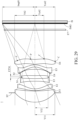
- Fig. 29 shows a schematic view of two inflection points P and two critical points C of the image-side surface of the sixth lens element E6 according to the 1st embodiment of the present disclosure.
- the inflection points P of the image-side surface of the sixth lens element E6 in Fig. 29 are only exemplary.
- Each of the lens elements in various embodiments of the present disclosure can have one or more inflection points.
- the non-axial critical points C of the image-side surface of the sixth lens element E6 in Fig. 29 are only exemplary.
- Each of the lens elements in various embodiments of the present disclosure can have one or more non-axial critical points.
- an f-number of the imaging system lens assembly is Fno
- the following condition can be satisfied: 1.35 ⁇ Fno ⁇ 2.30. Therefore, it is favorable for adjusting the size of the aperture stop so as to obtain a balance between the depth of field and image quality of overall field of view.
- the following condition can also be satisfied: 1.61 ⁇ Fno ⁇ 2.15.
- the following condition can also be satisfied: 1.67 ⁇ Fno ⁇ 2.19.
- the following condition can also be satisfied: 1.67 ⁇ Fno ⁇ 2.05.
- a curvature radius of the object-side surface of the sixth lens element is R11
- a curvature radius of the image-side surface of the sixth lens element is R12
- the following condition can be satisfied: -65.00 ⁇ (R11+R12)/(R11-R12) ⁇ 1.80. Therefore, it is favorable for adjusting the surface shape and refractive power of the sixth lens element so as to maintain the back focal length.
- the following condition can also be satisfied: -58.00 ⁇ (R11+R12)/(R11-R12) ⁇ 0.75.
- a focal length of the first lens element is f1
- a focal length of the third lens element is f3
- the following condition can be satisfied: -0.90 ⁇ f1/f3 ⁇ 2.00. Therefore, it is favorable for balancing the refractive power distribution of the first lens element and the third lens element so as to prevent excessive aberrations generated due to size reduction.
- the following condition can also be satisfied: -0.80 ⁇ f1/f3 ⁇ 1.20.
- the following condition can also be satisfied: -0.65 ⁇ f1/f3 ⁇ 1.10.
- the following condition can be satisfied: -12.00 ⁇ f/R10 ⁇ -0.60. Therefore, it is favorable for adjusting the ratio between the focal length and the curvature radius of the image-side surface of the fifth lens element so as to reduce the manufacturing difficulty of the fifth lens element, thereby increasing manufacturing yield rate. Moreover, the following condition can also be satisfied: -12.00 ⁇ f/R10 ⁇ -1.10. Moreover, the following condition can also be satisfied: -10.00 ⁇ f/R10 ⁇ - 1.20. Moreover, the following condition can also be satisfied: -8.00 ⁇ f/R10 ⁇ -1.40.
- the focal length of the imaging system lens assembly is f
- a curvature radius of the object-side surface of the fifth lens element is R9
- the curvature radius of the image-side surface of the fifth lens element is R10
- the following condition can be satisfied: -25.00 ⁇ f/R9+f/R10 ⁇ -4.70. Therefore, it is favorable for adjusting the ratio between the focal length and the curvature radii of the fifth lens element so as to maintain the curvature strength of the fifth lens element and prevent excessive aberrations generated due to overly large curvature.
- the following condition can also be satisfied: -20.00 ⁇ f/R9+f/R10 ⁇ -6.00.
- the following condition can also be satisfied: -18.00 ⁇ f/R9+f/R10 ⁇ -7.00.
- the following condition can also be satisfied: 0.70 ⁇ (T23+CT3+T34)/(CT4+T45+CT5) ⁇ 3.70. Moreover, the following condition can also be satisfied: 0.71 ⁇ (T23+CT3+T34)/(CT4+T45+CT5) ⁇ 3.50.
- a focal length of the second lens element is f2
- a focal length of the fourth lens element is f4
- the following condition can be satisfied: 0.05 ⁇
- the following condition can also be satisfied: 0.05 ⁇
- the following condition can also be satisfied: 0.06 ⁇
- the following condition can be satisfied: -0.22 ⁇ (R4+R9)/(R4-R9) ⁇ 1.90. Therefore, it is favorable for adjusting the surface shape and the refractive power of the second lens element and the fifth lens element so as to obtain a balance between reducing the total track length and increasing the converging capability. Moreover, the following condition can also be satisfied: -0.20 ⁇ (R4+R9)/(R4-R9) ⁇ 1.50. Moreover, the following condition can also be satisfied: -0.18 ⁇ (R4+R9)/(R4-R9) ⁇ 1.20. Moreover, the following condition can also be satisfied: -0.17 ⁇ (R4+R9)/(R4-R9) ⁇ 0.90.
- Fig. 30 shows a schematic view of SAG41 and SAG42 according to the 1st embodiment of the present disclosure.
- a central thickness of the first lens element is CT1
- a central thickness of the second lens element is CT2
- a central thickness of the sixth lens element is CT6
- the following condition can be satisfied: 4.80 ⁇ (CT1+CT6)/CT2 ⁇ 10.00. Therefore, it is favorable for adjusting the ratio of the central thicknesses of the front side and rear side lens elements to the central thickness of the lens element at the middle part so as to obtain a balance between manufacturing yield rate and the image quality of the central area.
- the following condition can also be satisfied: 5.00 ⁇ (CT1+CT6)/CT2 ⁇ 9.50.
- a maximum image height of the imaging system lens assembly (which can be half of a diagonal length of an effective photosensitive area of an image sensor) is ImgH
- the following condition can be satisfied: 0.10 ⁇ R4/ImgH ⁇ 3.10. Therefore, it is favorable for adjusting the ratio between the curvature radius of the image-side surface of the second lens element and the size of the image surface so as to maintain the surface shape of the second lens element and increase the image surface.
- the following condition can also be satisfied: 0.20 ⁇ R4/ImgH ⁇ 2.70.
- the following condition can also be satisfied: 0.30 ⁇ R4/ImgH ⁇ 2.00.
- Fig. 29 shows a schematic view of ImgH according to the 1st embodiment of the present disclosure.
- the imaging system lens assembly further includes an aperture stop.
- a sum of axial distances between each of all adjacent lens elements of the imaging system lens assembly is ⁇ AT
- an axial distance between the aperture stop and the image-side surface of the sixth lens element is SD
- the following condition can be satisfied: 0.25 ⁇ ⁇ AT/SD ⁇ 0.65. Therefore, it is favorable for obtaining a better space utilization of the imaging system lens assembly so as to prevent interference between lens elements due to an overly small distance between adjacent lens elements and prevent undesirable device portability due to an overly large distance between adjacent lens elements.
- the following condition can also be satisfied: 0.30 ⁇ ⁇ AT/SD ⁇ 0.55.
- the following condition can be satisfied: 13.0 degrees ⁇ HFOV ⁇ 33.0 degrees. Therefore, it is favorable for adjusting the field of view so as to prevent aberrations, such as distortion, generated due to an overly large field of view. Moreover, the following condition can also be satisfied: 14.0 degrees ⁇ HFOV ⁇ 29.0 degrees. Moreover, the following condition can also be satisfied: 15.5 degrees ⁇ HFOV ⁇ 28.0 degrees. Moreover, the following condition can also be satisfied: 17.0 degrees ⁇ HFOV ⁇ 27.0 degrees.
- At least one lens element of the imaging system lens assembly can be made of plastic material. Therefore, it is favorable for reducing manufacturing costs and increasing design flexibility so as to improve image quality and increase mass production.
- a refractive index of the second lens element is N2
- a refractive index of the sixth lens element is N6
- the following condition can be satisfied: 0.95 ⁇ N2/N6 ⁇ 1.25. Therefore, it is favorable for adjusting the ratio between the focal length of the second lens element and the focal length of the sixth lens element so as to ensure sufficient refractive power of the sixth lens element, thereby correcting various aberrations.
- a maximum effective radius of the object-side surface of the first lens element is Y11
- a maximum effective radius of the image-side surface of the sixth lens element is Y62
- the following condition can be satisfied: 0.70 ⁇ Y11/Y62 ⁇ 1.30. Therefore, adjusting the ratio between the optically effective radii of the first lens element and the sixth lens element is favorable for balancing the field of view, size arrangement and image surface area. Moreover, the following condition can also be satisfied: 0.80 ⁇ Y11/Y62 ⁇ 1.15.
- Fig. 29 shows a schematic view of Y11 and Y62 according to the 1st embodiment of the present disclosure.
- the focal length of the first lens element is f1
- a composite focal length of the second lens element, the third lens element and the fourth lens element is f234
- the following condition can be satisfied: -5.00 ⁇ f1/f234 ⁇ -0.03. Therefore, it is favorable for balancing the refractive power distribution at the object side of the imaging system lens assembly so as to correct aberrations.
- the following condition can also be satisfied: -3.00 ⁇ f1/f234 ⁇ -0.10.
- the focal length of the imaging system lens assembly is f
- the maximum image height of the imaging system lens assembly is ImgH
- the following condition can be satisfied: 1.51 ⁇ f/ImgH ⁇ 3.48. Therefore, it is favorable for adjusting the size of the image surface so as to increase light receiving area.
- the following condition can also be satisfied: 1.80 ⁇ f/ImgH ⁇ 3.00.
- the following condition can also be satisfied: 2.05 ⁇ f/ImgH ⁇ 2.95.
- a distance in parallel with the optical axis between a maximum effective radius position of the image-side surface of the third lens element and the maximum effective radius position of the object-side surface of the fourth lens element is ET34
- the axial distance between the third lens element and the fourth lens element is T34
- the following condition can be satisfied: 0.05 ⁇ ET34/T34 ⁇ 1.20. Therefore, it is favorable for adjusting the central thickness and peripheral thickness of an air lens between the third lens element and the fourth lens element so as to obtain a balance between reducing assembly difficulty and reducing stray light in the lens elements.
- Fig. 29 shows a schematic view of ET34 according to the 1st embodiment of the present disclosure.
- an air lens is provided in a space between two adjacent physical lens elements, the air between the two adjacent physical lens elements acts as the transmission medium, and two adjacent lens surfaces of the two adjacent physical lens elements act as refractive interfaces to refract light and correct periphery image.
- a maximum effective radius of the object-side surface of the first lens element is Y11
- a maximum effective radius of the image-side surface of the third lens element is Y32
- the following condition can be satisfied: 1.10 ⁇ Y11/Y32 ⁇ 2.50. Therefore, it is favorable for adjusting the ratio between the effective radii of the first lens element and the third lens element so as to obtain a balance between reducing size, increasing image height and reducing mechanical design difficulty.
- the following condition can also be satisfied: 1.18 ⁇ Y11/Y32 ⁇ 2.10.
- Fig. 29 shows a schematic view of Y11 and Y32 according to the 1st embodiment of the present disclosure.
- a central thickness of the first lens element can be a maximum among central thicknesses of all lens elements of the imaging system lens assembly. Therefore, it is favorable for adjusting the significant light converging capability provided by the first lens element so as to reduce the size of the imaging system lens assembly, thereby achieving compactness.
- the central thickness of the first lens element is CT1
- the central thickness of the fifth lens element is CT5
- the following condition can be satisfied: 1.30 ⁇ CT1/CT5 ⁇ 7.20. Therefore, adjusting the ratio between the central thickness of the first lens element and the central thickness of the fifth lens element is favorable for the first lens element to provide significant light converging capability of the imaging system lens assembly. Moreover, the following condition can also be satisfied: 1.72 ⁇ CT1/CT5 ⁇ 7.00.
- the focal length of the imaging system lens assembly is f
- the focal length of the second lens element is f2
- the following condition can be satisfied: -3.00 ⁇ f/f2 ⁇ - 0.60. Therefore, it is favorable for adjusting the refractive power of the second lens element so as to reduce the effective radius of the middle part of the imaging system lens assembly.
- a refractive index of the first lens element is N1
- the refractive index of the second lens element is N2
- a refractive index of the fifth lens element is N5
- the following condition can be satisfied: 1.90 ⁇ (N1+N2)/N5 ⁇ 2.50. Therefore, it is favorable for balancing material arrangement of lens elements of the imaging system lens assembly so as to optimize light refraction capability of lens elements.
- Fig. 31 shows a schematic view of Drls and Dsr2 according to the 1st embodiment of the present disclosure.
- the following condition can be satisfied: 0.00 ⁇ (T12+T45+T56)/(T23+T34) ⁇ 1.30. Therefore, adjusting the ratio of distances between each of all adjacent lens elements so as to balance the space arrangement of the lens elements is favorable for obtaining a balance between reducing manufacturing errors and reducing temperature change effects. Moreover, the following condition can also be satisfied: 0.03 ⁇ (T12+T45+T56)/(T23+T34) ⁇ 1.20.
- a composite focal length of the first lens element, the second lens element and the third lens element is f123
- a composite focal length of the fourth lens element, the fifth lens element and the sixth lens element is f456
- the following condition can be satisfied: -0.60 ⁇ f123/f456 ⁇ 2.80. Therefore, it is favorable for adjusting the refractive power distribution of the lens elements at the front part and rear part of the imaging system lens assembly so as to maintain the overall stability.
- the following condition can also be satisfied: -0.50 ⁇ f123/f456 ⁇ 2.50.
- the image-side surface of the sixth lens element can have at least one critical point in the off-axis region thereof satisfying the following condition: 0.15 ⁇ Yc62/Y62 ⁇ 0.70. Therefore, adjusting the position of the critical point(s) of the image-side surface of the sixth lens element so as to adjust the incident angle of light on the image surface is favorable for maintaining image quality at various object distances.
- Fig. 29 shows a schematic view of Yc62 and Y62 according to the 1st embodiment of the present disclosure.
- the lens elements of the imaging system lens assembly can be made of either glass or plastic material.
- the refractive power distribution of the imaging system lens assembly may be more flexible, and the influence on imaging caused by external environment temperature change may be reduced.
- the glass lens element can either be made by grinding or molding.
- the manufacturing costs can be effectively reduced.
- surfaces of each lens element can be arranged to be spherical or aspheric. Spherical lens elements are simple in manufacture. Aspheric lens element design allows more control variables for eliminating aberrations thereof and reducing the required number of lens elements, and the total track length of the imaging system lens assembly can therefore be effectively shortened. Additionally, the aspheric surfaces may be formed by plastic injection molding or glass molding.
- a lens surface when a lens surface is aspheric, it means that the lens surface has an aspheric shape throughout its optically effective area, or a portion(s) thereof.
- one or more of the lens elements' material may optionally include an additive which generates light absorption and interference effects and alters the lens elements' transmittance in a specific range of wavelength for a reduction in unwanted stray light or color deviation.
- the additive may optionally filter out light in the wavelength range of 600 nm to 800 nm to reduce excessive red light and/or near infrared light; or may optionally filter out light in the wavelength range of 350 nm to 450 nm to reduce excessive blue light and/or near ultraviolet light from interfering the final image.
- the additive may be homogeneously mixed with a plastic material to be used in manufacturing a mixed-material lens element by injection molding.
- the additive may be coated on the lens surfaces to provide the abovementioned effects.
- each of an object-side surface and an image-side surface has a paraxial region and an off-axis region.
- the paraxial region refers to the region of the surface where light rays travel close to the optical axis
- the off-axis region refers to the region of the surface away from the paraxial region.
- an inflection point is a point on the surface of the lens element at which the surface changes from concave to convex, or vice versa.
- a critical point is a non-axial point of the lens surface where its tangent is perpendicular to the optical axis.
- the image surface of the imaging system lens assembly can be flat or curved, especially a curved surface being concave facing towards the object side of the imaging system lens assembly.
- an image correction unit such as a field flattener
- a field flattener can be optionally disposed between the lens element closest to the image side of the imaging system lens assembly along the optical path and the image surface for correction of aberrations such as field curvature.
- the optical properties of the image correction unit such as curvature, thickness, index of refraction, position and surface shape (convex or concave surface with spherical, aspheric, diffractive or Fresnel types), can be adjusted according to the design of the image capturing unit.
- a preferable image correction unit is, for example, a thin transparent element having a concave object-side surface and a planar image-side surface, and the thin transparent element is disposed near the image surface.
- At least one light-folding element such as a prism or a mirror, can be optionally disposed between an imaged object and the image surface on the imaging optical path, such that the imaging system lens assembly can be more flexible in space arrangement, and therefore the dimensions of an electronic device is not restricted by the total track length of the imaging system lens assembly.
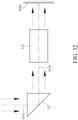
- Fig. 32 and Fig. 33 show a schematic view of a configuration of a light-folding element in an imaging system lens assembly according to one embodiment of the present disclosure
- Fig. 33 shows a schematic view of another configuration of a light-folding element in an imaging system lens assembly according to one embodiment of the present disclosure.
- the imaging system lens assembly can have, in order from an imaged object (not shown in the figures) to an image surface IMG along an optical path, a first optical axis OA1, a light-folding element LF and a second optical axis OA2.
- the light-folding element LF can be disposed between the imaged object and a lens group LG of the imaging system lens assembly as shown in Fig. 32 or disposed between a lens group LG of the imaging system lens assembly and the image surface IMG as shown in Fig. 33 .
- Fig. 34 shows a schematic view of a configuration of two light-folding elements in an imaging system lens assembly according to one embodiment of the present disclosure. In Fig.
- the imaging system lens assembly can have, in order from an imaged object (not shown in the figure) to an image surface IMG along an optical path, a first optical axis OA1, a first light-folding element LF1, a second optical axis OA2, a second light-folding element LF2 and a third optical axis OA3.
- the first light-folding element LF1 is disposed between the imaged object and a lens group LG of the imaging system lens assembly
- the second light-folding element LF2 is disposed between the lens group LG of the imaging system lens assembly and the image surface IMG
- the travelling direction of light on the first optical axis OA1 can be the same direction as the travelling direction of light on the third optical axis OA3 as shown in Fig. 34 .
- the imaging system lens assembly can be optionally provided with three or more light-folding elements, and the present disclosure is not limited to the type, amount and position of the light-folding elements of the embodiments disclosed in the aforementioned figures.
- the imaging system lens assembly can include at least one stop, such as an aperture stop, a glare stop or a field stop. Said glare stop or said field stop is set for eliminating the stray light and thereby improving image quality thereof.
- an aperture stop can be configured as a front stop or a middle stop.
- a front stop disposed between an imaged object and the first lens element can provide a longer distance between an exit pupil of the imaging system lens assembly and the image surface to produce a telecentric effect, and thereby improves the image-sensing efficiency of an image sensor (for example, CCD or CMOS).
- a middle stop disposed between the first lens element and the image surface is favorable for enlarging the viewing angle of the imaging system lens assembly and thereby provides a wider field of view for the same.
- the imaging system lens assembly can include an aperture control unit.
- the aperture control unit may be a mechanical component or a light modulator, which can control the size and shape of the aperture through electricity or electrical signals.
- the mechanical component can include a movable member, such as a blade assembly or a light shielding sheet.
- the light modulator can include a shielding element, such as a filter, an electrochromic material or a liquid-crystal layer.
- the aperture control unit controls the amount of incident light or exposure time to enhance the capability of image quality adjustment.
- the aperture control unit can be the aperture stop of the present disclosure, which changes the f-number to obtain different image effects, such as the depth of field or lens speed.
- the imaging system lens assembly can include one or more optical elements for limiting the form of light passing through the imaging system lens assembly.
- Each optical element can be, but not limited to, a filter, a polarizer, etc., and each optical element can be, but not limited to, a single-piece element, a composite component, a thin film, etc.
- the optical element can be located at the front side or the rear side of the imaging system lens assembly or between any two adjacent lens elements so as to allow light in a specific form to pass through, thereby meeting application requirements.
- Fig. 1 is a schematic view of an image capturing unit according to the 1st embodiment of the present disclosure.
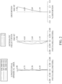
- Fig. 2 shows, in order from left to right, spherical aberration curves, astigmatic field curves and a distortion curve of the image capturing unit according to the 1st embodiment.
- the image capturing unit 1 includes the imaging system lens assembly (its reference numeral is omitted) of the present disclosure and an image sensor IS.
- the imaging system lens assembly includes, in order from an object side to an image side along an optical axis, an aperture stop ST, a first lens element E1, a second lens element E2, a third lens element E3, a stop S1, a fourth lens element E4, a stop S2, a fifth lens element E5, a sixth lens element E6, a filter E7 and an image surface IMG.
- the imaging system lens assembly includes six lens elements (E1, E2, E3, E4, E5 and E6) with no additional lens element disposed between each of the adjacent six lens elements.
- the first lens element E1 with positive refractive power has an object-side surface being convex in a paraxial region thereof and an image-side surface being concave in a paraxial region thereof.
- the first lens element E1 is made of glass material and has the object-side surface and the image-side surface being both spherical.
- the second lens element E2 with negative refractive power has an object-side surface being convex in a paraxial region thereof and an image-side surface being concave in a paraxial region thereof.
- the second lens element E2 is made of plastic material and has the object-side surface and the image-side surface being both aspheric.
- the third lens element E3 with negative refractive power has an object-side surface being concave in a paraxial region thereof and an image-side surface being concave in a paraxial region thereof.
- the third lens element E3 is made of plastic material and has the object-side surface and the image-side surface being both aspheric.
- the fourth lens element E4 with positive refractive power has an object-side surface being convex in a paraxial region thereof and an image-side surface being convex in a paraxial region thereof.
- the fourth lens element E4 is made of plastic material and has the object-side surface and the image-side surface being both aspheric.
- the fifth lens element E5 with negative refractive power has an object-side surface being concave in a paraxial region thereof and an image-side surface being convex in a paraxial region thereof.
- the fifth lens element E5 is made of plastic material and has the object-side surface and the image-side surface being both aspheric.
- the sixth lens element E6 with positive refractive power has an object-side surface being convex in a paraxial region thereof and an image-side surface being concave in a paraxial region thereof.
- the sixth lens element E6 is made of plastic material and has the object-side surface and the image-side surface being both aspheric.
- the image-side surface of the sixth lens element E6 has two inflection points.
- the image-side surface of the sixth lens element E6 has two critical points in an off-axis region thereof.
- the filter E7 is made of glass material and located between the sixth lens element E6 and the image surface IMG, and will not affect the focal length of the imaging system lens assembly.
- the image sensor IS is disposed on or near the image surface IMG of the imaging system lens assembly.
- f 12.22 millimeters (mm)
- Fno 1.85
- HFOV 23.2 degrees (deg.).
- a curvature radius of the object-side surface of the fifth lens element E5 is R9
- the curvature radius of the image-side surface of the fifth lens element E5 is R10
- CT1/CT5 5.07.
- an axial distance between the first lens element E1 and the second lens element E2 is T12
- an axial distance between the second lens element E2 and the third lens element E3 is T23
- an axial distance between the third lens element E3 and the fourth lens element E4 is T34
- an axial distance between the fourth lens element E4 and the fifth lens element E5 is T45
- an axial distance between the fifth lens element E5 and the sixth lens element E6 is T56
- ⁇ AT is the sum of the axial distances between the first lens element E1 and the second lens element E2, the second lens element E2 and the third lens element E3, the third lens element E3 and the fourth lens element E4, the fourth lens element E4 and the fifth lens element E5, and the fifth lens element E5 and the sixth lens element E6.
- a vertical distance between a critical point on the image-side surface of the sixth lens element E6 and the optical axis is Yc62, and the maximum effective radius of the image-side surface of the sixth lens element E6 is Y62
- ET34/T34 0.58.
- Drls an axial displacement from the object-side surface of the first lens element E1 to the aperture stop ST
- Dsr2 an axial displacement from the aperture stop ST to the image-side surface of the first lens element E1
- Dr1s/Dsr2 5.37.
- the directions of Drls and Dsr2 are facing towards the image side of the imaging system lens assembly, so the values of Drls and Dsr2 are positive.
- An effective radius of the stop S1 (Surface 8) is 2.188 mm.
- An effective radius of the stop S2 (Surface 11) is 2.456 mm.
- TABLE 1B Aspheric Coefficients Surface # 4 5 6 7 k -4.78884E-01 -5.90960E-02 -7.48491E+01 3.64632E+01
- A4 -1.71443836E-02 -2.16337920E-02 -1.13990894E-02 -2.04269101E-02
- A10 6.43204378E-04 -3.34672974E-04 1.13308403E-04 -2.55073191E-03
- A12 -3.5994
- Table 1A the curvature radius, the thickness and the focal length are shown in millimeters (mm).
- Surface numbers 0-18 represent the surfaces sequentially arranged from the object side to the image side along the optical axis.
- Table 1B k represents the conic coefficient of the equation of the aspheric surface profiles.
- A4-A26 represent the aspheric coefficients ranging from the 4th order to the 26th order.
- Fig. 3 is a schematic view of an image capturing unit according to the 2nd embodiment of the present disclosure.
- Fig. 4 shows, in order from left to right, spherical aberration curves, astigmatic field curves and a distortion curve of the image capturing unit according to the 2nd embodiment.
- the image capturing unit 2 includes the imaging system lens assembly (its reference numeral is omitted) of the present disclosure and an image sensor IS.
- the imaging system lens assembly includes, in order from an object side to an image side along an optical axis, an aperture stop ST, a first lens element E1, a second lens element E2, a third lens element E3, a stop S1, a fourth lens element E4, a stop S2, a fifth lens element E5, a sixth lens element E6, a stop S3, a filter E7 and an image surface IMG.
- the imaging system lens assembly includes six lens elements (E1, E2, E3, E4, E5 and E6) with no additional lens element disposed between each of the adjacent six lens elements.
- the first lens element E1 with positive refractive power has an object-side surface being convex in a paraxial region thereof and an image-side surface being convex in a paraxial region thereof.
- the first lens element E1 is made of plastic material and has the object-side surface and the image-side surface being both aspheric.
- the second lens element E2 with negative refractive power has an object-side surface being convex in a paraxial region thereof and an image-side surface being concave in a paraxial region thereof.
- the second lens element E2 is made of plastic material and has the object-side surface and the image-side surface being both aspheric.
- the third lens element E3 with positive refractive power has an object-side surface being convex in a paraxial region thereof and an image-side surface being concave in a paraxial region thereof.
- the third lens element E3 is made of plastic material and has the object-side surface and the image-side surface being both aspheric.
- the fourth lens element E4 with positive refractive power has an object-side surface being concave in a paraxial region thereof and an image-side surface being convex in a paraxial region thereof.
- the fourth lens element E4 is made of plastic material and has the object-side surface and the image-side surface being both aspheric.
- the fifth lens element E5 with negative refractive power has an object-side surface being concave in a paraxial region thereof and an image-side surface being convex in a paraxial region thereof.
- the fifth lens element E5 is made of plastic material and has the object-side surface and the image-side surface being both aspheric.
- the sixth lens element E6 with positive refractive power has an object-side surface being convex in a paraxial region thereof and an image-side surface being concave in a paraxial region thereof.
- the sixth lens element E6 is made of plastic material and has the object-side surface and the image-side surface being both aspheric.
- the image-side surface of the sixth lens element E6 has two inflection points.
- the image-side surface of the sixth lens element E6 has one critical point in an off-axis region thereof.
- the filter E7 is made of glass material and located between the sixth lens element E6 and the image surface IMG, and will not affect the focal length of the imaging system lens assembly.
- the image sensor IS is disposed on or near the image surface IMG of the imaging system lens assembly.
- An effective radius of the stop S1 (Surface 8) is 2.161 mm.
- An effective radius of the stop S2 (Surface 11) is 2.192 mm.
- An effective radius of the stop S3 (Surface 16) is 3.523 mm.
- Fig. 5 is a schematic view of an image capturing unit according to the 3rd embodiment of the present disclosure.
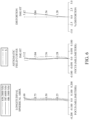
- Fig. 6 shows, in order from left to right, spherical aberration curves, astigmatic field curves and a distortion curve of the image capturing unit according to the 3rd embodiment.
- the image capturing unit 3 includes the imaging system lens assembly (its reference numeral is omitted) of the present disclosure and an image sensor IS.
- the imaging system lens assembly includes, in order from an object side to an image side along an optical axis, an aperture stop ST, a first lens element E1, a second lens element E2, a third lens element E3, a stop S1, a fourth lens element E4, a stop S2, a fifth lens element E5, a sixth lens element E6, a filter E7 and an image surface IMG.
- the imaging system lens assembly includes six lens elements (E1, E2, E3, E4, E5 and E6) with no additional lens element disposed between each of the adjacent six lens elements.
- the first lens element E1 with positive refractive power has an object-side surface being convex in a paraxial region thereof and an image-side surface being concave in a paraxial region thereof.
- the first lens element E1 is made of plastic material and has the object-side surface and the image-side surface being both aspheric.
- the second lens element E2 with negative refractive power has an object-side surface being convex in a paraxial region thereof and an image-side surface being concave in a paraxial region thereof.
- the second lens element E2 is made of plastic material and has the object-side surface and the image-side surface being both aspheric.
- the third lens element E3 with positive refractive power has an object-side surface being convex in a paraxial region thereof and an image-side surface being concave in a paraxial region thereof.
- the third lens element E3 is made of plastic material and has the object-side surface and the image-side surface being both aspheric.
- the fourth lens element E4 with positive refractive power has an object-side surface being convex in a paraxial region thereof and an image-side surface being concave in a paraxial region thereof.
- the fourth lens element E4 is made of plastic material and has the object-side surface and the image-side surface being both aspheric.
- the fifth lens element E5 with negative refractive power has an object-side surface being concave in a paraxial region thereof and an image-side surface being convex in a paraxial region thereof.
- the fifth lens element E5 is made of plastic material and has the object-side surface and the image-side surface being both aspheric.
- the sixth lens element E6 with positive refractive power has an object-side surface being convex in a paraxial region thereof and an image-side surface being concave in a paraxial region thereof.
- the sixth lens element E6 is made of plastic material and has the object-side surface and the image-side surface being both aspheric.
- the image-side surface of the sixth lens element E6 has two inflection points.
- the image-side surface of the sixth lens element E6 has one critical point in an off-axis region thereof.
- the filter E7 is made of glass material and located between the sixth lens element E6 and the image surface IMG, and will not affect the focal length of the imaging system lens assembly.
- the image sensor IS is disposed on or near the image surface IMG of the imaging system lens assembly.
- An effective radius of the stop S1 (Surface 8) is 2.130 mm.
- An effective radius of the stop S2 (Surface 11) is 2.200 mm.
- the equation of the aspheric surface profiles of the aforementioned lens elements is the same as the equation of the 1st embodiment. Also, the definitions of these parameters shown in Table 3C below are the same as those stated in the 1st embodiment with corresponding values for the 3rd embodiment, so an explanation in this regard will not be provided again.
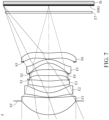
- Fig. 7 is a schematic view of an image capturing unit according to the 4th embodiment of the present disclosure.
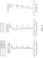
- Fig. 8 shows, in order from left to right, spherical aberration curves, astigmatic field curves and a distortion curve of the image capturing unit according to the 4th embodiment.
- the image capturing unit 4 includes the imaging system lens assembly (its reference numeral is omitted) of the present disclosure and an image sensor IS.
- the imaging system lens assembly includes, in order from an object side to an image side along an optical axis, an aperture stop ST, a first lens element E1, a second lens element E2, a third lens element E3, a stop S1, a fourth lens element E4, a stop S2, a fifth lens element E5, a stop S3, a sixth lens element E6, a filter E7 and an image surface IMG.
- the imaging system lens assembly includes six lens elements (E1, E2, E3, E4, E5 and E6) with no additional lens element disposed between each of the adjacent six lens elements.
- the first lens element E1 with positive refractive power has an object-side surface being convex in a paraxial region thereof and an image-side surface being concave in a paraxial region thereof.
- the first lens element E1 is made of glass material and has the object-side surface and the image-side surface being both aspheric.
- the second lens element E2 with negative refractive power has an object-side surface being convex in a paraxial region thereof and an image-side surface being concave in a paraxial region thereof.
- the second lens element E2 is made of plastic material and has the object-side surface and the image-side surface being both aspheric.
- the third lens element E3 with positive refractive power has an object-side surface being convex in a paraxial region thereof and an image-side surface being concave in a paraxial region thereof.
- the third lens element E3 is made of plastic material and has the object-side surface and the image-side surface being both aspheric.
- the fourth lens element E4 with positive refractive power has an object-side surface being convex in a paraxial region thereof and an image-side surface being convex in a paraxial region thereof.
- the fourth lens element E4 is made of plastic material and has the object-side surface and the image-side surface being both aspheric.
- the fifth lens element E5 with negative refractive power has an object-side surface being concave in a paraxial region thereof and an image-side surface being convex in a paraxial region thereof.
- the fifth lens element E5 is made of plastic material and has the object-side surface and the image-side surface being both aspheric.
- the sixth lens element E6 with positive refractive power has an object-side surface being convex in a paraxial region thereof and an image-side surface being concave in a paraxial region thereof.
- the sixth lens element E6 is made of plastic material and has the object-side surface and the image-side surface being both aspheric.
- the image-side surface of the sixth lens element E6 has two inflection points.
- the image-side surface of the sixth lens element E6 has one critical point in an off-axis region thereof.
- the filter E7 is made of glass material and located between the sixth lens element E6 and the image surface IMG, and will not affect the focal length of the imaging system lens assembly.
- the image sensor IS is disposed on or near the image surface IMG of the imaging system lens assembly.
- An effective radius of the stop S1 (Surface 8) is 2.254 mm.
- An effective radius of the stop S2 (Surface 11) is 2.220 mm.
- An effective radius of the stop S3 (Surface 14) is 2.899 mm.
- the equation of the aspheric surface profiles of the aforementioned lens elements is the same as the equation of the 1st embodiment. Also, the definitions of these parameters shown in Table 4C below are the same as those stated in the 1st embodiment with corresponding values for the 4th embodiment, so an explanation in this regard will not be provided again.
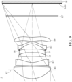
- Fig. 9 is a schematic view of an image capturing unit according to the 5th embodiment of the present disclosure.
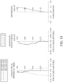
- Fig. 10 shows, in order from left to right, spherical aberration curves, astigmatic field curves and a distortion curve of the image capturing unit according to the 5th embodiment.
- the image capturing unit 5 includes the imaging system lens assembly (its reference numeral is omitted) of the present disclosure and an image sensor IS.
- the imaging system lens assembly includes, in order from an object side to an image side along an optical axis, an aperture stop ST, a first lens element E1, a second lens element E2, a third lens element E3, a fourth lens element E4, a stop S1, a fifth lens element E5, a sixth lens element E6, a filter E7 and an image surface IMG.
- the imaging system lens assembly includes six lens elements (E1, E2, E3, E4, E5 and E6) with no additional lens element disposed between each of the adjacent six lens elements.
- the first lens element E1 with positive refractive power has an object-side surface being convex in a paraxial region thereof and an image-side surface being convex in a paraxial region thereof.
- the first lens element E1 is made of plastic material and has the object-side surface and the image-side surface being both aspheric.
- the second lens element E2 with negative refractive power has an object-side surface being convex in a paraxial region thereof and an image-side surface being concave in a paraxial region thereof.
- the second lens element E2 is made of plastic material and has the object-side surface and the image-side surface being both aspheric.
- the third lens element E3 with positive refractive power has an object-side surface being convex in a paraxial region thereof and an image-side surface being convex in a paraxial region thereof.
- the third lens element E3 is made of plastic material and has the object-side surface and the image-side surface being both aspheric.
- the fourth lens element E4 with negative refractive power has an object-side surface being concave in a paraxial region thereof and an image-side surface being concave in a paraxial region thereof.
- the fourth lens element E4 is made of plastic material and has the object-side surface and the image-side surface being both aspheric.
- the image-side surface of the third lens element E3 and the object-side surface of the fourth lens element E4 are cemented to each other.
- the fifth lens element E5 with negative refractive power has an object-side surface being concave in a paraxial region thereof and an image-side surface being convex in a paraxial region thereof.
- the fifth lens element E5 is made of plastic material and has the object-side surface and the image-side surface being both aspheric.
- the sixth lens element E6 with positive refractive power has an object-side surface being convex in a paraxial region thereof and an image-side surface being concave in a paraxial region thereof.
- the sixth lens element E6 is made of plastic material and has the object-side surface and the image-side surface being both aspheric.
- the image-side surface of the sixth lens element E6 has one inflection point.
- the image-side surface of the sixth lens element E6 has one critical point in an off-axis region thereof.
- the filter E7 is made of glass material and located between the sixth lens element E6 and the image surface IMG, and will not affect the focal length of the imaging system lens assembly.
- the image sensor IS is disposed on or near the image surface IMG of the imaging system lens assembly.
- An effective radius of the stop S1 (Surface 10) is 2.217 mm.
- the equation of the aspheric surface profiles of the aforementioned lens elements is the same as the equation of the 1st embodiment. Also, the definitions of these parameters shown in Table 5C below are the same as those stated in the 1st embodiment with corresponding values for the 5th embodiment, so an explanation in this regard will not be provided again.
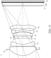
- Fig. 11 is a schematic view of an image capturing unit according to the 6th embodiment of the present disclosure.
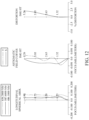
- Fig. 12 shows, in order from left to right, spherical aberration curves, astigmatic field curves and a distortion curve of the image capturing unit according to the 6th embodiment.
- the image capturing unit 6 includes the imaging system lens assembly (its reference numeral is omitted) of the present disclosure and an image sensor IS.
- the imaging system lens assembly includes, in order from an object side to an image side along an optical axis, an aperture stop ST, a first lens element E1, a second lens element E2, a third lens element E3, a stop S1, a fourth lens element E4, a fifth lens element E5, a sixth lens element E6, a filter E7 and an image surface IMG.
- the imaging system lens assembly includes six lens elements (E1, E2, E3, E4, E5 and E6) with no additional lens element disposed between each of the adjacent six lens elements.
- the first lens element E1 with positive refractive power has an object-side surface being convex in a paraxial region thereof and an image-side surface being convex in a paraxial region thereof.
- the first lens element E1 is made of glass material and has the object-side surface and the image-side surface being both aspheric.
- the second lens element E2 with negative refractive power has an object-side surface being convex in a paraxial region thereof and an image-side surface being concave in a paraxial region thereof.
- the second lens element E2 is made of plastic material and has the object-side surface and the image-side surface being both aspheric.
- the third lens element E3 with positive refractive power has an object-side surface being concave in a paraxial region thereof and an image-side surface being convex in a paraxial region thereof.
- the third lens element E3 is made of plastic material and has the object-side surface and the image-side surface being both aspheric.
- the fourth lens element E4 with positive refractive power has an object-side surface being convex in a paraxial region thereof and an image-side surface being convex in a paraxial region thereof.
- the fourth lens element E4 is made of plastic material and has the object-side surface and the image-side surface being both aspheric.
- the fifth lens element E5 with negative refractive power has an object-side surface being concave in a paraxial region thereof and an image-side surface being convex in a paraxial region thereof.
- the fifth lens element E5 is made of plastic material and has the object-side surface and the image-side surface being both aspheric.
- the sixth lens element E6 with positive refractive power has an object-side surface being convex in a paraxial region thereof and an image-side surface being concave in a paraxial region thereof.
- the sixth lens element E6 is made of plastic material and has the object-side surface and the image-side surface being both aspheric.
- the image-side surface of the sixth lens element E6 has two inflection points.
- the image-side surface of the sixth lens element E6 has one critical point in an off-axis region thereof.
- the filter E7 is made of glass material and located between the sixth lens element E6 and the image surface IMG, and will not affect the focal length of the imaging system lens assembly.
- the image sensor IS is disposed on or near the image surface IMG of the imaging system lens assembly.
- An effective radius of the stop S1 (Surface 8) is 2.116 mm.
- the equation of the aspheric surface profiles of the aforementioned lens elements is the same as the equation of the 1st embodiment. Also, the definitions of these parameters shown in Table 6C below are the same as those stated in the 1st embodiment with corresponding values for the 6th embodiment, so an explanation in this regard will not be provided again.
- Fig. 13 is a schematic view of an image capturing unit according to the 7th embodiment of the present disclosure.
- Fig. 14 shows, in order from left to right, spherical aberration curves, astigmatic field curves and a distortion curve of the image capturing unit according to the 7th embodiment.
- the image capturing unit 7 includes the imaging system lens assembly (its reference numeral is omitted) of the present disclosure and an image sensor IS.
- the imaging system lens assembly includes, in order from an object side to an image side along an optical axis, an aperture stop ST, a first lens element E1, a second lens element E2, a third lens element E3, a fourth lens element E4, a stop S1, a fifth lens element E5, a sixth lens element E6, a filter E7 and an image surface IMG.
- the imaging system lens assembly includes six lens elements (E1, E2, E3, E4, E5 and E6) with no additional lens element disposed between each of the adjacent six lens elements.
- the first lens element E1 with positive refractive power has an object-side surface being convex in a paraxial region thereof and an image-side surface being convex in a paraxial region thereof.
- the first lens element E1 is made of glass material and has the object-side surface and the image-side surface being both aspheric.
- the second lens element E2 with negative refractive power has an object-side surface being concave in a paraxial region thereof and an image-side surface being concave in a paraxial region thereof.
- the second lens element E2 is made of plastic material and has the object-side surface and the image-side surface being both aspheric.
- the third lens element E3 with negative refractive power has an object-side surface being convex in a paraxial region thereof and an image-side surface being concave in a paraxial region thereof.
- the third lens element E3 is made of plastic material and has the object-side surface and the image-side surface being both aspheric.
- the fourth lens element E4 with positive refractive power has an object-side surface being convex in a paraxial region thereof and an image-side surface being convex in a paraxial region thereof.
- the fourth lens element E4 is made of plastic material and has the object-side surface and the image-side surface being both aspheric.
- the fifth lens element E5 with negative refractive power has an object-side surface being concave in a paraxial region thereof and an image-side surface being convex in a paraxial region thereof.
- the fifth lens element E5 is made of plastic material and has the object-side surface and the image-side surface being both aspheric.
- the sixth lens element E6 with positive refractive power has an object-side surface being convex in a paraxial region thereof and an image-side surface being concave in a paraxial region thereof.
- the sixth lens element E6 is made of plastic material and has the object-side surface and the image-side surface being both aspheric.
- the image-side surface of the sixth lens element E6 has two inflection points.
- the image-side surface of the sixth lens element E6 has one critical point in an off-axis region thereof.
- the filter E7 is made of glass material and located between the sixth lens element E6 and the image surface IMG, and will not affect the focal length of the imaging system lens assembly.
- the image sensor IS is disposed on or near the image surface IMG of the imaging system lens assembly.
- An effective radius of the stop S1 (Surface 10) is 2.240 mm.
- the equation of the aspheric surface profiles of the aforementioned lens elements is the same as the equation of the 1st embodiment. Also, the definitions of these parameters shown in Table 7C below are the same as those stated in the 1st embodiment with corresponding values for the 7th embodiment, so an explanation in this regard will not be provided again.
- Fig. 15 is a schematic view of an image capturing unit according to the 8th embodiment of the present disclosure.
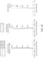
- Fig. 16 shows, in order from left to right, spherical aberration curves, astigmatic field curves and a distortion curve of the image capturing unit according to the 8th embodiment.
- the image capturing unit 8 includes the imaging system lens assembly (its reference numeral is omitted) of the present disclosure and an image sensor IS.
- the imaging system lens assembly includes, in order from an object side to an image side along an optical axis, an aperture stop ST, a first lens element E1, a second lens element E2, a third lens element E3, a stop S1, a fourth lens element E4, a fifth lens element E5, a stop S2, a sixth lens element E6, a filter E7 and an image surface IMG.
- the imaging system lens assembly includes six lens elements (E1, E2, E3, E4, E5 and E6) with no additional lens element disposed between each of the adjacent six lens elements.
- the first lens element E1 with positive refractive power has an object-side surface being convex in a paraxial region thereof and an image-side surface being concave in a paraxial region thereof.
- the first lens element E1 is made of plastic material and has the object-side surface and the image-side surface being both aspheric.
- the second lens element E2 with negative refractive power has an object-side surface being convex in a paraxial region thereof and an image-side surface being concave in a paraxial region thereof.
- the second lens element E2 is made of plastic material and has the object-side surface and the image-side surface being both aspheric.
- the third lens element E3 with positive refractive power has an object-side surface being convex in a paraxial region thereof and an image-side surface being concave in a paraxial region thereof.
- the third lens element E3 is made of plastic material and has the object-side surface and the image-side surface being both aspheric.
- the fourth lens element E4 with negative refractive power has an object-side surface being concave in a paraxial region thereof and an image-side surface being convex in a paraxial region thereof.
- the fourth lens element E4 is made of plastic material and has the object-side surface and the image-side surface being both aspheric.
- the fifth lens element E5 with positive refractive power has an object-side surface being concave in a paraxial region thereof and an image-side surface being convex in a paraxial region thereof.
- the fifth lens element E5 is made of plastic material and has the object-side surface and the image-side surface being both aspheric.
- the sixth lens element E6 with positive refractive power has an object-side surface being convex in a paraxial region thereof and an image-side surface being concave in a paraxial region thereof.
- the sixth lens element E6 is made of plastic material and has the object-side surface and the image-side surface being both aspheric.
- the image-side surface of the sixth lens element E6 has two inflection points.
- the image-side surface of the sixth lens element E6 has one critical point in an off-axis region thereof.
- the filter E7 is made of glass material and located between the sixth lens element E6 and the image surface IMG, and will not affect the focal length of the imaging system lens assembly.
- the image sensor IS is disposed on or near the image surface IMG of the imaging system lens assembly.
- An effective radius of the stop S1 (Surface 8) is 2.072 mm.
- An effective radius of the stop S2 (Surface 13) is 3.311 mm.
- the equation of the aspheric surface profiles of the aforementioned lens elements is the same as the equation of the 1st embodiment. Also, the definitions of these parameters shown in Table 8C below are the same as those stated in the 1st embodiment with corresponding values for the 8th embodiment, so an explanation in this regard will not be provided again.
- Fig. 17 is a schematic view of an image capturing unit according to the 9th embodiment of the present disclosure.
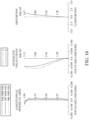
- Fig. 18 shows, in order from left to right, spherical aberration curves, astigmatic field curves and a distortion curve of the image capturing unit according to the 9th embodiment.
- the image capturing unit 9 includes the imaging system lens assembly (its reference numeral is omitted) of the present disclosure and an image sensor IS.
- the imaging system lens assembly includes, in order from an object side to an image side along an optical axis, an aperture stop ST, a first lens element E1, a second lens element E2, a third lens element E3, a stop S1, a fourth lens element E4, a stop S2, a fifth lens element E5, a sixth lens element E6, a filter E7 and an image surface IMG.
- the imaging system lens assembly includes six lens elements (E1, E2, E3, E4, E5 and E6) with no additional lens element disposed between each of the adjacent six lens elements.
- the first lens element E1 with positive refractive power has an object-side surface being convex in a paraxial region thereof and an image-side surface being concave in a paraxial region thereof.
- the first lens element E1 is made of glass material and has the object-side surface and the image-side surface being both aspheric.
- the second lens element E2 with negative refractive power has an object-side surface being convex in a paraxial region thereof and an image-side surface being concave in a paraxial region thereof.
- the second lens element E2 is made of plastic material and has the object-side surface and the image-side surface being both aspheric.
- the third lens element E3 with positive refractive power has an object-side surface being convex in a paraxial region thereof and an image-side surface being concave in a paraxial region thereof.
- the third lens element E3 is made of plastic material and has the object-side surface and the image-side surface being both aspheric.
- the fourth lens element E4 with negative refractive power has an object-side surface being concave in a paraxial region thereof and an image-side surface being convex in a paraxial region thereof.
- the fourth lens element E4 is made of plastic material and has the object-side surface and the image-side surface being both aspheric.
- the fifth lens element E5 with positive refractive power has an object-side surface being concave in a paraxial region thereof and an image-side surface being convex in a paraxial region thereof.
- the fifth lens element E5 is made of plastic material and has the object-side surface and the image-side surface being both aspheric.
- the sixth lens element E6 with negative refractive power has an object-side surface being concave in a paraxial region thereof and an image-side surface being concave in a paraxial region thereof.
- the sixth lens element E6 is made of plastic material and has the object-side surface and the image-side surface being both aspheric.
- the image-side surface of the sixth lens element E6 has two inflection points.
- the image-side surface of the sixth lens element E6 has one critical point in an off-axis region thereof.
- the filter E7 is made of glass material and located between the sixth lens element E6 and the image surface IMG, and will not affect the focal length of the imaging system lens assembly.
- the image sensor IS is disposed on or near the image surface IMG of the imaging system lens assembly.
- An effective radius of the stop S1 (Surface 8) is 1.866 mm.
- An effective radius of the stop S2 (Surface 11) is 2.240 mm.
- the equation of the aspheric surface profiles of the aforementioned lens elements is the same as the equation of the 1st embodiment. Also, the definitions of these parameters shown in Table 9C below are the same as those stated in the 1st embodiment with corresponding values for the 9th embodiment, so an explanation in this regard will not be provided again.
- Fig. 19 is a schematic view of an image capturing unit according to the 10th embodiment of the present disclosure.
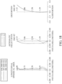
- Fig. 20 shows, in order from left to right, spherical aberration curves, astigmatic field curves and a distortion curve of the image capturing unit according to the 10th embodiment.
- the image capturing unit 10 includes the imaging system lens assembly (its reference numeral is omitted) of the present disclosure and an image sensor IS.
- the imaging system lens assembly includes, in order from an object side to an image side along an optical axis, a first lens element E1, a second lens element E2, an aperture stop ST, a third lens element E3, a fourth lens element E4, a stop S1, a fifth lens element E5, a sixth lens element E6, a filter E7 and an image surface IMG.
- the imaging system lens assembly includes six lens elements (E1, E2, E3, E4, E5 and E6) with no additional lens element disposed between each of the adjacent six lens elements.
- the first lens element E1 with positive refractive power has an object-side surface being convex in a paraxial region thereof and an image-side surface being concave in a paraxial region thereof.
- the first lens element E1 is made of plastic material and has the object-side surface and the image-side surface being both aspheric.
- the second lens element E2 with negative refractive power has an object-side surface being convex in a paraxial region thereof and an image-side surface being concave in a paraxial region thereof.
- the second lens element E2 is made of plastic material and has the object-side surface and the image-side surface being both aspheric.
- the third lens element E3 with positive refractive power has an object-side surface being convex in a paraxial region thereof and an image-side surface being concave in a paraxial region thereof.
- the third lens element E3 is made of plastic material and has the object-side surface and the image-side surface being both aspheric.
- the fourth lens element E4 with positive refractive power has an object-side surface being convex in a paraxial region thereof and an image-side surface being concave in a paraxial region thereof.
- the fourth lens element E4 is made of plastic material and has the object-side surface and the image-side surface being both aspheric.
- the fifth lens element E5 with negative refractive power has an object-side surface being concave in a paraxial region thereof and an image-side surface being convex in a paraxial region thereof.
- the fifth lens element E5 is made of plastic material and has the object-side surface and the image-side surface being both aspheric.
- the sixth lens element E6 with positive refractive power has an object-side surface being convex in a paraxial region thereof and an image-side surface being concave in a paraxial region thereof.
- the sixth lens element E6 is made of plastic material and has the object-side surface and the image-side surface being both aspheric.
- the image-side surface of the sixth lens element E6 has two inflection points.
- the image-side surface of the sixth lens element E6 has one critical point in an off-axis region thereof.
- the filter E7 is made of glass material and located between the sixth lens element E6 and the image surface IMG, and will not affect the focal length of the imaging system lens assembly.
- the image sensor IS is disposed on or near the image surface IMG of the imaging system lens assembly.
- An effective radius of the stop S1 (Surface 10) is 2.210 mm.
- the equation of the aspheric surface profiles of the aforementioned lens elements is the same as the equation of the 1st embodiment. Also, the definitions of these parameters shown in Table 10C below are the same as those stated in the 1st embodiment with corresponding values for the 10th embodiment, so an explanation in this regard will not be provided again.
- Fig. 21 is a perspective view of an image capturing unit according to the 11th embodiment of the present disclosure.
- an image capturing unit 100 is a camera module including a lens unit 101, a driving device 102, an image sensor 103 and an image stabilizer 104.
- the lens unit 101 includes the imaging system lens assembly as disclosed in the 1st embodiment, a barrel and a holder member (their reference numerals are omitted) for holding the imaging system lens assembly.
- the lens unit 101 may alternatively be provided with the imaging system lens assembly disclosed in other embodiments of the present disclosure, and the present disclosure is not limited thereto.
- the imaging light converges in the lens unit 101 of the image capturing unit 100 to generate an image with the driving device 102 utilized for image focusing on the image sensor 103, and the generated image is then digitally transmitted to other electronic component for further processing.
- the driving device 102 can have auto focusing functionality, and different driving configurations can be obtained through the usages of voice coil motors (VCM), micro electro-mechanical systems (MEMS), piezoelectric systems or shape memory alloy materials.
- VCM voice coil motors
- MEMS micro electro-mechanical systems
- the driving device 102 is favorable for obtaining a better imaging position of the lens unit 101, so that a clear image of the imaged object can be captured by the lens unit 101 with different object distances.
- the image sensor 103 (for example, CCD or CMOS), which can feature high photosensitivity and low noise, is disposed on the image surface of the imaging system lens assembly to provide higher image quality.
- the image stabilizer 104 such as an accelerometer, a gyro sensor and a Hall Effect sensor, is configured to work with the driving device 102 to provide optical image stabilization (OIS).
- OIS optical image stabilization
- the driving device 102 working with the image stabilizer 104 is favorable for compensating for pan and tilt of the lens unit 101 to reduce blurring associated with motion during exposure.
- the compensation can be provided by electronic image stabilization (EIS) with image processing software, thereby improving image quality while in motion or low-light conditions.
- EIS electronic image stabilization
- a distance VL between the sixth lens element E6 and the image surface IMG of the imaging system lens assembly of the image capturing unit 100 is changeable, so that a total length of the image capturing unit 100 can be changed.
- Fig. 35 shows schematic views of an imaging system lens assembly when the image capturing unit is in an extension state and the imaging system lens assembly when the image capturing unit is in a retraction state according to the 1st embodiment of the present disclosure. As shown in the upper part of Fig.
- the image capturing unit 100 is in an extension state when capturing an image, and a distance from the object side surface of the first lens element E1 to the image surface IMG in the extension state is defined to be equal to a total length TTL1 of the image capturing unit 100 in the extension state.
- the image capturing unit 100 is in a retraction state when not capturing an image, and a distance from the object side surface of the first lens element E1 to the image surface IMG in the retraction state is defined to be equal to a total length TTL2 of the image capturing unit 100 in the retraction state.
- the total length TTL2 of the image capturing unit 100 in the retraction state is smaller than 0.85 times of the total length TTL1 of the image capturing unit 100 in the extension state. Therefore, it is favorable for adjusting the ratio between the lengths of the image capturing unit 100 in the extension state and the retraction state, so that the imaging system lens assembly features long focal length and high magnification ratio within limited interior space.
- a long-focus lens e.g., a portrait lens
- the long-focus lens can achieve a shallower depth of field, which is favorable for blurring the background to make the subject sharper and more vivid.
- the image capturing unit 100 with a long back focal length is provided.
- a light-folding element can be disposed in a space (e.g., the space between the most-image-side lens element and the image surface) located on the rear side (i.e., the image side) of the lens group of the imaging system lens assembly for folding light, or the space can accommodate the lens group for achieving retractable functionality, but the present disclosure is not limited thereto. Therefore, the imaging system lens assembly can be more flexible in space arrangement, and therefore the dimensions of an electronic device is not restricted by the total track length of the imaging system lens assembly.
- the imaging system lens assembly of the present disclosure can be in two states which are an imaging state and a non-imaging state.
- the imaging state the imaging system lens assembly meets the requirements of large aperture, long focal length, and high image quality.
- the imaging system lens assembly is in the non-imaging state, the lens group of the imaging system lens assembly is retracted into the space on the rear side thereof so as to reduce the total length and size.
- Fig. 22 is one perspective view of an electronic device according to the 12th embodiment of the present disclosure.
- Fig. 23 is another perspective view of the electronic device in Fig. 22 .
- Fig. 23 is a block diagram of the electronic device in Fig. 22 .
- an electronic device 200 is a smartphone including the image capturing unit 100 disclosed in the 11th embodiment, an image capturing unit 100a, an image capturing unit 100b, an image capturing unit 100c, an image capturing unit 100d, a flash module 201, a focus assist module 202, an image signal processor 203, a display module 204 and an image software processor 205.
- the image capturing unit 100 and the image capturing unit 100a are disposed on the same side of the electronic device 200 and each of the image capturing units 100 and 100a has a single focal point.
- the focus assist module 202 can be a laser rangefinder or a ToF (time of flight) module, but the present disclosure is not limited thereto.
- the image capturing unit 100b, the image capturing unit 100c, the image capturing unit 100d and the display module 204 are disposed on the opposite side of the electronic device 200, and the display module 204 can be a user interface, such that the image capturing units 100b, 100c, 100d can be front-facing cameras of the electronic device 200 for taking selfies, but the present disclosure is not limited thereto.
- each of the image capturing units 100a, 100b, 100c and 100d can include the imaging system lens assembly of the present disclosure and can have a configuration similar to that of the image capturing unit 100.
- each of the image capturing units 100a, 100b, 100c and 100d can include a lens unit, a driving device, an image sensor and an image stabilizer, and each of the lens unit can include an optical lens assembly such as the imaging system lens assembly of the present disclosure, a barrel and a holder member for holding the optical lens assembly.
- the image capturing unit 100 is a telephoto image capturing unit, the image capturing unit 100a is a wide-angle image capturing unit, the image capturing unit 100b is a wide-angle image capturing unit, the image capturing unit 100c is an ultra-wide-angle image capturing unit, and the image capturing unit 100d is a ToF image capturing unit.
- the image capturing units 100 and 100a have different fields of view, such that the electronic device 200 can have various magnification ratios so as to meet the requirement of optical zoom functionality.
- the image capturing unit 100d can determine depth information of the imaged object.
- the electronic device 200 includes multiple image capturing units 100, 100a, 100b, 100c and 100d, but the present disclosure is not limited to the number and arrangement of image capturing units.
- the flash module 201 When a user captures images of an object 206, the light rays converge in the image capturing unit 100 or the image capturing unit 100a to generate images, and the flash module 201 is activated for light supplement.
- the focus assist module 202 detects the object distance of the imaged object 206 to achieve fast auto focusing.
- the image signal processor 203 is configured to optimize the captured image to improve image quality.
- the light beam emitted from the focus assist module 202 can be either conventional infrared or laser.
- the light rays may converge in the image capturing unit 100b, 100c or 100d to generate images.
- the display module 204 can include a touch screen, and the user is able to interact with the display module 204 and the image software processor 205 having multiple functions to capture images and complete image processing. Alternatively, the user may capture images via a physical button.
- the image processed by the image software processor 205 can be displayed on the display module 204.
- Fig. 25 is one perspective view of an electronic device according to the 13th embodiment of the present disclosure.
- an electronic device 300 is a smartphone including the image capturing unit 100 disclosed in the 11th embodiment, an image capturing unit 100e, an image capturing unit 100f, a flash module 301, a focus assist module, an image signal processor, a display module and an image software processor (not shown).
- the image capturing unit 100, the image capturing unit 100e and the image capturing unit 100f are disposed on the same side of the electronic device 300, while the display module is disposed on the opposite side of the electronic device 300.
- each of the image capturing units 100e and 100f can include the imaging system lens assembly of the present disclosure and can have a configuration similar to that of the image capturing unit 100, and the details in this regard will not be provided again.
- the image capturing unit 100 is a telephoto image capturing unit, the image capturing unit 100e is a wide-angle image capturing unit, and the image capturing unit 100f is an ultra-wide-angle image capturing unit.
- the image capturing units 100, 100e and 100f have different fields of view, such that the electronic device 300 can have various magnification ratios so as to meet the requirement of optical zoom functionality.
- the image capturing unit 100 can be a telephoto image capturing unit having a light-folding element configuration, such that the total track length of the image capturing unit 100 is not limited by the thickness of the electronic device 300.
- the light-folding element configuration of the image capturing unit 100 can be similar to, for example, one of the structures shown in Fig.
- the electronic device 300 includes multiple image capturing units 100, 100e and 100f, but the present disclosure is not limited to the number and arrangement of image capturing units.
- the flash module 301 is activated for light supplement. Further, the subsequent processes are performed in a manner similar to the abovementioned embodiment, so the details in this regard will not be provided again.
- Fig. 26 is one perspective view of an electronic device according to the 14th embodiment of the present disclosure.
- an electronic device 400 is a smartphone including the image capturing unit 100 disclosed in the 11th embodiment, an image capturing unit 100g, an image capturing unit 100h, an image capturing unit 100i, an image capturing unit 100j, an image capturing unit 100k, an image capturing unit 100m, an image capturing unit 100n, an image capturing unit 100p, a flash module 401, a focus assist module, an image signal processor, a display module and an image software processor (not shown).
- the image capturing units 100, 100g, 100h, 100i, 100j, 100k, 100m, 100n and 100p are disposed on the same side of the electronic device 400, while the display module is disposed on the opposite side of the electronic device 400.
- each of the image capturing units 100g, 100h, 100i, 100j, 100k, 100m, 100n and 100p can include the imaging system lens assembly of the present disclosure and can have a configuration similarto that of the image capturing unit 100, and the details in this regard will not be provided again.
- the image capturing unit 100 is a telephoto image capturing unit, the image capturing unit 100g is a wide-angle image capturing unit, the image capturing unit 100h is a telephoto image capturing unit, the image capturing unit 100i is a wide-angle image capturing unit, the image capturing unit 100j is an ultra-wide-angle image capturing unit, the image capturing unit 100k is an ultra-wide-angle image capturing unit, the image capturing unit 100m is a telephoto image capturing unit, the image capturing unit 100n is a telephoto image capturing unit, and the image capturing unit 100p is a ToF image capturing unit.
- each of the image capturing units 100 and 100h can be a telephoto image capturing unit having a light-folding element configuration.
- the light-folding element configuration of each of the image capturing unit 100 and 100h can be similar to, for example, one of the structures shown in Fig. 32 to Fig. 34 , which can be referred to foregoing descriptions corresponding to Fig. 32 to Fig. 34 , and the details in this regard will not be provided again.
- the image capturing unit 100p can determine depth information of the imaged object.
- the electronic device 400 includes multiple image capturing units 100, 100g, 100h, 100i, 100j, 100k, 100m, 100n and 100p, but the present disclosure is not limited to the number and arrangement of image capturing units.
- the light rays converge in the image capturing unit 100, 100g, 100h, 100i, 100j, 100k, 100m, 100n or 100p to generate images, and the flash module 401 is activated for light supplement.
- the subsequent processes are performed in a manner similar to the abovementioned embodiments, and the details in this regard will not be provided again.
- Fig. 27 is one perspective view of an electronic device according to the 15th embodiment of the present disclosure
- Fig. 28 is another perspective view of the electronic device in Fig. 27 .
- an electronic device 500 is a smartphone including the image capturing unit 100 disclosed in the 11th embodiment, an image capturing unit 100q, an image capturing unit 100r, an image capturing unit 100s and a display module 504.
- the image capturing unit 100, the image capturing unit 100r and the image capturing unit 100s are disposed on the same side of the electronic device 500, and the image capturing unit 100q and the display module 504 are disposed on the opposite side of the electronic device 500.
- the image capturing unit 100q can be a front-facing camera of the electronic device 500 for taking selfies, but the present disclosure is not limited thereto.
- each of the image capturing units 100q, 100r and 100s can include the imaging system lens assembly of the present disclosure and can have a configuration similar to that of the image capturing unit 100, and the details in this regard will not be provided again.
- the image capturing unit 100 is a telephoto image capturing unit, the image capturing unit 100r is a wide-angle image capturing unit, and the image capturing unit 100s is an ultra-wide-angle image capturing unit.
- the image capturing units 100, 100r and 100s have different fields of view, such that the electronic device 500 can have various magnification ratios so as to meet the requirement of optical zoom functionality for various applications with different requirements.
- the image capturing unit 100q can have a non-circular opening, and optical components in the image capturing unit 100q can have trimmed edges at their outermost positions so as to coordinate with the shape of the non-circular opening.
- the electronic device 500 includes multiple image capturing units 100, 100q, 100r and 100s, but the present disclosure is not limited to the number and arrangement of image capturing units.
- the smartphone in this embodiment is only exemplary for showing the image capturing unit of the present disclosure installed in an electronic device, and the present disclosure is not limited thereto.
- the image capturing unit can be optionally applied to optical systems with a movable focus.
- the imaging system lens assembly of the image capturing unit features good capability in aberration corrections and high image quality, and can be applied to 3D (three-dimensional) image capturing applications, in products such as digital cameras, mobile devices, digital tablets, smart televisions, network surveillance devices, dashboard cameras, vehicle backup cameras, multi-camera devices, image recognition systems, motion sensing input devices, aerial cameras, wearable devices, portable video recorders and other electronic imaging devices.
Landscapes
- Physics & Mathematics (AREA)
- General Physics & Mathematics (AREA)
- Optics & Photonics (AREA)
- Lenses (AREA)
Applications Claiming Priority (1)
| Application Number | Priority Date | Filing Date | Title |
|---|---|---|---|
| TW111124786A TWI829233B (zh) | 2022-07-01 | 2022-07-01 | 成像系統鏡片組、取像裝置及電子裝置 |
Publications (2)
| Publication Number | Publication Date |
|---|---|
| EP4300157A1 true EP4300157A1 (fr) | 2024-01-03 |
| EP4300157B1 EP4300157B1 (fr) | 2025-07-23 |
Family
ID=83318865
Family Applications (1)
| Application Number | Title | Priority Date | Filing Date |
|---|---|---|---|
| EP22195522.2A Active EP4300157B1 (fr) | 2022-07-01 | 2022-09-14 | Ensemble lentille de système d'imagerie, unité de capture d'image et dispositif électronique |
Country Status (4)
| Country | Link |
|---|---|
| US (1) | US20240004162A1 (fr) |
| EP (1) | EP4300157B1 (fr) |
| CN (1) | CN117369099A (fr) |
| TW (1) | TWI829233B (fr) |
Families Citing this family (1)
| Publication number | Priority date | Publication date | Assignee | Title |
|---|---|---|---|---|
| TWI843144B (zh) * | 2022-07-08 | 2024-05-21 | 大立光電股份有限公司 | 攝像系統鏡頭組、取像裝置及電子裝置 |
Citations (2)
| Publication number | Priority date | Publication date | Assignee | Title |
|---|---|---|---|---|
| CN112859287A (zh) * | 2019-11-27 | 2021-05-28 | 大立光电股份有限公司 | 摄像用光学系统、取像装置及电子装置 |
| WO2022050723A1 (fr) * | 2020-09-02 | 2022-03-10 | 엘지이노텍 주식회사 | Système optique et module de caméra comprenant celui-ci |
Family Cites Families (12)
| Publication number | Priority date | Publication date | Assignee | Title |
|---|---|---|---|---|
| CN102298199B (zh) * | 2010-06-22 | 2012-12-05 | 大立光电股份有限公司 | 摄影用光学镜头 |
| CN106324810B (zh) * | 2015-06-29 | 2019-08-06 | 亚太精密工业(深圳)有限公司 | 成像镜头 |
| JP6519963B1 (ja) * | 2018-03-13 | 2019-05-29 | エーエーシー テクノロジーズ ピーティーイー リミテッド | 撮像光学レンズ |
| CN113820825B (zh) * | 2018-06-01 | 2022-08-02 | 浙江舜宇光学有限公司 | 光学成像镜头 |
| TWI674451B (zh) * | 2018-11-09 | 2019-10-11 | 大立光電股份有限公司 | 取像光學系統、取像裝置及電子裝置 |
| CN110109236B (zh) * | 2019-06-13 | 2024-04-09 | 浙江舜宇光学有限公司 | 光学成像镜头及电子设备 |
| CN114355563A (zh) * | 2019-06-27 | 2022-04-15 | 华为技术有限公司 | 光学镜头组、摄像头及终端设备 |
| CN110286469B (zh) * | 2019-06-29 | 2021-08-17 | 瑞声光学解决方案私人有限公司 | 摄像光学镜头 |
| TWI685675B (zh) * | 2019-08-16 | 2020-02-21 | 大立光電股份有限公司 | 成像鏡頭組、取像裝置及電子裝置 |
| CN111458840B (zh) * | 2020-04-26 | 2022-05-24 | 玉晶光电(厦门)有限公司 | 光学成像镜头 |
| CN114326019B (zh) * | 2021-11-24 | 2023-09-05 | 江西晶超光学有限公司 | 光学系统、取像模组及电子设备 |
| CN114114645B (zh) * | 2022-01-21 | 2022-05-20 | 江西晶超光学有限公司 | 光学镜头、摄像模组及电子设备 |
-
2022
- 2022-07-01 TW TW111124786A patent/TWI829233B/zh active
- 2022-08-16 CN CN202210982184.0A patent/CN117369099A/zh active Pending
- 2022-08-30 US US17/899,461 patent/US20240004162A1/en active Pending
- 2022-09-14 EP EP22195522.2A patent/EP4300157B1/fr active Active
Patent Citations (2)
| Publication number | Priority date | Publication date | Assignee | Title |
|---|---|---|---|---|
| CN112859287A (zh) * | 2019-11-27 | 2021-05-28 | 大立光电股份有限公司 | 摄像用光学系统、取像装置及电子装置 |
| WO2022050723A1 (fr) * | 2020-09-02 | 2022-03-10 | 엘지이노텍 주식회사 | Système optique et module de caméra comprenant celui-ci |
Non-Patent Citations (4)
Also Published As
| Publication number | Publication date |
|---|---|
| EP4300157B1 (fr) | 2025-07-23 |
| TWI829233B (zh) | 2024-01-11 |
| TW202403373A (zh) | 2024-01-16 |
| CN117369099A (zh) | 2024-01-09 |
| US20240004162A1 (en) | 2024-01-04 |
Similar Documents
| Publication | Publication Date | Title |
|---|---|---|
| US20240402467A1 (en) | Optical imaging lens system, image capturing unit and electronic device | |
| US11487088B2 (en) | Imaging lens assembly including seven lenses of ++−+−+− or ++−−−+− refractive powers, image capturing unit and electronic device | |
| US12099257B2 (en) | Optical photographing system, image capturing unit and electronic device | |
| EP4109162B1 (fr) | Système d'imagerie optique, unité de capture d'image et dispositif électronique | |
| US20260056391A1 (en) | Imaging lens system, image capturing unit and electronic device | |
| EP4332654A1 (fr) | Ensemble lentille de système d'imagerie, unité de capture d'image et dispositif électronique | |
| US20260016665A1 (en) | Optical imaging lens system, image capturing unit and electronic device | |
| US20250370229A1 (en) | Optical imaging lens system, image capturing unit and electronic device | |
| EP4209818B1 (fr) | Système de capture d'images | |
| EP4071534B1 (fr) | Ensemble lentille d'imagerie optique, unité de capture d'image et dispositif électronique | |
| US11703665B2 (en) | Image capturing lens assembly, image capturing unit and electronic device | |
| EP4300157B1 (fr) | Ensemble lentille de système d'imagerie, unité de capture d'image et dispositif électronique | |
| EP4369071A1 (fr) | Ensemble lentille d'imagerie, unité de capture d'image et dispositif électronique | |
| EP4296743A1 (fr) | Ensemble lentille d'imagerie, unité de capture d'images et dispositif électronique | |
| EP4597193A2 (fr) | Ensemble lentille optique | |
| EP4283368A1 (fr) | Ensemble lentille de système d'imagerie, unité de capture d'images et dispositif électronique | |
| US20260036783A1 (en) | Photographing optical lens assembly, image capturing unit and electronic device | |
| US20260003160A1 (en) | Imaging optical lens assembly, image capturing unit and electronic device | |
| EP4667996A2 (fr) | Ensemble lentille optique de photographie, unité de capture d'image et dispositif électronique |
Legal Events
| Date | Code | Title | Description |
|---|---|---|---|
| PUAI | Public reference made under article 153(3) epc to a published international application that has entered the european phase |
Free format text: ORIGINAL CODE: 0009012 |
|
| STAA | Information on the status of an ep patent application or granted ep patent |
Free format text: STATUS: REQUEST FOR EXAMINATION WAS MADE |
|
| 17P | Request for examination filed |
Effective date: 20220914 |
|
| AK | Designated contracting states |
Kind code of ref document: A1 Designated state(s): AL AT BE BG CH CY CZ DE DK EE ES FI FR GB GR HR HU IE IS IT LI LT LU LV MC MK MT NL NO PL PT RO RS SE SI SK SM TR |
|
| RBV | Designated contracting states (corrected) |
Designated state(s): AL AT BE BG CH CY CZ DE DK EE ES FI FR GB GR HR HU IE IS IT LI LT LU LV MC MK MT NL NO PL PT RO RS SE SI SK SM TR |
|
| GRAP | Despatch of communication of intention to grant a patent |
Free format text: ORIGINAL CODE: EPIDOSNIGR1 |
|
| STAA | Information on the status of an ep patent application or granted ep patent |
Free format text: STATUS: GRANT OF PATENT IS INTENDED |
|
| INTG | Intention to grant announced |
Effective date: 20250404 |
|
| GRAS | Grant fee paid |
Free format text: ORIGINAL CODE: EPIDOSNIGR3 |
|
| GRAA | (expected) grant |
Free format text: ORIGINAL CODE: 0009210 |
|
| STAA | Information on the status of an ep patent application or granted ep patent |
Free format text: STATUS: THE PATENT HAS BEEN GRANTED |
|
| P01 | Opt-out of the competence of the unified patent court (upc) registered |
Free format text: CASE NUMBER: APP_24204/2025 Effective date: 20250521 |
|
| AK | Designated contracting states |
Kind code of ref document: B1 Designated state(s): AL AT BE BG CH CY CZ DE DK EE ES FI FR GB GR HR HU IE IS IT LI LT LU LV MC MK MT NL NO PL PT RO RS SE SI SK SM TR |
|
| REG | Reference to a national code |
Ref country code: GB Ref legal event code: FG4D |
|
| REG | Reference to a national code |
Ref country code: CH Ref legal event code: EP |
|
| REG | Reference to a national code |
Ref country code: DE Ref legal event code: R096 Ref document number: 602022017950 Country of ref document: DE |
|
| REG | Reference to a national code |
Ref country code: IE Ref legal event code: FG4D |
|
| REG | Reference to a national code |
Ref country code: NL Ref legal event code: FP |
|
| PGFP | Annual fee paid to national office [announced via postgrant information from national office to epo] |
Ref country code: DE Payment date: 20250729 Year of fee payment: 4 |
|
| PGFP | Annual fee paid to national office [announced via postgrant information from national office to epo] |
Ref country code: NL Payment date: 20250918 Year of fee payment: 4 |
|
| PGFP | Annual fee paid to national office [announced via postgrant information from national office to epo] |
Ref country code: AT Payment date: 20251020 Year of fee payment: 4 |
|
| PG25 | Lapsed in a contracting state [announced via postgrant information from national office to epo] |
Ref country code: PT Free format text: LAPSE BECAUSE OF FAILURE TO SUBMIT A TRANSLATION OF THE DESCRIPTION OR TO PAY THE FEE WITHIN THE PRESCRIBED TIME-LIMIT Effective date: 20251124 |
|
| REG | Reference to a national code |
Ref country code: AT Ref legal event code: MK05 Ref document number: 1816991 Country of ref document: AT Kind code of ref document: T Effective date: 20250723 |
|
| PG25 | Lapsed in a contracting state [announced via postgrant information from national office to epo] |
Ref country code: IS Free format text: LAPSE BECAUSE OF FAILURE TO SUBMIT A TRANSLATION OF THE DESCRIPTION OR TO PAY THE FEE WITHIN THE PRESCRIBED TIME-LIMIT Effective date: 20251123 |
|
| PG25 | Lapsed in a contracting state [announced via postgrant information from national office to epo] |
Ref country code: NO Free format text: LAPSE BECAUSE OF FAILURE TO SUBMIT A TRANSLATION OF THE DESCRIPTION OR TO PAY THE FEE WITHIN THE PRESCRIBED TIME-LIMIT Effective date: 20251023 |
|
| REG | Reference to a national code |
Ref country code: LT Ref legal event code: MG9D |
|
| PG25 | Lapsed in a contracting state [announced via postgrant information from national office to epo] |
Ref country code: AT Free format text: LAPSE BECAUSE OF FAILURE TO SUBMIT A TRANSLATION OF THE DESCRIPTION OR TO PAY THE FEE WITHIN THE PRESCRIBED TIME-LIMIT Effective date: 20250723 |
|
| PG25 | Lapsed in a contracting state [announced via postgrant information from national office to epo] |
Ref country code: FI Free format text: LAPSE BECAUSE OF FAILURE TO SUBMIT A TRANSLATION OF THE DESCRIPTION OR TO PAY THE FEE WITHIN THE PRESCRIBED TIME-LIMIT Effective date: 20250723 |
|
| PG25 | Lapsed in a contracting state [announced via postgrant information from national office to epo] |
Ref country code: HR Free format text: LAPSE BECAUSE OF FAILURE TO SUBMIT A TRANSLATION OF THE DESCRIPTION OR TO PAY THE FEE WITHIN THE PRESCRIBED TIME-LIMIT Effective date: 20250723 |
|
| PG25 | Lapsed in a contracting state [announced via postgrant information from national office to epo] |
Ref country code: GR Free format text: LAPSE BECAUSE OF FAILURE TO SUBMIT A TRANSLATION OF THE DESCRIPTION OR TO PAY THE FEE WITHIN THE PRESCRIBED TIME-LIMIT Effective date: 20251024 |
|
| PG25 | Lapsed in a contracting state [announced via postgrant information from national office to epo] |
Ref country code: SE Free format text: LAPSE BECAUSE OF FAILURE TO SUBMIT A TRANSLATION OF THE DESCRIPTION OR TO PAY THE FEE WITHIN THE PRESCRIBED TIME-LIMIT Effective date: 20250723 |
|
| PG25 | Lapsed in a contracting state [announced via postgrant information from national office to epo] |
Ref country code: LV Free format text: LAPSE BECAUSE OF FAILURE TO SUBMIT A TRANSLATION OF THE DESCRIPTION OR TO PAY THE FEE WITHIN THE PRESCRIBED TIME-LIMIT Effective date: 20250723 |
|
| PG25 | Lapsed in a contracting state [announced via postgrant information from national office to epo] |
Ref country code: BG Free format text: LAPSE BECAUSE OF FAILURE TO SUBMIT A TRANSLATION OF THE DESCRIPTION OR TO PAY THE FEE WITHIN THE PRESCRIBED TIME-LIMIT Effective date: 20250723 Ref country code: PL Free format text: LAPSE BECAUSE OF FAILURE TO SUBMIT A TRANSLATION OF THE DESCRIPTION OR TO PAY THE FEE WITHIN THE PRESCRIBED TIME-LIMIT Effective date: 20250723 |
|
| PG25 | Lapsed in a contracting state [announced via postgrant information from national office to epo] |
Ref country code: RS Free format text: LAPSE BECAUSE OF FAILURE TO SUBMIT A TRANSLATION OF THE DESCRIPTION OR TO PAY THE FEE WITHIN THE PRESCRIBED TIME-LIMIT Effective date: 20251023 |
|
| PG25 | Lapsed in a contracting state [announced via postgrant information from national office to epo] |
Ref country code: ES Free format text: LAPSE BECAUSE OF FAILURE TO SUBMIT A TRANSLATION OF THE DESCRIPTION OR TO PAY THE FEE WITHIN THE PRESCRIBED TIME-LIMIT Effective date: 20250723 |
|
| PG25 | Lapsed in a contracting state [announced via postgrant information from national office to epo] |
Ref country code: RO Free format text: LAPSE BECAUSE OF FAILURE TO SUBMIT A TRANSLATION OF THE DESCRIPTION OR TO PAY THE FEE WITHIN THE PRESCRIBED TIME-LIMIT Effective date: 20250723 |
|
| PG25 | Lapsed in a contracting state [announced via postgrant information from national office to epo] |
Ref country code: SM Free format text: LAPSE BECAUSE OF FAILURE TO SUBMIT A TRANSLATION OF THE DESCRIPTION OR TO PAY THE FEE WITHIN THE PRESCRIBED TIME-LIMIT Effective date: 20250723 |
|
| PG25 | Lapsed in a contracting state [announced via postgrant information from national office to epo] |
Ref country code: DK Free format text: LAPSE BECAUSE OF FAILURE TO SUBMIT A TRANSLATION OF THE DESCRIPTION OR TO PAY THE FEE WITHIN THE PRESCRIBED TIME-LIMIT Effective date: 20250723 |
|
| PG25 | Lapsed in a contracting state [announced via postgrant information from national office to epo] |
Ref country code: IT Free format text: LAPSE BECAUSE OF FAILURE TO SUBMIT A TRANSLATION OF THE DESCRIPTION OR TO PAY THE FEE WITHIN THE PRESCRIBED TIME-LIMIT Effective date: 20250723 |
|
| PG25 | Lapsed in a contracting state [announced via postgrant information from national office to epo] |
Ref country code: CZ Free format text: LAPSE BECAUSE OF FAILURE TO SUBMIT A TRANSLATION OF THE DESCRIPTION OR TO PAY THE FEE WITHIN THE PRESCRIBED TIME-LIMIT Effective date: 20250723 |
|
| PG25 | Lapsed in a contracting state [announced via postgrant information from national office to epo] |
Ref country code: SK Free format text: LAPSE BECAUSE OF FAILURE TO SUBMIT A TRANSLATION OF THE DESCRIPTION OR TO PAY THE FEE WITHIN THE PRESCRIBED TIME-LIMIT Effective date: 20250723 Ref country code: EE Free format text: LAPSE BECAUSE OF FAILURE TO SUBMIT A TRANSLATION OF THE DESCRIPTION OR TO PAY THE FEE WITHIN THE PRESCRIBED TIME-LIMIT Effective date: 20250723 |