EP4300165B1 - Guide d'ondes optique diffractif et dispositif d'affichage - Google Patents
Guide d'ondes optique diffractif et dispositif d'affichage Download PDFInfo
- Publication number
- EP4300165B1 EP4300165B1 EP23167554.7A EP23167554A EP4300165B1 EP 4300165 B1 EP4300165 B1 EP 4300165B1 EP 23167554 A EP23167554 A EP 23167554A EP 4300165 B1 EP4300165 B1 EP 4300165B1
- Authority
- EP
- European Patent Office
- Prior art keywords
- coupling
- grating
- out grating
- edge
- diffractive optical
- Prior art date
- Legal status (The legal status is an assumption and is not a legal conclusion. Google has not performed a legal analysis and makes no representation as to the accuracy of the status listed.)
- Active
Links
Images




Classifications
-
- G—PHYSICS
- G02—OPTICS
- G02B—OPTICAL ELEMENTS, SYSTEMS OR APPARATUS
- G02B6/00—Light guides; Structural details of arrangements comprising light guides and other optical elements, e.g. couplings
- G02B6/0001—Light guides; Structural details of arrangements comprising light guides and other optical elements, e.g. couplings specially adapted for lighting devices or systems
- G02B6/0011—Light guides; Structural details of arrangements comprising light guides and other optical elements, e.g. couplings specially adapted for lighting devices or systems the light guides being planar or of plate-like form
- G02B6/0013—Means for improving the coupling-in of light from the light source into the light guide
- G02B6/0015—Means for improving the coupling-in of light from the light source into the light guide provided on the surface of the light guide or in the bulk of it
- G02B6/0016—Grooves, prisms, gratings, scattering particles or rough surfaces
-
- G—PHYSICS
- G02—OPTICS
- G02B—OPTICAL ELEMENTS, SYSTEMS OR APPARATUS
- G02B27/00—Optical systems or apparatus not provided for by any of the groups G02B1/00 - G02B26/00, G02B30/00
- G02B27/0081—Optical systems or apparatus not provided for by any of the groups G02B1/00 - G02B26/00, G02B30/00 with means for altering, e.g. enlarging, the entrance or exit pupil
-
- G—PHYSICS
- G02—OPTICS
- G02B—OPTICAL ELEMENTS, SYSTEMS OR APPARATUS
- G02B27/00—Optical systems or apparatus not provided for by any of the groups G02B1/00 - G02B26/00, G02B30/00
- G02B27/01—Head-up displays
- G02B27/017—Head mounted
- G02B27/0172—Head mounted characterised by optical features
-
- G—PHYSICS
- G02—OPTICS
- G02B—OPTICAL ELEMENTS, SYSTEMS OR APPARATUS
- G02B5/00—Optical elements other than lenses
- G02B5/18—Diffraction gratings
- G02B5/1814—Diffraction gratings structurally combined with one or more further optical elements, e.g. lenses, mirrors, prisms or other diffraction gratings
-
- G—PHYSICS
- G02—OPTICS
- G02B—OPTICAL ELEMENTS, SYSTEMS OR APPARATUS
- G02B27/00—Optical systems or apparatus not provided for by any of the groups G02B1/00 - G02B26/00, G02B30/00
- G02B27/01—Head-up displays
- G02B27/0101—Head-up displays characterised by optical features
- G02B2027/0123—Head-up displays characterised by optical features comprising devices increasing the field of view
- G02B2027/0125—Field-of-view increase by wavefront division
-
- G—PHYSICS
- G02—OPTICS
- G02B—OPTICAL ELEMENTS, SYSTEMS OR APPARATUS
- G02B27/00—Optical systems or apparatus not provided for by any of the groups G02B1/00 - G02B26/00, G02B30/00
- G02B27/01—Head-up displays
- G02B27/017—Head mounted
- G02B2027/0178—Eyeglass type
-
- G—PHYSICS
- G02—OPTICS
- G02B—OPTICAL ELEMENTS, SYSTEMS OR APPARATUS
- G02B6/00—Light guides; Structural details of arrangements comprising light guides and other optical elements, e.g. couplings
- G02B6/24—Coupling light guides
- G02B6/26—Optical coupling means
- G02B6/34—Optical coupling means utilising prism or grating
Definitions
- the present invention generally relates to the technical field of diffractive optics, and more specifically to a diffractive optical waveguide and a display device.
- AR Augmented Reality
- the diffractive optical waveguide has the advantages of allowing production with high ability for mass production and a light, thin form, and is gradually approved in the field of AR display, thereby is expected to become the mainstream technology development direction of AR field in the future.
- the coupling-out grating is one of the essential components of the diffractive optical waveguide.
- the current coupling-out grating has the following problems: if intended to obtain a good two-dimensional pupil expansion effect, it is difficult to balance the coupling-out efficiency and uniformity of different regions. This means, the coupling-out efficiency of the grating gets lower when the uniformity between different regions of light output is good, and on the contrary, the uniformity between different regions of light output gets poorer when the coupling-out efficiency of the grating is high. As a result, a significant change in the brightness of the image may be observed by the human eyes moving in the eye box of the diffractive optical waveguide, and results in poor display effect as well as significantly affects the user experience.
- the present invention is proposed to solve at least one of the above-mentioned problems. Specifically, in the first aspect of the present invention, it provides a diffractive optical waveguide for optical pupil expansion, comprising:
- the coupling-in grating has a central axis parallel to the second direction; a first included angle is defined between the second edge and a line connecting respective endpoints of the first edge and the second edge of the second coupling-out grating on the same side of the central axis; a second included angle is defined between the second edge and the propagation direction of the first beam split, wherein the first included angle is greater than or equal to the second included angle.
- the plurality of beam splits further comprise a third beam split propagating in the same direction as the propagation direction of light output by the coupling-in grating, and the third beam split is propagable to the first coupling-out grating or the third coupling-out grating.
- the third beam split is diffracted into a first light component and a second light component by the first coupling-out grating, wherein the first light component propagates in the first coupling-out grating and is at least partially coupled out of the waveguide substrate, and the second light component propagates toward the second coupling-out grating for filling light; or the third beam split is diffracted into a first light component and a second light component by the third coupling-out grating, wherein the first light component propagates in the third coupling-out grating and is at least partially coupled out of the waveguide substrate, and the second light component propagates toward the second coupling-out grating for filling light.
- the first width of the first edge is configured so that periphery field-of-view light in the field of view formed by the light output from the coupling-in grating is able to be incident into the second coupling-out grating through total reflection by the waveguide substrate.
- a first field-of-view angle is defined as an included angle between the periphery field-of-view light and the central axis of the coupling-in grating, and the central axis of the coupling-in grating is parallel to the second direction; the first width of the first edge is determined based on a width of the coupling-in grating in the first direction, a distance between the first edge and the center of the coupling-in grating and the first field-of-view angle.
- the second width of the second edge is less than a difference between the first width of the first edge and the double of a third width
- the third width is defined as a length of the coupling-out grating in the second direction being divided by a tangent value of the first included angle
- the first coupling-out grating and the third coupling-out grating each is a one-dimensional grating.
- a central axis of the coupling-in grating is parallel to the second direction; the first coupling-out grating is symmetric to the third coupling-out grating with respect to the central axis; the second coupling-out grating is symmetric with respect to the central axis.
- the second coupling-out grating comprises a plurality of sub-regions, the coupling-out gratings in different sub-regions have different two-dimensional periodic structures, or coupling-out gratings of at least two sub-regions of the plurality of the sub-regions have the same two-dimensional periodic structures.
- the second width of the second edge is greater than or equal to 0.
- the second coupling-out grating is located in a region that takes the shape of one of the following: an inverted trapezoid, a triangle, and a combination of an inverted trapezoid and a rectangular.
- a chamfer is disposed in the second coupling-out grating in its vicinity to the first edge; and/or a chamfer is disposed in the second coupling-out grating in its vicinity to the second edge.
- the coupling-out grating further comprises a fourth coupling-out grating and a fifth coupling-out grating, the fourth coupling-out grating is disposed between the first coupling-out grating and the second coupling-out grating, and the fifth coupling-out grating is disposed between the second coupling-out grating and the third coupling-out grating, wherein the fourth coupling-out grating is symmetric to the fifth coupling-out grating with respect to the central axis of the second coupling-out grating.
- the fourth coupling-out grating and the fifth coupling-out grating each comprises a plurality of grating lines; each of the grating lines comprises a plurality of periodic structures in continuous and connected arrangement; at least one edge of the periodic structures is a non-linear edge, and the shape of the non-linear edge is one of: a polyline, an arc, and a combination of a straight line and an arc.
- Another aspect of the present invention further provides a display device, comprising the aforesaid diffractive optical waveguide.
- the display device is a near-eye display device, comprising: a lens and a frame for holding the lens near eyes, the lens including the diffractive optical waveguide.
- the second coupling-out grating is disposed between the first coupling-out grating and the third coupling-out grating and the width of the first edge of the second coupling-out grating is greater than the width of the second edge, in order to obtain a better effect of two-dimensional pupil expansion using the second coupling-out grating, meanwhile the coupling-out efficiency can be improved using the first coupling-out grating and the third coupling-out grating, so as to achieve the effect of higher uniformity between different regions being compatible with higher overall coupling-out efficiency.
- the display device of the present invention comprises the aforementioned diffractive optical waveguide, it has substantially the same advantages as the diffractive optical waveguide.
- the present invention provides a diffractive optical waveguide 100 for optical pupil expansion.
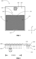
- FIG. 1 illustratively shows an example of the diffractive optical waveguide 100 for optical pupil expansion according to an embodiment of the present invention, namely the diffractive optical waveguide 100.
- the diffractive optical waveguide 100 comprises a waveguide substrate 110.
- the waveguide substrate 110 can be made of glass, optical plastic, or other optical transmission materials.
- the waveguide substrate 110 can have first and second substantially flat surfaces 111, 112, wherein the first surface 111 is opposite to the second surface 112, wherein the first surface 111 can be the surface of the display device with the waveguide substrate 110 on the side facing the viewer's eyes.
- the waveguide substrate 110 With the waveguide substrate 110, light may propagate in a direction substantially parallel to the first surface 111 and the second surface 112 by total internal reflection.
- the diffractive optical waveguide 100 of the present invention further comprises a coupling-in grating 120 and a coupling-out grating 130, wherein the coupling-in grating 120 is disposed on or in the waveguide substrate 110 and is configured to couple the input light into the waveguide substrate 110 to allow it to be coupled to the coupling-out grating 130 by total reflection.
- the coupling-out grating 130 is disposed on or in the waveguide substrate 110 and is configured to couple input light out of the waveguide substrate 110 by diffraction to allow the viewer's eyes to receive the coupled-out light.
- the light entering into the coupling-in grating 120 is, for example, the image light projected by a projector
- the light coupled out of the coupling-out grating 130 is at least a portion of the image light, and the portion of the image light is guided to the viewer's eyes through the coupling-out grating 130, such that the image projected by the projector is visible to the viewer's eyes.
- the coupling-out grating 130 serves as pupil expansion, which can refer to an input of a low field of view (FOV) being changed into an output of a high FOV.
- FOV low field of view
- the coupling-in grating 120 and the coupling-out grating 130 can be located on the same side of the waveguide substrate 110, for example, both are disposed on the first surface 111 of the waveguide substrate 110, or can be located on either side, i.e., on the first surface 111 and the second surface 112, respectively.
- the diffractive optical waveguide 100 can further comprise a turning grating, whereby light is coupled into the waveguide substrate 110 through the coupling-in grating 120 and into the turning grating through the waveguide substrate 110 by total reflection, and propagates through the turning grating in a first predetermined direction and then is coupled out of the coupling-out grating 130 in a second predetermined direction, wherein the first predetermined direction is different from the second predetermined direction.
- a turning grating whereby light is coupled into the waveguide substrate 110 through the coupling-in grating 120 and into the turning grating through the waveguide substrate 110 by total reflection, and propagates through the turning grating in a first predetermined direction and then is coupled out of the coupling-out grating 130 in a second predetermined direction, wherein the first predetermined direction is different from the second predetermined direction.
- the coupling-in grating 120 and the coupling-out grating 130 are located on the same side surface of the waveguide substrate 110.
- the coupling-in grating 120 can be a one-dimensional grating, such as a linear grating, or a slanted grating, a non-blazed grating, and other suitable types of gratings, or the coupling-in grating 120 can also be a metasurface coupling-in structure.
- the coupling-in grating 120 can also be implemented by some other optical devices having coupling function, such as a prism, a reflective polarizer, or a mirror with reflection function.
- the coupling-in grating 120 can be an optical element including a periodic structure, which can be fabricated by any suitable microfabrication process.
- the grating can be fabricated on the surface of or inside the waveguide substrate 110 by photolithography, or on the waveguide substrate 110 by nanoimprint lithography, thereby forming a surface relief diffraction grating.
- the coupling-out grating 130 can comprise a first coupling-out region 131, a second coupling-out region 132 and a third coupling-out grating 133, which are all arranged successively in the first direction L1, wherein the second coupling-out region 132 may be disposed between the first coupling-out region 131 and the third coupling-out region 133.
- At least one of the first coupling-out grating 131 and the third coupling-out grating 133 may be a one-dimensional grating structure.
- the second coupling-out grating 132 may be a two-dimensional grating structure.
- the two-dimensional grating structure comprises a plurality of two-dimensional periodic structures.
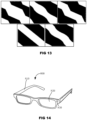
- the two-dimensional periodic structure of the two-dimensional grating can be in the shape of a polygon, such as a quadrilateral, a pentagon, a hexagon, and other polygons, etc., and may also be a triangle or Reuleaux Triangle, with reference to FIG. 12 .
- the second coupling-out grating 132 can be configured such that a minority of light into the second coupling-out grating 132 is coupled out of the waveguide substrate 110 toward the viewer's eyes, and the majority of the light into the second coupling-out grating 132 propagate by diffraction toward the region where the first coupling-out grating 131, the second coupling-out grating 132, and the third coupling-out grating 133 are located.
- the first coupling-out grating 131 and the third coupling-out grating 133 are configured such that a part of light out of the waveguide substrate 110 is coupled toward the viewer's eyes, and the other part of light can also propagate toward the second coupling-out grating 132 to at least fill light in the boundary areas between the second coupling-out grating 132 and the first coupling-out grating 131, as well as in the boundary areas between the second coupling-out grating 132 and the third coupling-out grating 133. In this way, it is possible to avoid the emergence of clear demarcation for bright and dark in the boundary areas.
- the coupling-out grating 130 can be fabricated by any suitable microfabrication process.
- the grating can be fabricated on the surface or inside of the waveguide substrate 110 by photolithography, or on the waveguide substrate 110 by nanoimprint lithography, thereby forming a surface relief diffraction grating.
- the central axis A1 of the coupling-in grating 120 is parallel to the second direction L2, wherein the second direction L2 is orthogonal to the first direction L1.
- the first coupling-out grating 131 is symmetric to the third coupling-out grating 133 with respect to the central axis A1.
- the second coupling-out grating 132 is also symmetric with respect to the central axis A1. It will be appreciated that in other embodiments, the first coupling-out grating 131 can be not symmetric to the third coupling-out grating 133, and the second coupling-out grating 132 can be in asymmetric shape.
- the second coupling-out grating 132 is corresponding to a region that includes a first edge 136 and a second edge 137 spaced in a second direction L2. Moreover, the first edge 136 is closer to the coupling-in grating 120 than the second edge 137. In other words, the second edge 137 is further away from the coupling-in grating 120 than the first edge 136.
- the first width of the first edge 136 in the first direction L1 is greater than a second width of the second edge 137 in the first direction L1.
- the first width of the first edge 136 is configured so that an periphery field-of-view light in the field of view formed by the light output from the coupling-in grating120 can be incident into the second coupling-out grating 132 through total reflection by the waveguide substrate 110.
- the second width of the second edge 137 is greater than or equal to 0.
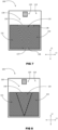
- the second coupling-out grating 132 is located in a region generally shaped as a triangle (as shown in FIG. 8 ).
- the second coupling-out grating 132 is located in a region generally shaped as an inverted trapezoid (as shown in FIG. 1 ) or the combination of an inverted trapezoid and a rectangle (as shown in FIG. 6 ).
- a chamfer 138 can be disposed in the second coupling-out grating 132 in its vicinity to the first edge 136 and in its vicinity to the second edge 137.
- the structures shown with reference to FIGS. 5 , 7 , and 9 correspond to the modifications of embodiments in FIGS. 1 , 6 , and 8 , respectively.
- the propagation direction of light in the diffractive optical waveguide 100 of the present invention will be described below with reference to FIG. 4 .
- the light incident into the second coupling-out grating 132 can be diffracted into a plurality of beam splits by the second coupling-out grating 132, for example, the first beam split D1, the second beam split D2, and the third beam split D3.
- the first beam split D1 propagates in the region of the second coupling-out grating 132.
- the second beam split D2 propagates toward either the first coupling-out grating 131 or the third coupling-out grating 133, e.g., toward the first coupling-out grating 131 as depicted in the figure.
- the third beam split D3 continues to propagate in the original direction, that is, the third beam split D3 propagates in the same direction as same as the propagation direction of the light output from the coupling-in grating 120. Therefore, the third beam split D3 can enter the first coupling-out grating 131 or the third coupling-out grating 133 in the original propagation direction.
- the third beam split D3 can be diffracted by the first coupling-out grating 131 into a first light component and a second light component.
- the first light component propagates in the first coupling-out grating 131 and is at least partially coupled out of the waveguide substrate 110, while the second light component propagates toward the second coupling-out grating 132 to fill light in the second coupling-out grating 132.
- the third beam split D3 After the third beam split D3 enters the third coupling-out grating 133 in the original propagation direction, the third beam split D3 is diffracted by the third coupling-out grating 133 into a first light component and a second light component.
- the first light component propagates in the third coupling-out grating 133 and is at least partially coupled out of the waveguide substrate 110, and the second light component propagates toward the second coupling-out grating 132 for filling light in the second coupling-out grating 132.
- a first field-of-view angle is defined as the included angle between the periphery field-of-view light and the central axis A1 of the coupling-in grating 120.
- the first width of the first edge 136 is determined depending on the width of the coupling-in grating 120 in the first direction L1, the distance between the first edge 136 and the center of the coupling-in grating 120, and the first field-of-view angle.
- the first width of the first edge 136 can also be adjusted by adjusting the value of ⁇ .
- a first included angle ⁇ is defined between the second edge 137 and the line connecting respective endpoints of the first edge 136 and the second edge 137 located on the same side with respect to the central axis A1 of the second coupling-out grating 132, and a second included angle ⁇ is defined between the second edge 137 and the propagation direction of the first beam split D1.
- the first included angle ⁇ is greater than or equal to the second included angle ⁇ , that is, ⁇ .
- the first included angle ⁇ can be an acute angle formed by the leg of the inverted trapezoid and the straight line of the second edge 137.
- the width of the second edge 137 should be able to satisfy the above relationship between the first included angle ⁇ and the second included angle ⁇ .
- the region of the second coupling-out grating 132 being shaped as an inverted trapezoid for example, , with reference to FIG.
- the third width is defined as the length of the coupling-out grating in the second direction L2 being divided by the tangent value of the first included angle ⁇ , whereby the second width of the second edge 137 is required to be less than the difference between the first width of the first edge 136 and the double of the third width.
- the coupling-out grating 130 can further include the fourth coupling-out grating 134 and the fifth coupling-out grating 135, referring to FIG. 10 and FIG. 11 .
- the fourth coupling-out grating 134 is disposed between the first coupling-out grating 131 and the second coupling-out grating 132
- the fifth coupling-out grating 135 is disposed between the second coupling-out grating 132 and the third coupling-out grating 133.
- the fourth coupling-out grating 134 is symmetric to the fifth coupling-out grating 135 with respect to the central axis A1 of the second coupling-out grating 132.
- the fourth and fifth coupling-out gratings 134 and 135 each can include a plurality of grating lines.
- the fourth and fifth coupling-out gratings 134 and 135 each can be a one-dimensional grating different from the first coupling-out grating 131 and the third coupling-out grating 133. That is, the above grating lines can be constructed as linear structure as shown in FIG. 13 ; or the fourth coupling-out grating 134 and the fifth coupling-out grating 135 can also be two-dimensional gratings tending to be like one-dimensional gratings, so as to avoid sudden optical change generated between one-dimensional and two-dimensional regions.
- each of the grating lines comprises a plurality of periodic structures in continuous and connected arrangement. At least one side edge of the periodic structures is a non-linear side edge.
- the shape of the non-linear side edge is one of a polyline, an arc, a combination of a straight line and an arc, and any other suitable shape structures.
- the polyline shape can have one or more bends; the arc shape can be in the form of an arc or several arcs connected one by one; the combination of the straight line and arc can also be in the form of a straight line connected with an arc, or several straight lines and an arc connected one by one, or several straight lines and several arcs connected one by one.
- the bend angle of polyline-shaped non-linear side edge and the curving radian of arc-shaped non-linear side edge can be adjusted depending on actual needs, and are not specifically limited here.
- the periodic structure of the grating lines may be freely selected from the structure shown in FIG. 13 , which are not limited here.
- the second coupling-out grating 132 includes multiple sub-regions. As shown in FIG. 10 , the second coupling-out grating 132 includes the first sub-region 1321 and the second sub-region 1322 arranged in the second direction L2. The second coupling-out grating 132 as shown in FIG. 11 includes three sub-regions, namely the first sub-region1321, the third sub-region 1323, and the second sub-region1322 arranged in the second direction L2.
- different sub-regions of the second coupling-out grating 132 have different two-dimensional periodic structures.
- the first sub-region 1321 and the second sub-region 1322 in FIG. 10 have respective, different two-dimensional periodic structures.
- the first sub-region 1321, the second sub-region 1322, and the third sub-region 1323 as shown in FIG. 11 have respective, different two-dimensional periodic structures.
- At least two sub-regions of the multiple sub-regions have the same shape.
- the first sub-region 1321 and the second sub-region 1322 as shown in FIG. 10 can adopt the same two-dimensional periodic structure.
- the first sub-region 1321 and the second sub-region 1322 as shown in FIG. 11 can adopt the same two-dimensional periodic structure, while the third sub-region 1323 can be different.
- the present invention also provides a display device 800, which may comprise the aforementioned diffractive optical waveguide 100, wherein the description of the diffractive optical waveguide 100 can be referenced from the above and will not be repeated here.
- the display device 800 can be any device comprising the aforementioned diffractive optical waveguide 100.
- the display device 800 can be a near-eye display device, which may comprise a lens 820 and a frame 810 for holding the lens near eyes, the lens 820 including the diffractive optical waveguide 100.
- the display device 800 may further comprise an optical source 830.
- the optical source 830 can project image light onto the diffractive optical waveguide 100, e.g., into the area where the coupling-in grating 120 of the diffractive optical waveguide 100 is located.
- the optical source 830 can be micro displays, such as a laser beam scanning (LBS), a digital light procession (DLP), a digital micromirror device (DMD), a liquid crystal on silicon (LCOS), a micro electromechanical system (MEMS), an organic light emitting diode (OLED), or the like.
- LBS laser beam scanning
- DLP digital light procession
- DMD digital micromirror device
- LCOS liquid crystal on silicon
- MEMS micro electromechanical system
- OLED organic light emitting diode
- the light (e.g., image light) projected by the optical source 830 onto the diffractive optical waveguide 100 is coupled into the waveguide substrate 110 through the coupling-in grating 120 and to the coupling-out grating 130 by totally reflection.
- the light is coupled out of the coupling-out grating 130 and comes into the eyes of viewer wearing the near-eye device, such that the image projected by the optical source 830 is visible to the viewer's eyes.
- the second coupling-out grating 132 being disposed between the first coupling-out grating 131 and the third coupling-out grating 133, and the width of the first edge 136 of the second coupling-out grating 132 being greater than the width of the second edge 137, it is possible to obtain a better effect of two-dimensional pupil expansion using the second coupling-out grating 132, while the coupling-out efficiency can be improved using the first coupling-out grating 131 and the third coupling-out grating 133, so as to achieve the effect of higher uniformity between different regions being compatible with higher overall coupling-out efficiency.
- the display device 800 is an augmented reality display device or a virtual reality display device, wherein the augmented reality display device includes but is not limited to the devices such as augmented reality (AR) glasses, an automotive head-up display (HUD), or the like.
- AR augmented reality
- HUD automotive head-up display
Landscapes
- Physics & Mathematics (AREA)
- General Physics & Mathematics (AREA)
- Optics & Photonics (AREA)
- Optical Couplings Of Light Guides (AREA)
- Optical Integrated Circuits (AREA)
Claims (17)
- Guide d'onde optique diffractif (100) pour une dilatation de pupille optique, comprenant :un substrat de guide d'onde (110) ;un réseau de couplage d'entrée (120) disposé sur ou dans le substrat de guide d'onde et configuré pour coupler la lumière d'entrée dans le substrat de guide d'onde, afin de provoquer la propagation de la lumière dans le substrat de guide d'onde par le biais d'une réflexion totale ;un réseau de couplage de sortie (130) disposé sur ou dans le substrat de guide d'onde, et configuré pour un couplage de sortie d'au moins une portion de la lumière se propageant à l'intérieur de celui-ci à partir du substrat de guide d'onde par diffraction, dans lequelle réseau de couplage de sortie comprend un premier réseau de couplage de sortie (131), un deuxième réseau de couplage de sortie (132), et un troisième réseau de couplage de sortie (133), ceux-ci étant tous agencés de manière successive dans une première direction (L1) ; le deuxième réseau de couplage de sortie est disposé entre le premier réseau de couplage de sortie et le troisième réseau de couplage de sortie, et comprend un réseau bidimensionnel ; le deuxième réseau de couplage de sortie correspond à une région, laquelle inclut un premier bord (136) et un second bord (137) espacé dans une seconde direction (L2) orthogonale à la première direction, et dans lequel le premier bord est plus proche du réseau de couplage d'entrée que le second bord ; la lumière produite par le réseau de couplage d'entrée est incidente sur le deuxième réseau de couplage de sortie par le biais du substrat de guide d'onde, et est diffractée par le deuxième réseau de couplage de sortie en une pluralité de faisceaux divisés, la pluralité de faisceaux divisés inclut un premier faisceau divisé se propageant dans la région du deuxième réseau de couplage de sortie, un deuxième faisceau divisé se propageant vers le premier réseau de couplage de sortie ou le troisième réseau de couplage de sortie, et un troisième faisceau divisé se propageant dans la même direction que la direction de propagation de la lumière produite par le réseau de couplage d'entrée, et le troisième faisceau divisé peut être propagé vers le premier réseau de couplage de sortie ou le troisième réseau de couplage de sortie,caractérisé en ce qu'une première largeur du premier bord dans la première direction est supérieure à une deuxième largeur du second bord dans la première direction.
- Guide d'onde optique diffractif selon la revendication 1, dans lequel le réseau de couplage d'entrée présente un axe central parallèle à la seconde direction ; un premier angle inclus est défini entre le second bord et une ligne reliant des points terminaux respectifs du premier bord et du second bord du deuxième réseau de couplage de sortie sur le même côté de l'axe central, et un second angle inclus est défini entre le second bord et la direction de propagation du premier faisceau divisé, et dans lequel le premier angle inclus est supérieur ou égal au second angle inclus.
- Guide d'onde optique diffractif selon la revendication 1, dans lequel le troisième faisceau divisé est diffracté en une première composante de lumière et une seconde composante de lumière par le premier réseau de couplage de sortie ; dans lequel la première composante de lumière se propage dans le premier réseau de couplage de sortie et est au moins en partie couplée à la sortie du substrat de guide d'onde, et la seconde composante de lumière se propage vers le deuxième réseau de couplage de sortie pour un remplissage de lumière, ou
le troisième faisceau divisé est diffracté en une première composante de lumière et une seconde composante de lumière par le troisième réseau de couplage de sortie ; dans lequel la première composante de lumière se propage dans le troisième réseau de couplage de sortie et est au moins en partie couplée à la sortie du substrat de guide d'onde, et la seconde composante de lumière se propage vers le deuxième réseau de couplage de sortie pour un remplissage de lumière. - Guide d'onde optique diffractif selon la revendication 1, dans lequel la première largeur du premier bord est configurée de sorte que la lumière de champ de vision de périphérie dans le champ de vision formé par la lumière produite à partir du réseau de couplage d'entrée peut être incidente dans le deuxième réseau de couplage de sortie par le biais d'une réflexion totale par le substrat de guide d'onde.
- Guide d'onde optique diffractif selon la revendication 4, dans lequel un premier angle de champ de vision est défini comme un angle inclus entre la lumière de champ de vision de périphérie et l'axe central du réseau de couplage d'entrée, et l'axe central du réseau de couplage d'entrée est parallèle à la seconde direction ; la première largeur du premier bord est déterminée sur la base d'une largeur du réseau de couplage d'entrée dans la première direction, d'une distance entre le premier bord et un centre du réseau de couplage d'entrée, et du premier angle de champ de vision.
- Guide d'onde optique diffractif selon la revendication 5, dans lequel la première largeur du premier bord est calculée à partir de la formule suivante :

- Guide d'onde optique diffractif selon la revendication 2, dans lequel la deuxième largeur du second bord est inférieure à une différence entre la première largeur du premier bord et le double d'une troisième largeur, et la troisième largeur est définie comme une longueur du réseau de couplage de sortie dans la seconde direction étant divisée par une valeur de tangente du premier angle inclus.
- Guide d'onde optique diffractif selon la revendication 1, dans lequel le premier réseau de couplage de sortie et le troisième réseau de couplage de sortie sont chacun un réseau unidimensionnel.
- Guide d'onde optique diffractif selon la revendication 1, dans lequel un axe central du réseau de couplage d'entrée est parallèle à la seconde direction ; le premier réseau de couplage de sortie est symétrique au troisième réseau de couplage de sortie par rapport à l'axe central, et le deuxième réseau de couplage de sortie est symétrique par rapport à l'axe central.
- Guide d'onde optique diffractif selon la revendication 1, dans lequel le deuxième réseau de couplage de sortie comprend une pluralité de sous-régions ; des réseaux de couplage de sortie dans des sous-régions différentes présentent des structures périodiques bidimensionnelles différentes, ou
des réseaux de couplage de sortie d'au moins deux sous-régions de la pluralité des sous-régions présentent des structures périodiques bidimensionnelles identiques. - Guide d'onde optique diffractif selon l'une quelconque des revendications 1 à 10, dans lequel la deuxième largeur du second bord est supérieure ou égale à 0.
- Guide d'onde optique diffractif selon l'une quelconque des revendications 1 à 10, dans lequel le deuxième réseau de couplage de sortie se trouve dans une région prenant la forme d'un des éléments suivants : un trapézoïde inversé, un triangle, et une combinaison entre un trapézoïde inversé et un rectangle.
- Guide d'onde optique diffractif selon l'une quelconque des revendications 1 à 10, dans lequel un chanfrein est disposé dans le deuxième réseau de couplage de sortie dans son voisinage avec le premier bord, et/ou un chanfrein est disposé dans le deuxième réseau de couplage de sortie dans son voisinage avec le second bord.
- Guide d'onde optique diffractif selon l'une quelconque des revendications 1 à 10, dans lequel le réseau de couplage de sortie comprend en outre un quatrième réseau de couplage de sortie et un cinquième réseau de couplage de sortie ; le quatrième réseau de couplage de sortie est disposé entre le premier réseau de couplage de sortie et le deuxième réseau de couplage de sortie, et le cinquième réseau de couplage de sortie est disposé entre le deuxième réseau de couplage de sortie et le troisième réseau de couplage de sortie, et dans lequel le quatrième réseau de couplage de sortie est symétrique au cinquième réseau de couplage de sortie par rapport à un axe central du deuxième réseau de couplage de sortie.
- Guide d'onde optique diffractif selon la revendication 14, dans lequel le quatrième réseau de couplage de sortie et le cinquième réseau de couplage de sortie comprennent chacun une pluralité de lignes de réseau ; chacune des lignes de réseau comprend une pluralité de structures périodiques suivant un agencement continu et connecté ; au moins un bord des structures périodiques est un bord non linéaire, et la forme du bord non linéaire est un élément parmi : une polyligne, un arc, et une combinaison entre une ligne droite et un arc.
- Dispositif d'affichage, comprenant le guide d'onde optique diffractif selon l'une quelconque des revendications 1 à 15.
- Dispositif d'affichage selon la revendication 16, dans lequel le dispositif d'affichage est un dispositif d'affichage proche de l'œil, comprenant une lentille et un cadre pour tenir la lentille proche des yeux, la lentille incluant le guide d'onde optique diffractif.
Applications Claiming Priority (1)
| Application Number | Priority Date | Filing Date | Title |
|---|---|---|---|
| CN202210399540.6A CN114910991B (zh) | 2022-04-15 | 2022-04-15 | 衍射光波导及显示设备 |
Publications (3)
| Publication Number | Publication Date |
|---|---|
| EP4300165A1 EP4300165A1 (fr) | 2024-01-03 |
| EP4300165B1 true EP4300165B1 (fr) | 2025-03-05 |
| EP4300165C0 EP4300165C0 (fr) | 2025-03-05 |
Family
ID=82765165
Family Applications (1)
| Application Number | Title | Priority Date | Filing Date |
|---|---|---|---|
| EP23167554.7A Active EP4300165B1 (fr) | 2022-04-15 | 2023-04-12 | Guide d'ondes optique diffractif et dispositif d'affichage |
Country Status (3)
| Country | Link |
|---|---|
| US (1) | US11841523B2 (fr) |
| EP (1) | EP4300165B1 (fr) |
| CN (1) | CN114910991B (fr) |
Families Citing this family (14)
| Publication number | Priority date | Publication date | Assignee | Title |
|---|---|---|---|---|
| US12140754B2 (en) * | 2021-12-30 | 2024-11-12 | Goertek Inc. | Optical display system and augmented reality electronic device |
| CN114545549B (zh) * | 2022-01-13 | 2023-05-30 | 嘉兴驭光光电科技有限公司 | 用于衍射显示的光学波导装置及显示设备 |
| CN116699751B (zh) * | 2022-02-28 | 2024-05-24 | 荣耀终端有限公司 | 光波导及近眼显示设备 |
| CN115128720B (zh) * | 2022-08-30 | 2022-11-29 | 北京亮亮视野科技有限公司 | 二维超表面光栅、光波导、显示装置和头戴式设备 |
| CN115793132B (zh) * | 2023-01-29 | 2023-07-25 | 北京亮亮视野科技有限公司 | 二维衍射光栅波导结构和近眼显示设备 |
| FI131791B1 (en) * | 2023-05-04 | 2025-12-02 | Dispelix Oy | Display structure |
| CN116256836B (zh) * | 2023-05-16 | 2023-07-18 | 驭光科技(北京)有限公司 | 衍射光波导和显示设备 |
| EP4474695B1 (fr) * | 2023-06-08 | 2026-04-29 | Snap, Inc. | Dispositif optique pour affichage de réalité augmentée ou de réalité virtuelle |
| CN119224912A (zh) * | 2023-06-29 | 2024-12-31 | 歌尔光学科技(上海)有限公司 | 导光器件、光学模组以及头戴显示设备 |
| CN117872523B (zh) * | 2024-03-12 | 2024-07-02 | 北京亮亮视野科技有限公司 | 基于微纳结构的光波导系统和显示设备 |
| CN118377081B (zh) | 2024-06-26 | 2024-10-01 | 歌尔光学科技有限公司 | 导光器件、光学显示系统及显示设备 |
| CN118625440B (zh) * | 2024-08-09 | 2024-12-20 | 北京亮亮视野科技有限公司 | 超表面光栅波导及增强现实显示设备 |
| CN119439363A (zh) * | 2024-11-27 | 2025-02-14 | 深圳市光舟半导体技术有限公司 | 光波导及显示设备 |
| CN119828284B (zh) * | 2025-02-18 | 2025-11-25 | 北京至格科技有限公司 | 一种双目显示衍射光波导装置 |
Family Cites Families (9)
| Publication number | Priority date | Publication date | Assignee | Title |
|---|---|---|---|---|
| EP3933490B1 (fr) * | 2019-03-13 | 2024-06-12 | Lg Chem, Ltd. | Plaque de guidage de lumière à diffraction |
| JP7560887B2 (ja) * | 2019-04-16 | 2024-10-03 | ディスペリックス オサケ ユキチュア | 新規な格子配置 |
| US20210063765A1 (en) * | 2019-08-28 | 2021-03-04 | Aac Optics Solutions Pte. Ltd. | Waveguide-based augmented reality display apparatus |
| CN111240015B (zh) * | 2020-01-17 | 2020-12-18 | 北京理工大学 | 双侧对射出光均匀的衍射波导 |
| CN213690000U (zh) * | 2020-10-28 | 2021-07-13 | 歌尔股份有限公司 | 光波导和ar设备 |
| CN215264107U (zh) * | 2021-07-26 | 2021-12-21 | Oppo广东移动通信有限公司 | 波导组件、光学装置及智能眼镜 |
| CN119828288B (zh) * | 2021-07-30 | 2025-10-28 | Oppo广东移动通信有限公司 | 光学结构和光学装置 |
| CN113777707B (zh) * | 2021-09-16 | 2024-02-13 | Oppo广东移动通信有限公司 | 光学结构和光学装置 |
| CN114296244B (zh) * | 2022-02-18 | 2024-04-19 | 杭州海康威视数字技术股份有限公司 | 用于近眼显示的光波导以及近眼显示设备 |
-
2022
- 2022-04-15 CN CN202210399540.6A patent/CN114910991B/zh active Active
-
2023
- 2023-04-11 US US18/132,982 patent/US11841523B2/en active Active
- 2023-04-12 EP EP23167554.7A patent/EP4300165B1/fr active Active
Also Published As
| Publication number | Publication date |
|---|---|
| EP4300165A1 (fr) | 2024-01-03 |
| CN114910991B (zh) | 2023-03-24 |
| US20230333301A1 (en) | 2023-10-19 |
| US11841523B2 (en) | 2023-12-12 |
| CN114910991A (zh) | 2022-08-16 |
| EP4300165C0 (fr) | 2025-03-05 |
Similar Documents
| Publication | Publication Date | Title |
|---|---|---|
| EP4300165B1 (fr) | Guide d'ondes optique diffractif et dispositif d'affichage | |
| EP4310576B1 (fr) | Guide d'ondes optique diffractif et dispositif d'affichage | |
| US11874503B1 (en) | Diffractive optical waveguide and display device | |
| CN113985616B (zh) | 光波导显示器件和增强现实显示设备 | |
| CN109387941B (zh) | 光学窗系统和包括其的透视型显示装置 | |
| US11960087B2 (en) | Optical device and display apparatus with same images for left and right eyes | |
| US11988838B2 (en) | Diffractive optical waveguide and display device | |
| US11624869B2 (en) | Optical expander device for providing an extended field of view | |
| EP2153266B1 (fr) | Expanseur de faisceau diffractif et afficheur virtuel basé sur un expanseur de faisceau diffractif | |
| US11789261B2 (en) | Optical expander device for displaying wide color image, display device thereof, and method for outputting light and displaying an image | |
| JP2006510059A (ja) | 回折効率のバランスをとるための回折格子素子 | |
| EP4418031A1 (fr) | Guide d'ondes optique diffractif et dispositif d'affichage | |
| CN111175971A (zh) | 一种近眼光学显示系统、增强现实眼镜 | |
| US20240126093A1 (en) | Display apparatus | |
| JP4717196B2 (ja) | 画像観察装置および画像観察システム | |
| US20210302752A1 (en) | Near-eye display devices | |
| US12222533B1 (en) | Optical waveguide device and display device | |
| CN113692549B (zh) | 全息导波器 | |
| CN115461667B (zh) | 光学装置 |
Legal Events
| Date | Code | Title | Description |
|---|---|---|---|
| PUAI | Public reference made under article 153(3) epc to a published international application that has entered the european phase |
Free format text: ORIGINAL CODE: 0009012 |
|
| STAA | Information on the status of an ep patent application or granted ep patent |
Free format text: STATUS: THE APPLICATION HAS BEEN PUBLISHED |
|
| AK | Designated contracting states |
Kind code of ref document: A1 Designated state(s): AL AT BE BG CH CY CZ DE DK EE ES FI FR GB GR HR HU IE IS IT LI LT LU LV MC ME MK MT NL NO PL PT RO RS SE SI SK SM TR |
|
| STAA | Information on the status of an ep patent application or granted ep patent |
Free format text: STATUS: REQUEST FOR EXAMINATION WAS MADE |
|
| 17P | Request for examination filed |
Effective date: 20240405 |
|
| RBV | Designated contracting states (corrected) |
Designated state(s): AL AT BE BG CH CY CZ DE DK EE ES FI FR GB GR HR HU IE IS IT LI LT LU LV MC ME MK MT NL NO PL PT RO RS SE SI SK SM TR |
|
| GRAP | Despatch of communication of intention to grant a patent |
Free format text: ORIGINAL CODE: EPIDOSNIGR1 |
|
| STAA | Information on the status of an ep patent application or granted ep patent |
Free format text: STATUS: GRANT OF PATENT IS INTENDED |
|
| INTG | Intention to grant announced |
Effective date: 20240619 |
|
| GRAJ | Information related to disapproval of communication of intention to grant by the applicant or resumption of examination proceedings by the epo deleted |
Free format text: ORIGINAL CODE: EPIDOSDIGR1 |
|
| STAA | Information on the status of an ep patent application or granted ep patent |
Free format text: STATUS: REQUEST FOR EXAMINATION WAS MADE |
|
| GRAP | Despatch of communication of intention to grant a patent |
Free format text: ORIGINAL CODE: EPIDOSNIGR1 |
|
| STAA | Information on the status of an ep patent application or granted ep patent |
Free format text: STATUS: GRANT OF PATENT IS INTENDED |
|
| INTC | Intention to grant announced (deleted) | ||
| INTG | Intention to grant announced |
Effective date: 20241031 |
|
| GRAS | Grant fee paid |
Free format text: ORIGINAL CODE: EPIDOSNIGR3 |
|
| GRAA | (expected) grant |
Free format text: ORIGINAL CODE: 0009210 |
|
| STAA | Information on the status of an ep patent application or granted ep patent |
Free format text: STATUS: THE PATENT HAS BEEN GRANTED |
|
| AK | Designated contracting states |
Kind code of ref document: B1 Designated state(s): AL AT BE BG CH CY CZ DE DK EE ES FI FR GB GR HR HU IE IS IT LI LT LU LV MC ME MK MT NL NO PL PT RO RS SE SI SK SM TR |
|
| REG | Reference to a national code |
Ref country code: GB Ref legal event code: FG4D |
|
| REG | Reference to a national code |
Ref country code: CH Ref legal event code: EP |
|
| REG | Reference to a national code |
Ref country code: DE Ref legal event code: R096 Ref document number: 602023002271 Country of ref document: DE |
|
| REG | Reference to a national code |
Ref country code: IE Ref legal event code: FG4D |
|
| U01 | Request for unitary effect filed |
Effective date: 20250328 |
|
| U07 | Unitary effect registered |
Designated state(s): AT BE BG DE DK EE FI FR IT LT LU LV MT NL PT RO SE SI Effective date: 20250403 |
|
| U20 | Renewal fee for the european patent with unitary effect paid |
Year of fee payment: 3 Effective date: 20250423 |
|
| PG25 | Lapsed in a contracting state [announced via postgrant information from national office to epo] |
Ref country code: RS Free format text: LAPSE BECAUSE OF FAILURE TO SUBMIT A TRANSLATION OF THE DESCRIPTION OR TO PAY THE FEE WITHIN THE PRESCRIBED TIME-LIMIT Effective date: 20250605 |
|
| PG25 | Lapsed in a contracting state [announced via postgrant information from national office to epo] |
Ref country code: ES Free format text: LAPSE BECAUSE OF FAILURE TO SUBMIT A TRANSLATION OF THE DESCRIPTION OR TO PAY THE FEE WITHIN THE PRESCRIBED TIME-LIMIT Effective date: 20250305 |
|
| PG25 | Lapsed in a contracting state [announced via postgrant information from national office to epo] |
Ref country code: NO Free format text: LAPSE BECAUSE OF FAILURE TO SUBMIT A TRANSLATION OF THE DESCRIPTION OR TO PAY THE FEE WITHIN THE PRESCRIBED TIME-LIMIT Effective date: 20250605 |
|
| PG25 | Lapsed in a contracting state [announced via postgrant information from national office to epo] |
Ref country code: HR Free format text: LAPSE BECAUSE OF FAILURE TO SUBMIT A TRANSLATION OF THE DESCRIPTION OR TO PAY THE FEE WITHIN THE PRESCRIBED TIME-LIMIT Effective date: 20250305 |
|
| PG25 | Lapsed in a contracting state [announced via postgrant information from national office to epo] |
Ref country code: GR Free format text: LAPSE BECAUSE OF FAILURE TO SUBMIT A TRANSLATION OF THE DESCRIPTION OR TO PAY THE FEE WITHIN THE PRESCRIBED TIME-LIMIT Effective date: 20250606 |
|
| PG25 | Lapsed in a contracting state [announced via postgrant information from national office to epo] |
Ref country code: SM Free format text: LAPSE BECAUSE OF FAILURE TO SUBMIT A TRANSLATION OF THE DESCRIPTION OR TO PAY THE FEE WITHIN THE PRESCRIBED TIME-LIMIT Effective date: 20250305 |
|
| PG25 | Lapsed in a contracting state [announced via postgrant information from national office to epo] |
Ref country code: PL Free format text: LAPSE BECAUSE OF FAILURE TO SUBMIT A TRANSLATION OF THE DESCRIPTION OR TO PAY THE FEE WITHIN THE PRESCRIBED TIME-LIMIT Effective date: 20250305 |
|
| PG25 | Lapsed in a contracting state [announced via postgrant information from national office to epo] |
Ref country code: CZ Free format text: LAPSE BECAUSE OF FAILURE TO SUBMIT A TRANSLATION OF THE DESCRIPTION OR TO PAY THE FEE WITHIN THE PRESCRIBED TIME-LIMIT Effective date: 20250305 |
|
| PG25 | Lapsed in a contracting state [announced via postgrant information from national office to epo] |
Ref country code: SK Free format text: LAPSE BECAUSE OF FAILURE TO SUBMIT A TRANSLATION OF THE DESCRIPTION OR TO PAY THE FEE WITHIN THE PRESCRIBED TIME-LIMIT Effective date: 20250305 |
|
| PG25 | Lapsed in a contracting state [announced via postgrant information from national office to epo] |
Ref country code: IS Free format text: LAPSE BECAUSE OF FAILURE TO SUBMIT A TRANSLATION OF THE DESCRIPTION OR TO PAY THE FEE WITHIN THE PRESCRIBED TIME-LIMIT Effective date: 20250705 |
|
| PG25 | Lapsed in a contracting state [announced via postgrant information from national office to epo] |
Ref country code: MC Free format text: LAPSE BECAUSE OF FAILURE TO SUBMIT A TRANSLATION OF THE DESCRIPTION OR TO PAY THE FEE WITHIN THE PRESCRIBED TIME-LIMIT Effective date: 20250305 |
|
| PLBE | No opposition filed within time limit |
Free format text: ORIGINAL CODE: 0009261 |
|
| STAA | Information on the status of an ep patent application or granted ep patent |
Free format text: STATUS: NO OPPOSITION FILED WITHIN TIME LIMIT |
|
| REG | Reference to a national code |
Ref country code: CH Ref legal event code: L10 Free format text: ST27 STATUS EVENT CODE: U-0-0-L10-L00 (AS PROVIDED BY THE NATIONAL OFFICE) Effective date: 20260114 |
|
| 26N | No opposition filed |
Effective date: 20251208 |
|
| PG25 | Lapsed in a contracting state [announced via postgrant information from national office to epo] |
Ref country code: IE Free format text: LAPSE BECAUSE OF NON-PAYMENT OF DUE FEES Effective date: 20250412 |