EP4300587A1 - Feldeffekttransistor, herstellungsverfahren dafür und schaltkreis - Google Patents
Feldeffekttransistor, herstellungsverfahren dafür und schaltkreis Download PDFInfo
- Publication number
- EP4300587A1 EP4300587A1 EP22766220.2A EP22766220A EP4300587A1 EP 4300587 A1 EP4300587 A1 EP 4300587A1 EP 22766220 A EP22766220 A EP 22766220A EP 4300587 A1 EP4300587 A1 EP 4300587A1
- Authority
- EP
- European Patent Office
- Prior art keywords
- layer
- field effect
- effect transistor
- gallium nitride
- gate structure
- Prior art date
- Legal status (The legal status is an assumption and is not a legal conclusion. Google has not performed a legal analysis and makes no representation as to the accuracy of the status listed.)
- Pending
Links
Images


Classifications
-
- H—ELECTRICITY
- H10—SEMICONDUCTOR DEVICES; ELECTRIC SOLID-STATE DEVICES NOT OTHERWISE PROVIDED FOR
- H10D—INORGANIC ELECTRIC SEMICONDUCTOR DEVICES
- H10D62/00—Semiconductor bodies, or regions thereof, of devices having potential barriers
- H10D62/10—Shapes, relative sizes or dispositions of the regions of the semiconductor bodies; Shapes of the semiconductor bodies
- H10D62/102—Constructional design considerations for preventing surface leakage or controlling electric field concentration
- H10D62/103—Constructional design considerations for preventing surface leakage or controlling electric field concentration for increasing or controlling the breakdown voltage of reverse-biased devices
- H10D62/105—Constructional design considerations for preventing surface leakage or controlling electric field concentration for increasing or controlling the breakdown voltage of reverse-biased devices by having particular doping profiles, shapes or arrangements of PN junctions; by having supplementary regions, e.g. junction termination extension [JTE]
-
- H—ELECTRICITY
- H10—SEMICONDUCTOR DEVICES; ELECTRIC SOLID-STATE DEVICES NOT OTHERWISE PROVIDED FOR
- H10D—INORGANIC ELECTRIC SEMICONDUCTOR DEVICES
- H10D62/00—Semiconductor bodies, or regions thereof, of devices having potential barriers
- H10D62/80—Semiconductor bodies, or regions thereof, of devices having potential barriers characterised by the materials
- H10D62/85—Semiconductor bodies, or regions thereof, of devices having potential barriers characterised by the materials being Group III-V materials, e.g. GaAs
-
- H—ELECTRICITY
- H10—SEMICONDUCTOR DEVICES; ELECTRIC SOLID-STATE DEVICES NOT OTHERWISE PROVIDED FOR
- H10D—INORGANIC ELECTRIC SEMICONDUCTOR DEVICES
- H10D30/00—Field-effect transistors [FET]
- H10D30/01—Manufacture or treatment
- H10D30/015—Manufacture or treatment of FETs having heterojunction interface channels or heterojunction gate electrodes, e.g. HEMT
-
- H—ELECTRICITY
- H10—SEMICONDUCTOR DEVICES; ELECTRIC SOLID-STATE DEVICES NOT OTHERWISE PROVIDED FOR
- H10D—INORGANIC ELECTRIC SEMICONDUCTOR DEVICES
- H10D30/00—Field-effect transistors [FET]
- H10D30/40—FETs having zero-dimensional [0D], one-dimensional [1D] or two-dimensional [2D] charge carrier gas channels
- H10D30/47—FETs having zero-dimensional [0D], one-dimensional [1D] or two-dimensional [2D] charge carrier gas channels having two-dimensional [2D] charge carrier gas channels, e.g. nanoribbon FETs or high electron mobility transistors [HEMT]
-
- H—ELECTRICITY
- H10—SEMICONDUCTOR DEVICES; ELECTRIC SOLID-STATE DEVICES NOT OTHERWISE PROVIDED FOR
- H10D—INORGANIC ELECTRIC SEMICONDUCTOR DEVICES
- H10D30/00—Field-effect transistors [FET]
- H10D30/40—FETs having zero-dimensional [0D], one-dimensional [1D] or two-dimensional [2D] charge carrier gas channels
- H10D30/47—FETs having zero-dimensional [0D], one-dimensional [1D] or two-dimensional [2D] charge carrier gas channels having two-dimensional [2D] charge carrier gas channels, e.g. nanoribbon FETs or high electron mobility transistors [HEMT]
- H10D30/471—High electron mobility transistors [HEMT] or high hole mobility transistors [HHMT]
- H10D30/475—High electron mobility transistors [HEMT] or high hole mobility transistors [HHMT] having wider bandgap layer formed on top of lower bandgap active layer, e.g. undoped barrier HEMTs such as i-AlGaN/GaN HEMTs
-
- H—ELECTRICITY
- H10—SEMICONDUCTOR DEVICES; ELECTRIC SOLID-STATE DEVICES NOT OTHERWISE PROVIDED FOR
- H10D—INORGANIC ELECTRIC SEMICONDUCTOR DEVICES
- H10D64/00—Electrodes of devices having potential barriers
- H10D64/60—Electrodes characterised by their materials
- H10D64/62—Electrodes ohmically coupled to a semiconductor
-
- H—ELECTRICITY
- H10—SEMICONDUCTOR DEVICES; ELECTRIC SOLID-STATE DEVICES NOT OTHERWISE PROVIDED FOR
- H10D—INORGANIC ELECTRIC SEMICONDUCTOR DEVICES
- H10D84/00—Integrated devices formed in or on semiconductor substrates that comprise only semiconducting layers, e.g. on Si wafers or on GaAs-on-Si wafers
- H10D84/80—Integrated devices formed in or on semiconductor substrates that comprise only semiconducting layers, e.g. on Si wafers or on GaAs-on-Si wafers characterised by the integration of at least one component covered by groups H10D12/00 or H10D30/00, e.g. integration of IGFETs
- H10D84/82—Integrated devices formed in or on semiconductor substrates that comprise only semiconducting layers, e.g. on Si wafers or on GaAs-on-Si wafers characterised by the integration of at least one component covered by groups H10D12/00 or H10D30/00, e.g. integration of IGFETs of only field-effect components
-
- H—ELECTRICITY
- H10—SEMICONDUCTOR DEVICES; ELECTRIC SOLID-STATE DEVICES NOT OTHERWISE PROVIDED FOR
- H10W—GENERIC PACKAGES, INTERCONNECTIONS, CONNECTORS OR OTHER CONSTRUCTIONAL DETAILS OF DEVICES COVERED BY CLASS H10
- H10W74/00—Encapsulations, e.g. protective coatings
- H10W74/10—Encapsulations, e.g. protective coatings characterised by their shape or disposition
- H10W74/131—Encapsulations, e.g. protective coatings characterised by their shape or disposition the semiconductor body being only partially enclosed
- H10W74/137—Encapsulations, e.g. protective coatings characterised by their shape or disposition the semiconductor body being only partially enclosed the encapsulations being directly on the semiconductor body
-
- H—ELECTRICITY
- H10—SEMICONDUCTOR DEVICES; ELECTRIC SOLID-STATE DEVICES NOT OTHERWISE PROVIDED FOR
- H10D—INORGANIC ELECTRIC SEMICONDUCTOR DEVICES
- H10D62/00—Semiconductor bodies, or regions thereof, of devices having potential barriers
- H10D62/10—Shapes, relative sizes or dispositions of the regions of the semiconductor bodies; Shapes of the semiconductor bodies
- H10D62/17—Semiconductor regions connected to electrodes not carrying current to be rectified, amplified or switched, e.g. channel regions
- H10D62/343—Gate regions of field-effect devices having PN junction gates
-
- H—ELECTRICITY
- H10—SEMICONDUCTOR DEVICES; ELECTRIC SOLID-STATE DEVICES NOT OTHERWISE PROVIDED FOR
- H10D—INORGANIC ELECTRIC SEMICONDUCTOR DEVICES
- H10D62/00—Semiconductor bodies, or regions thereof, of devices having potential barriers
- H10D62/80—Semiconductor bodies, or regions thereof, of devices having potential barriers characterised by the materials
- H10D62/85—Semiconductor bodies, or regions thereof, of devices having potential barriers characterised by the materials being Group III-V materials, e.g. GaAs
- H10D62/8503—Nitride Group III-V materials, e.g. AlN or GaN
Definitions
- This application relates to the field of semiconductor technologies, and in particular, to a field effect transistor, a method for preparing the field effect transistor, and a switch circuit.
- a field effect transistor is widely used as a component of a circuit switch in various scenarios.
- GaN field effect transistor is switched on or off by controlling connection and cutoff of two-dimensional electron gas of a channel.
- GaN field effect transistors are generally classified into two types: normally-open field effect transistors that are also referred to as depletion-mode field effect transistors, and normally-closed field effect transistors that are also referred to as enhanced field effect transistors.
- a switch device is generally required to be a normally-closed device.
- a GaN field effect transistor provided in a current technology includes a channel layer, a source, a drain, a gate structure, and a gate metal layer.
- the gate metal layer supplies power to the gate structure, and conduction of the source and the drain is controlled by using the gate structure.
- the gate metal layer is generally in Schottky contact with the gate structure, and two back-to-back diodes are formed in the GaN field effect transistor. It is difficult to discharge a charge, and consequently, a threshold voltage of the field effect transistor is unstable.
- a Schottky diode between the gate metal layer and the gate structure is prone to break down when the gate metal layer withstands a relatively high voltage under a condition of a positive voltage bias.
- This application provides a field effect transistor, a method for preparing the field effect transistor, and a switch circuit, to improve threshold voltage stability and a breakdown capability of the field effect transistor.
- a field effect transistor is provided, where the field effect transistor is applied in a switch circuit and used as a main component of the switch circuit, and is configured to control connection and disconnection of the switch circuit.
- the field effect transistor includes a channel layer, a source, a drain, a gate structure, and a gate metal layer.
- the field effect transistor successively includes: a channel layer; a source, a drain, and a gate structure that are located on the channel layer and disposed at a same layer; and a gate metal layer located on the gate structure.
- the gate structure includes a P-type gallium nitride (pGaN) layer and an N-type gallium nitride (nGaN) layer that are disposed in a stacking manner, where the pGaN layer is located between the nGaN layer and the channel layer.
- pGaN P-type gallium nitride
- nGaN N-type gallium nitride
- an nGaN/pGaN reverse bias diode is used to replace a gate metal/pGaN Schottky diode in a current technology to withstand a voltage, so that a gate voltage-withstand capability of the field effect transistor can be greatly increased, thereby improving a breakdown capability of the field effect transistor.
- the gate metal layer is in ohmic contact with the nGaN layer.
- Forming ohmic contact between metal and a semiconductor means that a pure resistor is at a contact point, and smaller resistance is better, so that when a component is operated, most voltages are applied to an active area instead of a contact surface.
- the ohmic contact does not involve long-term thermo-electron bombardment, and is highly reliable.
- the gate metal layer is in ohmic contact with the gate structure, so that reliability of a connection between the gate metal layer and the gate structure can be improved, thereby improving reliability of the field effect transistor.
- a doping element of the pGaN layer may be magnesium (Mg) or the like, and a doping density of the pGaN layer is controlled between 1 ⁇ 10 18 cm -3 and 1 ⁇ 10 19 cm -3 , so that a charge storage effect during operation of a device can be reduced, carriers in the pGaN layer are exhausted as much as possible, and redundant-charge storage is avoided, thereby improving operating threshold voltage stability of the device.
- Mg magnesium
- a thickness of the pGaN layer may be reduced.
- the thickness of the pGaN layer is controlled to be between 50 nm and 70 nm, for example, 50 nm, 55 nm, 60 nm, 65 nm, or 70 nm. This is not limited herein.
- a doping element of the nGaN layer may be silicon (Si), germanium (Ge), or the like, and a doping density of the nGaN layer is controlled between 1 ⁇ 10 16 cm -3 and 5 x 10 19 cm -3 , so that a charge storage effect during operation of a device is reduced, carriers in the pGaN layer are exhausted as much as possible, and redundant-charge storage is avoided, thereby improving operating threshold voltage stability of the device.
- a thickness of the nGaN layer may be less than or equal to 40 nm. This is not limited herein.
- the field effect transistor may further include a substrate and a buffer layer disposed on the substrate, where the channel layer is formed on the buffer layer.
- the substrate is a basic component of the field effect transistor, and is configured to carry each function layer of the field effect transistor.
- the substrate may be made of different materials, provided that the substrate has a specific support strength.
- the substrate may be made of a material such as silicon, sapphire, silicon carbide, or gallium nitride, that is, the substrate may be made of different materials.
- a rectangular structure layer may be selected as the substrate.
- a shape of the substrate provided in embodiments of this application is not limited to a rectangular structure, and another shape such as an ellipse or a polygon may be used, provided that there is a sufficient area to carry another function layer of the field effect transistor.
- the buffer layer is disposed on the substrate, and may be specifically formed on a surface of the substrate by using a process such as chemical vapor deposition or epitaxial growth.
- the buffer layer serves as an optional structural layer.
- the buffer layer may be disposed based on a requirement. For example, when the substrate can directly carry the channel layer, the buffer layer may not be disposed, and the channel layer may be directly formed on the substrate; or when a material of the channel layer conflicts with that of the substrate, and the channel layer cannot be directly formed on the substrate, the buffer layer is disposed to isolate the substrate from the channel layer. In this case, the buffer layer is used as a bearer layer of the channel layer.
- the buffer layer When the buffer layer carries the channel layer, on one hand, the buffer layer can be used as a structural layer for carrying the channel layer; and on the other hand, the buffer layer further has elastic deformation performance to some extent and can protect the channel layer disposed on a surface of the buffer layer, thereby improving reliability and safety of the field effect transistor provided in embodiments of this application.
- the buffer layer may be made of a material such as gradient aluminum gallium nitride, super-lattice, or low-temperature aluminum nitride. During specific preparation of the field effect transistor, different materials may be selected based on a requirement to prepare the buffer layer.
- the channel layer is configured to form two-dimensional electron gas of the field effect transistor.
- the channel layer includes a gallium nitride (GaN) layer and an aluminum gallium nitride (AlGaN) barrier layer that are disposed in a stacking manner.
- GaN gallium nitride
- AlGaN aluminum gallium nitride
- a channel can be formed on a contact surface between the GaN layer and the AlGaN barrier layer, and the two-dimensional electron gas is located on the contact surface between the GaN layer and the AlGaN barrier layer.
- the GaN layer may be disposed on the buffer layer, for example, may be directly formed on the buffer layer by using an etching or ion injection process.
- the GaN layer may be directly prepared on the substrate by using a process such as etching or ion injection.
- the AlGaN barrier layer is disposed on a surface that is of the GaN layer and that is away from the substrate. During preparation, the AlGaN barrier layer may be prepared also by using the foregoing process such as etching or ion injection.
- the channel layer may further use another structure.
- the channel layer includes a three-layer structure: a gallium nitride layer, an aluminum gallium nitride barrier layer, and an aluminum nitride layer located between the gallium nitride layer and the aluminum gallium nitride barrier layer.
- a channel can also be formed by using the three-layer structure.
- the source, the drain, and the gate structure disposed at the same layer are functional layers of the field effect transistor.
- the source, the gate structure, and the drain are disposed on the channel layer and at the same layer, and are electrically connected to the channel layer.
- the source and the drain are respectively configured to connect to an external circuit, and the gate structure is configured to control connection and disconnection of a channel.
- the gate structure controls the channel to be connected, the field effect transistor is in a closed state, and the circuit connected to the source and the drain can be connected; or when the gate structure controls the channel to be disconnected, the field effect transistor is in a cutoff state, and the circuit connected to the source and the drain is in a disconnected state.
- the gate structure, the source, and the drain are respectively connected to the AlGaN barrier layer, and the source and the drain can be connected to the channel by using the AlGaN barrier layer.
- the gate structure can be connected to the channel by using the AlGaN barrier layer, and can absorb electrons located in the channel.
- the gate structure controls the channel to be connected electrons are located in the channel, and the source and the drain can be conducted by using electrons in the channel.
- the gate structure controls the channel to be disconnected electrons are absorbed by the gate structure, leaving no free electron in the channel, and the source and the drain are cut off.
- the gate structure is located between the source and the drain, and separates the source from the drain. It needs to be understood that, during specific disposition of the gate structure, the drain, and the source, the gate structure, the source, and the drain are disposed at intervals, to ensure electrical isolation between the gate structure, the source, and the drain.
- the gate metal layer is configured to connect to the gate structure, and is configured to apply, to the gate structure, a control voltage for controlling channel connection and disconnection.
- the field effect transistor may further include a passivation layer, where the passivation layer is configured to protect each functional layer in the field effect transistor.
- the passivation layer is disposed in a manner of stacking with the aluminum gallium nitride barrier. It needs to be understood that, to ensure that the source, the drain, and the gate structure can be connected to an external circuit and a control circuit, during disposition of the foregoing structures, the source, the drain, and the gate structure pass through the passivation layer and are exposed from the passivation layer. Exposed parts of the source, the drain, and the gate structure can be configured to connect to the external circuit and the control circuit.
- the passivation layer may be prepared by using silicon nitride, aluminum oxide, silicon oxynitride, or another insulation material.
- the passivation layer is an optional structural layer of the field effect transistor. When an application environment of the field effect transistor is relatively safe, the passivation layer may not be disposed.
- a method for preparing a field effect transistor includes the following steps: first forming a channel layer; then forming a gate structure on the channel layer, where the gate structure includes a P-type gallium nitride layer and an N-type gallium nitride layer that are disposed in a stacking manner, the P-type gallium nitride layer is located between the N-type gallium nitride layer and the channel layer, and a doping density of the P-type gallium nitride layer is between 1 ⁇ 10 18 cm -3 and 1 ⁇ 10 19 cm -3 ; and then forming a source and a drain on the channel layer, and forming a gate metal layer on the gate structure.
- a thickness of the P-type gallium nitride layer is greater than or equal to 50 nm and less than or equal to 70 nm.
- a switch circuit is provided, where the switch circuit includes a mainboard and a field effect transistor that is disposed on the mainboard and that is any one of the foregoing field effect transistors.
- a field effect transistor provided in embodiments of this application is widely used as a component of a circuit switch in various scenarios.
- a field effect transistor made of GaN (gallium nitride) series materials with high mobility and high chemical stability due to its material characteristics, can be used as a higher-frequency switch and therefore is widely used in a highfrequency circuit switch.
- GaN field effect transistor is switched on or off by controlling connection and cutoff of two-dimensional electron gas of a channel.
- GaN field effect transistors are generally classified into two types: normally-open field effect transistors that are also referred to as depletion-mode field effect transistors, and normally-closed field effect transistors that are also referred to as enhanced field effect transistors.
- a switch device is generally required to be a normally-closed device.
- a Schottky junction manner is used for connection between a gate metal layer and a gate structure of a current GaN field effect transistor, and two back-to-back diodes are formed in the GaN field effect transistor. It is difficult to discharge a charge, and consequently, a threshold voltage of the field effect transistor is unstable. In addition, a Schottky diode between the gate metal layer and the gate structure is prone to break down when the gate metal layer withstands a relatively high voltage under a condition of a positive voltage bias.
- an embodiment of this application provides a field effect transistor to improve threshold voltage stability and a breakdown capability of a device.
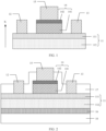
- FIG. 1 is a schematic diagram of a structure of a field effect transistor according to an embodiment of this application.
- the field effect transistor provided in this embodiment of this application includes a channel layer 11, a source 12, a drain 13, a gate structure 14, and a gate metal layer 15.
- a placement direction of the field effect transistor shown in FIG. 1 is used as a reference direction.
- the field effect transistor sequentially includes: a channel layer 11; a source 12, a drain 13, and a gate structure 14 that are located on the channel layer 11 and disposed at a same layer; and a gate metal layer 15 located on the gate structure 14.
- the gate structure 14 includes a P-type gallium nitride (pGaN) layer 141 and an N-type gallium nitride (nGaN) layer 142 that are disposed in a stacking manner, and the pGaN layer 141 is located between the nGaN layer 142 and the channel layer 11.
- pGaN P-type gallium nitride
- nGaN N-type gallium nitride
- the gate metal layer 15 is in ohmic contact with the nGaN layer 142.
- Forming ohmic contact between metal and a semiconductor means that a pure resistor is at a contact point, and smaller resistance is better, so that when a component is operated, most voltages are applied to an active area instead of a contact surface.
- the ohmic contact does not involve long-term thermo-electron bombardment, and is highly reliable.
- the gate metal layer is in ohmic contact with the gate structure, so that reliability of a connection between the gate metal layer and the gate structure can be improved, thereby improving reliability of the field effect transistor.
- a doping element of the pGaN layer 141 may be magnesium (Mg) or the like, and a doping density of the pGaN layer 141 is controlled between 1 ⁇ 10 18 cm -3 and 1 ⁇ 10 19 cm -3 , so that a charge storage effect during operation of a device can be reduced, carriers in the pGaN layer 141 are exhausted as much as possible, and redundant-charge storage is avoided, thereby improving operating threshold voltage stability of the device.
- Mg magnesium
- a thickness of the pGaN layer may be reduced.
- the thickness of the pGaN layer is controlled to be between 50 nm and 70 nm, for example, 50 nm, 55 nm, 60 nm, 65 nm, or 70 nm. This is not limited herein.
- a doping element of the nGaN layer 142 may be silicon (Si), germanium (Ge), or the like, and a doping density of the nGaN layer 142 is controlled between 1 x 10 16 cm -3 and 5 x 10 19 cm -3 , so that a charge storage effect during operation of a device is reduced, carriers in the pGaN layer are exhausted as much as possible, and redundant-charge storage is avoided, thereby improving operating threshold voltage stability of the device.
- a thickness of the nGaN layer 142 may be less than or equal to 40 nm. This is not limited herein.
- the field effect transistor may further include a substrate 10 and a buffer layer 16 disposed on the substrate 10, where the channel layer 11 is formed on the buffer layer 16.
- the substrate 10 is a basic component of the field effect transistor, and is configured to carry each function layer of the field effect transistor.
- the substrate 10 may be made of different materials, provided that the substrate 10 has a specific support strength.
- the substrate 10 may be made of a material such as silicon, sapphire, silicon carbide, or gallium nitride, that is, the substrate 10 may be made of different materials.
- a rectangular structure layer may be selected as the substrate 10.
- a shape of the substrate 10 provided in embodiments of this application is not limited to a rectangular structure, and another shape such as an ellipse or a polygon may be used, provided that there is a sufficient area to carry another function layer of the field effect transistor.
- the buffer layer 16 is disposed on the substrate 10, and may be specifically formed on a surface of the substrate 10 by using a process such as chemical vapor deposition or epitaxial growth.
- the buffer layer 16 serves as an optional structural layer.
- the buffer layer 16 may be disposed based on a requirement. For example, when the substrate 10 can directly carry the channel layer 11, the buffer layer 16 may not be disposed, and the channel layer 11 may be directly formed on the substrate 10; or when a material of the channel layer 11 conflicts with that of the substrate 10, and the channel layer 11 cannot be directly formed on the substrate 10, the buffer layer 16 is disposed to isolate the substrate 10 from the channel layer 11. In this case, the buffer layer 16 is used as a bearer layer of the channel layer 11.
- the buffer layer 16 When the buffer layer 16 carries the channel layer 11, on one hand, the buffer layer 16 can be used as a structural layer for carrying the channel layer 11; and on the other hand, the buffer layer 16 further has elastic deformation performance to some extent, and the buffer layer 16 can protect the channel layer 11 disposed on a surface of the buffer layer 16, thereby improving reliability and safety of the field effect transistor provided in embodiments of this application.
- the buffer layer 16 may be made of a material such as gradient aluminum gallium nitride, super-lattice, or low-temperature aluminum nitride. During specific preparation of the field effect transistor, different materials may be selected based on a requirement to prepare the buffer layer 16.
- the channel layer 11 is configured to form two-dimensional electron gas of the field effect transistor.
- the channel layer 11 includes a gallium nitride (GaN) layer 112 and an aluminum gallium nitride (AlGaN) barrier layer 111 that are stacked along the X direction.
- GaN gallium nitride
- AlGaN aluminum gallium nitride
- a channel can be formed on a contact surface between the GaN layer 112 and the AlGaN barrier layer 111, and the two-dimensional electron gas is located on the contact surface between the GaN layer 112 and the AlGaN barrier layer 111.
- the GaN layer 112 may be disposed on the buffer layer 16, for example, may be directly formed on the buffer layer 16 by using an etching or ion injection process.
- the GaN layer 112 may be directly prepared on the substrate 10 by using a process such as etching or ion injection.
- the AlGaN barrier layer 111 is disposed on a surface that is of the GaN layer 112 and that is away from the substrate 10. During preparation, the AlGaN barrier layer 111 may be prepared also by using the foregoing process such as etching or ion injection.
- the channel layer 11 may further use another structure.
- the channel layer 11 includes a three-layer structure: a gallium nitride layer, an aluminum gallium nitride barrier layer, and an aluminum nitride layer located between the gallium nitride layer and the aluminum gallium nitride barrier layer.
- a channel can also be formed by using the three-layer structure.
- the source 12, the drain 13, and the gate structure 14 disposed at the same layer are functional layers of the field effect transistor. As shown in FIG. 1 , the source 12, the gate structure 14, and the drain 13 are disposed on the channel layer 11 and at the same layer, and are electrically connected to the channel layer 11. The source 12 and the drain 13 are respectively configured to connect to an external circuit, and the gate structure 14 is configured to control connection and disconnection of a channel. When the gate structure 14 controls the channel to be connected, the field effect transistor is in a closed state, and the circuit connected to the source 12 and the drain 13 can be connected; or when the gate structure 14 controls the channel to be disconnected, the field effect transistor is in a cutoff state, and the circuit connected to the source 12 and the drain 13 is in a disconnected state.
- the gate structure 14, the source 12, and the drain 13 are respectively connected to the AlGaN barrier layer 111, and the source 12 and the drain 13 can be connected to the channel by using the AlGaN barrier layer 111.
- the gate structure 14 can be connected to the channel by using the AlGaN barrier layer 111, and can absorb electrons located in the channel.
- electrons are located in the channel, and the source 12 and the drain 13 can be conducted by using electrons in the channel.
- the gate structure 14 controls the channel to be disconnected electrons are absorbed by the gate structure 14, leaving no free electron in the channel, and the source 12 and the drain 13 are cut off.
- the gate structure 14 is located between the source 12 and the drain 13, and separates the source 12 from the drain 13. It needs to be understood that, during specific disposition of the gate structure 14, the drain 13, and the source 12, the gate structure 14, the source 12, and the drain 13 are disposed at intervals, to ensure electrical isolation between the gate structure 14, the source 12, and the drain 13.
- the gate metal layer 15 is configured to connect to the gate structure 14, and is configured to apply, to the gate structure 14, a control voltage for controlling channel connection and disconnection.
- the field effect transistor further includes a passivation layer 17, where the passivation layer 17 is configured to protect each function layer in the field effect transistor.
- the passivation layer 17 is disposed in a manner of stacking with the aluminum gallium nitride barrier layer 111. It needs to be understood that, to ensure that the source 12, the drain 13, and the gate structure 14 can be connected to an external circuit and a control circuit, during disposition of the foregoing structures, the source 12, the drain 13, and the gate structure 14 pass through the passivation layer 17 and are exposed from the passivation layer 17. Exposed parts of the source 12, the drain 13, and the gate structure 14 can be configured to connect to the external circuit and the control circuit.
- the passivation layer 17 may be prepared by using silicon nitride, aluminum oxide, silicon oxynitride, or another insulation material.
- the passivation layer 17 is an optional structural layer of the field effect transistor. When an application environment of the field effect transistor is relatively safe, the passivation layer 17 may not be disposed.
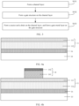
- FIG. 3 is a schematic flowchart of a method for preparing the field effect transistor according to an embodiment of this application. The method includes the following steps.
- Step S101 Form a channel layer.
- a buffer layer 16 may be first formed on a substrate 10, and a GaN layer 112 and an AlGaN barrier layer 111 are sequentially formed on the buffer layer 16; and the GaN layer 112 and the AlGaN barrier layer 111 form a channel layer 11, thereby forming a structure shown in FIG. 4a .
- the buffer layer 16, the GaN layer 112, and the AlGaN barrier layer 111 may be sequentially staked on the substrate 10 by using a process such as epitaxial growth or deposition.
- Step S102 Form a gate structure on the channel layer.
- a pGaN layer 141 and an nGaN layer 142 are sequentially formed on the AlGaN barrier layer 111, the pGaN layer 141 and the nGaN layer 142 are etched, and a part of the pGaN layer 141 and a part of the nGaN layer 142 are kept to form a gate structure 14, thereby forming a structure shown in FIG. 4b .
- the pGaN layer 141 and the nGaN layer 142 may be sequentially stacked on the AlGaN barrier layer 111 by using a process such as epitaxial growth or deposition.
- a doping element of the pGaN layer 141 may be magnesium (Mg), a doping density of the pGaN layer 141 is controlled between 1 ⁇ 10 18 cm -3 and 1 ⁇ 10 19 cm -3 , a thickness of the pGaN layer 141 may be controlled between 50 nm and 70 nm, a doping element of the nGaN layer 142 may be silicon (Si), germanium (Ge), or the like, a doping density of the nGaN layer 142 may be controlled between 1 ⁇ 10 16 cm -3 and 5 ⁇ 10 19 cm -3 , and a thickness of the nGaN layer 142 may be less than or equal to 40 nm.
- Mg magnesium
- a doping density of the pGaN layer 141 is controlled between 1 ⁇ 10 18 cm -3 and 1 ⁇ 10 19 cm -3
- a thickness of the pGaN layer 141 may be controlled between 50 nm and 70 nm
- doping densities and thicknesses of the pGaN layer 141 and the nGaN layer 142 are adjusted and controlled, so that a charge storage effect during operation of a device can be reduced, carriers in the pGaN layer 141 are exhausted as much as possible, and redundant-charge storage is avoided, thereby improving operating threshold voltage stability of the device.
- Step S103 Form a source and a drain on the channel layer, and form a gate metal layer on the gate structure.
- a metal layer may be formed by using a process such as deposition, and then the metal layer is etched to form the source 12, the drain 13, and a gate metal layer 15; and the source 12 and the drain 13 are located on the AlGaN barrier layer 111, and the gate metal layer 15 is located on the nGaN layer 142 and is in ohmic contact with the nGaN layer 142, to form a structure shown in FIG. 4c .
- An nGaN/pGaN reverse bias diode is used to replace a gate metal/pGaN Schottky diode in a current technology to withstand a voltage, so that a gate voltage-withstand capability of the field effect transistor can be greatly increased, thereby improving a breakdown capability of the field effect transistor.
- the gate metal layer 15 is in ohmic contact with the nGaN layer 142. Forming ohmic contact between metal and a semiconductor means that a pure resistor is at a contact point, and smaller resistance is better, so that when a component is operated, most voltages are applied to an active area instead of a contact surface. In addition, the ohmic contact does not involve long-term thermo-electron bombardment, and is highly reliable.
- the gate metal layer is in ohmic contact with the gate structure, so that reliability of a connection between the gate metal layer and the gate structure can be improved, thereby improving reliability of the field effect transistor.
- the method may further include the following step.
- Step S104 Form a passivation layer.
- a passivation layer 17 covers the gate structure 14 and the AlGaN barrier layer 111 that is exposed, and the passivation layer 17 is etched to form a source contact hole V1, a drain contact hole V2, and a gate contact hole V3.
- the source 12 formed in step S103 is in contact with the AlGaN barrier layer 111 by using the source contact hole V1
- the drain 13 is in contact with the AlGaN barrier layer 111 by using the drain contact hole V2
- the gate metal layer 15 is in contact with the nGaN layer 142 by using the gate contact hole V3, to form the field effect transistor shown in FIG. 2 .
- a gate voltage-withstand capability of the field effect transistor can be greatly increased by replacing a gate metal/pGaN Schottky diode in a current technology with an nGaN/pGaN reverse bias diode, thereby improving a breakdown capability of the field effect transistor.
- the gate metal layer is in ohmic contact with the gate structure, so that reliability of a connection between the gate metal layer and the gate structure can be improved, thereby improving reliability of the field effect transistor.
- Doping densities and thicknesses of the pGaN layer and the nGaN layer are adjusted and controlled, so that a charge storage effect during operation of a device can be reduced, carriers in the pGaN layer are exhausted as much as possible, and redundant-charge storage is avoided, thereby improving operating threshold voltage stability of the device.
- An embodiment of this application further provides a switch circuit.
- the switch circuit may be an AC-DC conversion circuit, a high-voltage conversion circuit, or a switch circuit in a half-bridge rectifier circuit.
- the switch circuit includes a mainboard and any one of the foregoing field effect transistors provided in embodiments of this application, where the field effect transistor is disposed on the mainboard.
- a problem-resolving principle of the switch circuit is similar to that of one of the foregoing field effect transistors. Therefore, for implementation of the switch circuit, refer to the implementation of the foregoing field effect transistors. Repeated content is not described again.
Landscapes
- Junction Field-Effect Transistors (AREA)
Applications Claiming Priority (2)
| Application Number | Priority Date | Filing Date | Title |
|---|---|---|---|
| CN202110256517.7A CN113178475A (zh) | 2021-03-09 | 2021-03-09 | 一种场效应管、其制备方法及开关电路 |
| PCT/CN2022/079143 WO2022188694A1 (zh) | 2021-03-09 | 2022-03-03 | 一种场效应管、其制备方法及开关电路 |
Publications (2)
| Publication Number | Publication Date |
|---|---|
| EP4300587A1 true EP4300587A1 (de) | 2024-01-03 |
| EP4300587A4 EP4300587A4 (de) | 2024-08-28 |
Family
ID=76921853
Family Applications (1)
| Application Number | Title | Priority Date | Filing Date |
|---|---|---|---|
| EP22766220.2A Pending EP4300587A4 (de) | 2021-03-09 | 2022-03-03 | Feldeffekttransistor, herstellungsverfahren dafür und schaltkreis |
Country Status (4)
| Country | Link |
|---|---|
| US (1) | US20230420537A1 (de) |
| EP (1) | EP4300587A4 (de) |
| CN (1) | CN113178475A (de) |
| WO (1) | WO2022188694A1 (de) |
Families Citing this family (8)
| Publication number | Priority date | Publication date | Assignee | Title |
|---|---|---|---|---|
| CN113178475A (zh) * | 2021-03-09 | 2021-07-27 | 华为技术有限公司 | 一种场效应管、其制备方法及开关电路 |
| CN113871479A (zh) * | 2021-09-07 | 2021-12-31 | 南方科技大学 | 晶体管结构及其制备方法 |
| CN113838675A (zh) * | 2021-09-22 | 2021-12-24 | 湖南师范大学 | 柔性与门逻辑器件及其制作方法 |
| CN114400246A (zh) * | 2021-12-13 | 2022-04-26 | 晶通半导体(深圳)有限公司 | 反向导通高迁移率晶体管 |
| CN115458595A (zh) * | 2022-08-30 | 2022-12-09 | 西安电子科技大学 | 氧化镓氮化镓异质结栅的氮化镓hemt器件及制备方法 |
| CN115425078A (zh) * | 2022-11-03 | 2022-12-02 | 江苏长晶科技股份有限公司 | 一种hemt器件及其制备方法 |
| CN119008686A (zh) * | 2024-08-15 | 2024-11-22 | 英诺赛科(苏州)半导体有限公司 | 一种功率器件及其制备方法 |
| CN121442733B (zh) * | 2025-12-31 | 2026-03-27 | 广东工业大学 | 一种基于ii型异质结栅结构的氮化镓晶体管 |
Family Cites Families (9)
| Publication number | Priority date | Publication date | Assignee | Title |
|---|---|---|---|---|
| JP5114947B2 (ja) * | 2006-12-28 | 2013-01-09 | 富士通株式会社 | 窒化物半導体装置とその製造方法 |
| US8895993B2 (en) * | 2011-01-31 | 2014-11-25 | Taiwan Semiconductor Manufacturing Company, Ltd. | Low gate-leakage structure and method for gallium nitride enhancement mode transistor |
| US20130062614A1 (en) * | 2011-09-09 | 2013-03-14 | Texas Instruments Incorporated | Group iii-v enhancement mode transistor with thyristor gate |
| JP6161246B2 (ja) * | 2012-09-28 | 2017-07-12 | トランスフォーム・ジャパン株式会社 | 半導体装置及び半導体装置の製造方法 |
| US8866192B1 (en) * | 2013-07-17 | 2014-10-21 | Taiwan Semiconductor Manufacturing Company, Ltd. | Semiconductor device, high electron mobility transistor (HEMT) and method of manufacturing |
| US10014402B1 (en) * | 2016-12-14 | 2018-07-03 | Taiwan Semiconductor Manufacturing Co., Ltd. | High electron mobility transistor (HEMT) device structure |
| CN107680998A (zh) * | 2017-10-24 | 2018-02-09 | 江苏华功半导体有限公司 | 一种GaN基p型栅HFET器件及其制备方法 |
| CN109888002A (zh) * | 2019-02-22 | 2019-06-14 | 南方科技大学 | 具有超级结栅结构的常关型氮化镓场效应管及其制造方法 |
| CN113178475A (zh) * | 2021-03-09 | 2021-07-27 | 华为技术有限公司 | 一种场效应管、其制备方法及开关电路 |
-
2021
- 2021-03-09 CN CN202110256517.7A patent/CN113178475A/zh active Pending
-
2022
- 2022-03-03 EP EP22766220.2A patent/EP4300587A4/de active Pending
- 2022-03-03 WO PCT/CN2022/079143 patent/WO2022188694A1/zh not_active Ceased
-
2023
- 2023-09-08 US US18/463,417 patent/US20230420537A1/en active Pending
Also Published As
| Publication number | Publication date |
|---|---|
| WO2022188694A1 (zh) | 2022-09-15 |
| US20230420537A1 (en) | 2023-12-28 |
| EP4300587A4 (de) | 2024-08-28 |
| CN113178475A (zh) | 2021-07-27 |
Similar Documents
| Publication | Publication Date | Title |
|---|---|---|
| EP4300587A1 (de) | Feldeffekttransistor, herstellungsverfahren dafür und schaltkreis | |
| KR101562879B1 (ko) | 반도체 장치 | |
| US8552471B2 (en) | Semiconductor apparatus having reverse blocking characteristics and method of manufacturing the same | |
| JP5281748B2 (ja) | Iii族窒化物素子の不動態化およびその方法 | |
| US20130087803A1 (en) | Monolithically integrated hemt and schottky diode | |
| US7884395B2 (en) | Semiconductor apparatus | |
| US9087704B2 (en) | Semiconductor devices and methods of manufacturing the semiconductor device | |
| US20130240951A1 (en) | Gallium nitride superjunction devices | |
| JP2005203753A (ja) | トレンチ構造を有するiii族窒化物半導体装置 | |
| JP2014212316A (ja) | ショットキーダイオードおよび高電子移動度トランジスタを備えた半導体デバイスの製造方法 | |
| CN1957474A (zh) | Ⅲ-氮电流控制装置及其制造方法 | |
| US20230187523A1 (en) | Hybrid gate field effect transistor, method for preparing hybrid gate field effect transistor, and switch circuit | |
| US20170033098A1 (en) | GaN-BASED SCHOTTKY DIODE RECTIFIER | |
| JP6679036B1 (ja) | ダイオード、ダイオードの製造方法および電気機器 | |
| CN104952938A (zh) | 一种氮化镓异质结mis栅控功率二极管及其制造方法 | |
| TW202141789A (zh) | 三五族半導體裝置 | |
| CN112310208A (zh) | 增强型氮化镓基晶体管及其制备方法、电子装置 | |
| JP2010165896A (ja) | 半導体装置及びその製造方法 | |
| CN109192788A (zh) | 一种基于场板和复合势垒层的GaN基肖特基势垒二极管 | |
| CN116314316B (zh) | 一种抗反向导通电流的凹栅增强型GaN HEMT及制作方法 | |
| US12136675B2 (en) | Enhancement-mode device and preparation method therefor | |
| CN116529892B (zh) | 一种肖特基二极管 | |
| EP3324440A1 (de) | Vorrichtung mit niedrigem widerstand und niedriger leckage | |
| CN220065708U (zh) | 一种具有复合栅结构的功率器件 | |
| CN118016665B (zh) | 集成SBD的SiC衬底上增强型GaN HEMT器件 |
Legal Events
| Date | Code | Title | Description |
|---|---|---|---|
| STAA | Information on the status of an ep patent application or granted ep patent |
Free format text: STATUS: THE INTERNATIONAL PUBLICATION HAS BEEN MADE |
|
| PUAI | Public reference made under article 153(3) epc to a published international application that has entered the european phase |
Free format text: ORIGINAL CODE: 0009012 |
|
| STAA | Information on the status of an ep patent application or granted ep patent |
Free format text: STATUS: REQUEST FOR EXAMINATION WAS MADE |
|
| 17P | Request for examination filed |
Effective date: 20230926 |
|
| AK | Designated contracting states |
Kind code of ref document: A1 Designated state(s): AL AT BE BG CH CY CZ DE DK EE ES FI FR GB GR HR HU IE IS IT LI LT LU LV MC MK MT NL NO PL PT RO RS SE SI SK SM TR |
|
| DAV | Request for validation of the european patent (deleted) | ||
| DAX | Request for extension of the european patent (deleted) | ||
| REG | Reference to a national code |
Ref country code: DE Ref legal event code: R079 Free format text: PREVIOUS MAIN CLASS: H01L0029060000 Ipc: H01L0029778000 |
|
| A4 | Supplementary search report drawn up and despatched |
Effective date: 20240725 |
|
| RIC1 | Information provided on ipc code assigned before grant |
Ipc: H01L 29/20 20060101ALN20240719BHEP Ipc: H01L 23/31 20060101ALN20240719BHEP Ipc: H01L 29/10 20060101ALN20240719BHEP Ipc: H01L 21/337 20060101ALI20240719BHEP Ipc: H01L 29/778 20060101AFI20240719BHEP |