EP4307352B1 - Gehäusestruktur, dafür vorgesehenes herstellungsverfahren und halbleiterbauelement - Google Patents
Gehäusestruktur, dafür vorgesehenes herstellungsverfahren und halbleiterbauelement Download PDFInfo
- Publication number
- EP4307352B1 EP4307352B1 EP22836031.9A EP22836031A EP4307352B1 EP 4307352 B1 EP4307352 B1 EP 4307352B1 EP 22836031 A EP22836031 A EP 22836031A EP 4307352 B1 EP4307352 B1 EP 4307352B1
- Authority
- EP
- European Patent Office
- Prior art keywords
- pads
- pad
- layer
- redistribution layers
- redistribution
- Prior art date
- Legal status (The legal status is an assumption and is not a legal conclusion. Google has not performed a legal analysis and makes no representation as to the accuracy of the status listed.)
- Active
Links
Images




Classifications
-
- H—ELECTRICITY
- H10—SEMICONDUCTOR DEVICES; ELECTRIC SOLID-STATE DEVICES NOT OTHERWISE PROVIDED FOR
- H10W—GENERIC PACKAGES, INTERCONNECTIONS, CONNECTORS OR OTHER CONSTRUCTIONAL DETAILS OF DEVICES COVERED BY CLASS H10
- H10W20/00—Interconnections in chips, wafers or substrates
- H10W20/40—Interconnections external to wafers or substrates, e.g. back-end-of-line [BEOL] metallisations or vias connecting to gate electrodes
- H10W20/41—Interconnections external to wafers or substrates, e.g. back-end-of-line [BEOL] metallisations or vias connecting to gate electrodes characterised by their conductive parts
- H10W20/42—Vias, e.g. via plugs
-
- H—ELECTRICITY
- H10—SEMICONDUCTOR DEVICES; ELECTRIC SOLID-STATE DEVICES NOT OTHERWISE PROVIDED FOR
- H10P—GENERIC PROCESSES OR APPARATUS FOR THE MANUFACTURE OR TREATMENT OF DEVICES COVERED BY CLASS H10
- H10P74/00—Testing or measuring during manufacture or treatment of wafers, substrates or devices
- H10P74/27—Structural arrangements therefor
- H10P74/273—Interconnections for measuring or testing, e.g. probe pads
-
- H—ELECTRICITY
- H10—SEMICONDUCTOR DEVICES; ELECTRIC SOLID-STATE DEVICES NOT OTHERWISE PROVIDED FOR
- H10P—GENERIC PROCESSES OR APPARATUS FOR THE MANUFACTURE OR TREATMENT OF DEVICES COVERED BY CLASS H10
- H10P74/00—Testing or measuring during manufacture or treatment of wafers, substrates or devices
- H10P74/20—Testing or measuring during manufacture or treatment of wafers, substrates or devices characterised by the properties tested or measured, e.g. structural or electrical properties
- H10P74/203—Structural properties, e.g. testing or measuring thicknesses, line widths, warpage, bond strengths or physical defects
-
- H—ELECTRICITY
- H10—SEMICONDUCTOR DEVICES; ELECTRIC SOLID-STATE DEVICES NOT OTHERWISE PROVIDED FOR
- H10P—GENERIC PROCESSES OR APPARATUS FOR THE MANUFACTURE OR TREATMENT OF DEVICES COVERED BY CLASS H10
- H10P74/00—Testing or measuring during manufacture or treatment of wafers, substrates or devices
- H10P74/27—Structural arrangements therefor
- H10P74/277—Circuits for electrically characterising or monitoring manufacturing processes, e.g. circuits in tested chips or circuits in testing wafers
-
- H—ELECTRICITY
- H10—SEMICONDUCTOR DEVICES; ELECTRIC SOLID-STATE DEVICES NOT OTHERWISE PROVIDED FOR
- H10W—GENERIC PACKAGES, INTERCONNECTIONS, CONNECTORS OR OTHER CONSTRUCTIONAL DETAILS OF DEVICES COVERED BY CLASS H10
- H10W20/00—Interconnections in chips, wafers or substrates
- H10W20/40—Interconnections external to wafers or substrates, e.g. back-end-of-line [BEOL] metallisations or vias connecting to gate electrodes
- H10W20/41—Interconnections external to wafers or substrates, e.g. back-end-of-line [BEOL] metallisations or vias connecting to gate electrodes characterised by their conductive parts
- H10W20/435—Cross-sectional shapes or dispositions of interconnections
-
- H—ELECTRICITY
- H10—SEMICONDUCTOR DEVICES; ELECTRIC SOLID-STATE DEVICES NOT OTHERWISE PROVIDED FOR
- H10W—GENERIC PACKAGES, INTERCONNECTIONS, CONNECTORS OR OTHER CONSTRUCTIONAL DETAILS OF DEVICES COVERED BY CLASS H10
- H10W46/00—Marks applied to devices, e.g. for alignment or identification
-
- H—ELECTRICITY
- H10—SEMICONDUCTOR DEVICES; ELECTRIC SOLID-STATE DEVICES NOT OTHERWISE PROVIDED FOR
- H10W—GENERIC PACKAGES, INTERCONNECTIONS, CONNECTORS OR OTHER CONSTRUCTIONAL DETAILS OF DEVICES COVERED BY CLASS H10
- H10W70/00—Package substrates; Interposers; Redistribution layers [RDL]
- H10W70/60—Insulating or insulated package substrates; Interposers; Redistribution layers
-
- H—ELECTRICITY
- H10—SEMICONDUCTOR DEVICES; ELECTRIC SOLID-STATE DEVICES NOT OTHERWISE PROVIDED FOR
- H10W—GENERIC PACKAGES, INTERCONNECTIONS, CONNECTORS OR OTHER CONSTRUCTIONAL DETAILS OF DEVICES COVERED BY CLASS H10
- H10W70/00—Package substrates; Interposers; Redistribution layers [RDL]
- H10W70/60—Insulating or insulated package substrates; Interposers; Redistribution layers
- H10W70/62—Insulating or insulated package substrates; Interposers; Redistribution layers characterised by their interconnections
- H10W70/65—Shapes or dispositions of interconnections
-
- H—ELECTRICITY
- H10—SEMICONDUCTOR DEVICES; ELECTRIC SOLID-STATE DEVICES NOT OTHERWISE PROVIDED FOR
- H10W—GENERIC PACKAGES, INTERCONNECTIONS, CONNECTORS OR OTHER CONSTRUCTIONAL DETAILS OF DEVICES COVERED BY CLASS H10
- H10W70/00—Package substrates; Interposers; Redistribution layers [RDL]
- H10W70/60—Insulating or insulated package substrates; Interposers; Redistribution layers
- H10W70/62—Insulating or insulated package substrates; Interposers; Redistribution layers characterised by their interconnections
- H10W70/65—Shapes or dispositions of interconnections
- H10W70/652—Cross-sectional shapes
-
- H—ELECTRICITY
- H10—SEMICONDUCTOR DEVICES; ELECTRIC SOLID-STATE DEVICES NOT OTHERWISE PROVIDED FOR
- H10W—GENERIC PACKAGES, INTERCONNECTIONS, CONNECTORS OR OTHER CONSTRUCTIONAL DETAILS OF DEVICES COVERED BY CLASS H10
- H10W72/00—Interconnections or connectors in packages
- H10W72/90—Bond pads, in general
-
- H—ELECTRICITY
- H10—SEMICONDUCTOR DEVICES; ELECTRIC SOLID-STATE DEVICES NOT OTHERWISE PROVIDED FOR
- H10W—GENERIC PACKAGES, INTERCONNECTIONS, CONNECTORS OR OTHER CONSTRUCTIONAL DETAILS OF DEVICES COVERED BY CLASS H10
- H10W90/00—Package configurations
-
- H—ELECTRICITY
- H10—SEMICONDUCTOR DEVICES; ELECTRIC SOLID-STATE DEVICES NOT OTHERWISE PROVIDED FOR
- H10W—GENERIC PACKAGES, INTERCONNECTIONS, CONNECTORS OR OTHER CONSTRUCTIONAL DETAILS OF DEVICES COVERED BY CLASS H10
- H10W90/00—Package configurations
- H10W90/701—Package configurations characterised by the relative positions of pads or connectors relative to package parts
- H10W90/751—Package configurations characterised by the relative positions of pads or connectors relative to package parts of bond wires
- H10W90/754—Package configurations characterised by the relative positions of pads or connectors relative to package parts of bond wires between a chip and a stacked insulating package substrate, interposer or RDL
-
- H—ELECTRICITY
- H10—SEMICONDUCTOR DEVICES; ELECTRIC SOLID-STATE DEVICES NOT OTHERWISE PROVIDED FOR
- H10W—GENERIC PACKAGES, INTERCONNECTIONS, CONNECTORS OR OTHER CONSTRUCTIONAL DETAILS OF DEVICES COVERED BY CLASS H10
- H10W70/00—Package substrates; Interposers; Redistribution layers [RDL]
- H10W70/01—Manufacture or treatment
- H10W70/05—Manufacture or treatment of insulating or insulated package substrates, or of interposers, or of redistribution layers
-
- H—ELECTRICITY
- H10—SEMICONDUCTOR DEVICES; ELECTRIC SOLID-STATE DEVICES NOT OTHERWISE PROVIDED FOR
- H10W—GENERIC PACKAGES, INTERCONNECTIONS, CONNECTORS OR OTHER CONSTRUCTIONAL DETAILS OF DEVICES COVERED BY CLASS H10
- H10W72/00—Interconnections or connectors in packages
- H10W72/01—Manufacture or treatment
- H10W72/019—Manufacture or treatment of bond pads
-
- H—ELECTRICITY
- H10—SEMICONDUCTOR DEVICES; ELECTRIC SOLID-STATE DEVICES NOT OTHERWISE PROVIDED FOR
- H10W—GENERIC PACKAGES, INTERCONNECTIONS, CONNECTORS OR OTHER CONSTRUCTIONAL DETAILS OF DEVICES COVERED BY CLASS H10
- H10W72/00—Interconnections or connectors in packages
- H10W72/01—Manufacture or treatment
- H10W72/019—Manufacture or treatment of bond pads
- H10W72/01931—Manufacture or treatment of bond pads using blanket deposition
- H10W72/01933—Manufacture or treatment of bond pads using blanket deposition in liquid form, e.g. spin coating, spray coating or immersion coating
- H10W72/01935—Manufacture or treatment of bond pads using blanket deposition in liquid form, e.g. spin coating, spray coating or immersion coating by plating, e.g. electroless plating or electroplating
-
- H—ELECTRICITY
- H10—SEMICONDUCTOR DEVICES; ELECTRIC SOLID-STATE DEVICES NOT OTHERWISE PROVIDED FOR
- H10W—GENERIC PACKAGES, INTERCONNECTIONS, CONNECTORS OR OTHER CONSTRUCTIONAL DETAILS OF DEVICES COVERED BY CLASS H10
- H10W72/00—Interconnections or connectors in packages
- H10W72/50—Bond wires
- H10W72/59—Bond pads specially adapted therefor
-
- H—ELECTRICITY
- H10—SEMICONDUCTOR DEVICES; ELECTRIC SOLID-STATE DEVICES NOT OTHERWISE PROVIDED FOR
- H10W—GENERIC PACKAGES, INTERCONNECTIONS, CONNECTORS OR OTHER CONSTRUCTIONAL DETAILS OF DEVICES COVERED BY CLASS H10
- H10W72/00—Interconnections or connectors in packages
- H10W72/90—Bond pads, in general
- H10W72/921—Structures or relative sizes of bond pads
- H10W72/922—Bond pads being integral with underlying chip-level interconnections
-
- H—ELECTRICITY
- H10—SEMICONDUCTOR DEVICES; ELECTRIC SOLID-STATE DEVICES NOT OTHERWISE PROVIDED FOR
- H10W—GENERIC PACKAGES, INTERCONNECTIONS, CONNECTORS OR OTHER CONSTRUCTIONAL DETAILS OF DEVICES COVERED BY CLASS H10
- H10W72/00—Interconnections or connectors in packages
- H10W72/90—Bond pads, in general
- H10W72/921—Structures or relative sizes of bond pads
- H10W72/926—Multiple bond pads having different sizes
-
- H—ELECTRICITY
- H10—SEMICONDUCTOR DEVICES; ELECTRIC SOLID-STATE DEVICES NOT OTHERWISE PROVIDED FOR
- H10W—GENERIC PACKAGES, INTERCONNECTIONS, CONNECTORS OR OTHER CONSTRUCTIONAL DETAILS OF DEVICES COVERED BY CLASS H10
- H10W72/00—Interconnections or connectors in packages
- H10W72/90—Bond pads, in general
- H10W72/941—Dispositions of bond pads
- H10W72/9415—Dispositions of bond pads relative to the surface, e.g. recessed, protruding
-
- H—ELECTRICITY
- H10—SEMICONDUCTOR DEVICES; ELECTRIC SOLID-STATE DEVICES NOT OTHERWISE PROVIDED FOR
- H10W—GENERIC PACKAGES, INTERCONNECTIONS, CONNECTORS OR OTHER CONSTRUCTIONAL DETAILS OF DEVICES COVERED BY CLASS H10
- H10W72/00—Interconnections or connectors in packages
- H10W72/90—Bond pads, in general
- H10W72/941—Dispositions of bond pads
- H10W72/944—Dispositions of multiple bond pads
- H10W72/9445—Top-view layouts, e.g. mirror arrays
-
- H—ELECTRICITY
- H10—SEMICONDUCTOR DEVICES; ELECTRIC SOLID-STATE DEVICES NOT OTHERWISE PROVIDED FOR
- H10W—GENERIC PACKAGES, INTERCONNECTIONS, CONNECTORS OR OTHER CONSTRUCTIONAL DETAILS OF DEVICES COVERED BY CLASS H10
- H10W72/00—Interconnections or connectors in packages
- H10W72/90—Bond pads, in general
- H10W72/951—Materials of bond pads
- H10W72/952—Materials of bond pads comprising metals or metalloids, e.g. PbSn, Ag or Cu
-
- H—ELECTRICITY
- H10—SEMICONDUCTOR DEVICES; ELECTRIC SOLID-STATE DEVICES NOT OTHERWISE PROVIDED FOR
- H10W—GENERIC PACKAGES, INTERCONNECTIONS, CONNECTORS OR OTHER CONSTRUCTIONAL DETAILS OF DEVICES COVERED BY CLASS H10
- H10W72/00—Interconnections or connectors in packages
- H10W72/90—Bond pads, in general
- H10W72/961—Functions of bonds pads
- H10W72/967—Multiple bond pads having different functions
Definitions
- the invention relates to the technical field of semiconductors, in particular to a package structure, a method for manufacturing the same and a semiconductor device.
- US 2007/090356 A1 discloses a semiconductor device, including: a semiconductor substrate having an electrode; a resin layer provided on the surface of the semiconductor substrate on which the electrode is formed and having a concave portion formed on a second surface on the other side of a first surface facing the semiconductor substrate; a test pad electrically connected to the electrode and formed inside the concave portion; wiring electrically connected to the test pad, going through on the second surface of the resin layer, and narrower in width than the test pad; and a land electrically connected to the test pad and having an external terminal formed thereon.
- US 2002/180026 A1 discloses a semiconductor wafer designed to avoid probed marks while testing, the semiconductor wafer designed to avoid probed marks while testing includes: a plurality of semiconductor chips, each chip having an integrated circuit forming surface formed on the same plane of the semiconductor wafer, wherein the chip has a plurality of bonding pads on the integrated circuit forming surface; a plurality of cutting paths, each cutting path being formed between two adjoining chips; a plurality of metal interconnects being on the integrated circuit forming surface of the chip and electrically connecting with the corresponding bonding pad respectively; a passivation layer covering the plurality of the metal interconnects and having a plurality of the first openings and the second openings; a plurality of test pads located at the first openings of the passivation layer and connecting to the corresponding bonding pad through a corresponding metal interconnect; and a plurality of contact pads being located at the second opening of the passivation layer, wherein the contact pad is connected in series with corresponding metal interconnect between the corresponding bonding pad and test pad
- embodiments of the disclosure provides a package structure, a method for manufacturing the same, and a semiconductor device.
- the present disclosure provides a package structure, a manufacturing method therefor and a semiconductor device as defined in the appended claims 1-13.
- N first pads are provided in a top metal layer to perform a test on the semiconductor functional structure at a first operating speed. Some first pads are arranged side by side along a first direction near a first edge of the semiconductor functional structure. Other first pads are arranged side by side along the first direction near a second edge of the semiconductor functional structure.
- the second pads corresponding to the first pads one by on are provided in the redistribution layers on the first pads to perform a test on the semiconductor functional structure at a second operating speed.
- a relative position between the second pad and the third pad for some redistribution layers is different from a relative position between the second pad and the third pad for other redistribution layers.
- a center point of the second pad is offset in a same direction and is offset by an equal distance relative to a center point of a corresponding first pad for all the second pads; by doing so, the N first pads and the N second pads keep a same relative position. Meanwhile, relative positions between the second pads and the third pads located at different edges are different; by doing so, the redistribution layers located at the two edges can keep a large fault tolerance rate, and can all be close to the edges but not beyond the edges. Therefore, the first pads and the second pads are ensured to be in favorable positions which are beneficial to saving a total area, and meanwhile, a same set of probe cards may be used for tests at the two different operating speeds. Compared with using two sets of probe cards to test separately, test cost and time are saved, and production cycle and manufacturing cost are reduced.
- a term “A is connected to B” includes a case where A and B are in direct contact, or a case where A and B are in indirect contact through an intermediate conductive structure.
- Terms “first”, “second”, and so on are used to distinguish similar objects and need not be used to describe a particular order or priority.
- a term "layer” refers to a portion of an object that includes a region having a thickness.
- the layer may extend on a lower surface or an upper surface of the structure, and its area may be less than or equal to an area of the extended surface on which the layer lies. It is to be noted that the technical solution described in the embodiments of this disclosure can be arbitrarily combined without conflict.
- a semiconductor functional structure involved in the embodiments of the disclosure is a part that will be used in a subsequent manufacturing process to form a final semiconductor device, and is a core part to realize main functions of the semiconductor device.
- the final semiconductor device may include, but is not limited to, a memory.
- a package structure of a semiconductor device such as a DRAM (Dynamic Random Access Memory)
- DRAM Dynamic Random Access Memory
- RDL Redistribution Layer
- Windowing on redistribution layers means that a redistribution layers are formed on the top metal layer of the semiconductor functional structure.
- a passivation layer or an insulating layer is formed on the redistribution layers, and then windowing regions are formed on the passivation layer or the insulating layer, so as to expose parts of each of the redistribution layers and form two pads arranged side by side.
- One of the two pads is used for carrying out the punch needles test of probe card, and the other is used for leading out the bonding wires on the pads.
- the redistribution layers may play a role in adjusting positions of the pads in the semiconductor device, and may also play a role in strengthening power supply network of power ground.
- the top metal layer is relatively thin, and there is a gasket structure below.
- a material of the redistribution layer is a metal.
- the redistribution layer is thicker than the top metal layer, and deep and rough marks will be resulted by a probe card test. The marks will affect the yield of the wire bond package. Therefore, in the redistribution layer, the pad for testing and is required to be distinguished from the pad for leading out bonding wires. No matter which of the above windowing modes is adopted in the package structure, there is no great influence on the function of the semiconductor device. Redistribution layer windowing is beneficial to improve performance, but the production cycle and production cost are increased.
- one of the above two windowing modes is selected to design a package structure according to an actual need of semiconductor device.
- the package structure includes the mode of windowing on a top metal and the mode of windowing on redistribution layers.
- a first type pad 102 is arranged in a top metal layer 101.
- the first type pad 102 may be used to perform a test at a low speed and lead out a bonding wire.
- the second type pad 104 is used to perform a test at a high speed
- the third type pad 105 is used to lead out a bonding wire.
- a probe card for the test needs to hit center points of all the first type pads 102.
- the probe card for the test needs to hit center points of all the second type pads 104.
- FIG. 1 it can be seen from FIG. 1 that the first type pad 102 and the second pad 104 are in different layers of the package structure and that relative positions of the first type pad 102 and the second pad 104 in the different layers are different.
- the redistribution layers 103 are also required to be provided at the opposite two edges of the semiconductor functional structure.
- an area occupied by the second type pad 104 and the third type pad 105 together is larger than an area occupied by the first type pad 102, a redistribution layer103 at a position of at least one of the edges is prone to extend beyond the edge.
- the embodiments of the disclosure provide a package structure, a method for manufacturing the same and a semiconductor device.
- the package structure includes: an isolation layer having a plurality of via holes, N first pads, N redistribution layers, a first insulating layer, second pads and third pads.
- the isolation layer covers a surface of an interconnect layer.
- the via holes expose parts of the interconnect layer, and the top surface of the interconnect layer serves as the top surface of the semiconductor functional structure.
- Each of the N first pads is formed by the interconnect layer exposed by a corresponding via hole.
- the N is a positive integer greater than 1.
- Each of the N redistribution layers covers the isolation layer and is electrically connected with a corresponding one of the N first pads.
- first pads are arranged side by side along a first direction near a first edge of the semiconductor functional structure. Some other first pads are arranged side by side along the first direction near a second edge of the semiconductor functional structure. The first edge and the second edge are two opposite edges of the semiconductor functional structure.
- the first insulating layer covers and exposes parts of each of the redistribution layers. The exposed parts of each of the redistribution layers form a second pad and a third pad. Both an offset direction and an offset distance between a center point of a second pad and a center point of a corresponding first pad are same for all the second pads.
- a relative position between a second pad and a third pad for some the redistribution layers is different from a relative position between a second pad and a third pad in other redistribution layers.
- the first pads and the second pads are used for testing the semiconductor functional structure at different operating speeds.
- the third pads are used for performing functional interaction corresponding to a content tested by the second pads.
- the first direction referred to in the embodiments of the disclosure is parallel to the surface of the semiconductor functional structure
- the second direction referred to in the embodiments of the disclosure is parallel to the semiconductor functional structure and perpendicular to the first direction
- a third direction referred to in the embodiments of the disclosure is perpendicular to both the first direction and the second direction.
- the first direction may be parallel to the X-axis direction
- the second direction may be parallel to the Y-axis direction
- the third direction may be parallel to the Z-axis direction.
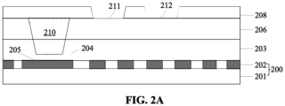
- the package structure includes a substrate (not shown in FIG. 2A ).
- a material for forming the substrate may include silicon (Si), germanium (Ge), silicon germanium (SiGe), silicon on insulator (SOI), or germanium on insulator (GOI).
- a semiconductor functional structure 200 is located on the substrate.
- the semiconductor functional structure 200 includes a semiconductor functional layer 201 and a interconnect layer 202 located on a surface of the semiconductor functional layer 201.
- the interconnect layer 202 is used to lead out electrical signals of the functional structures in the semiconductor functional layer 201 to make the functional structures work.
- the interconnect layer 202 includes a top metal layer, not only for leading out the electrical signals from the functional structure but also for supporting the semiconductor functional structure 200.
- FIG. 2A is a cross-sectional view where part of the interconnect layer 202 has been removed.
- parts in the interconnect layer are not truncated, but interconnected, that is, the parts in the interconnect layer may be continuous on other sections.
- An isolation layer 203 covers a surface of the interconnect layer 202, and is configured for isolating the interconnect layer 202 and the subsequently formed redistribution layer 206 in part of a region.
- a via hole 204 is provided in the isolation layer 203, and the via hole 204 exposes part of the interconnect layer 202.
- a shape of the via hole 204 may be cylindrical or inverted trapezoidal or any suitable shape.
- a material for forming the isolation layer 203 includes, but is not limited to, tetraethyl orthosilicate (TEOS).
- a first pad 205 is formed by the interconnect layer 202 exposed by one of the via holes 204.
- a plurality of via holes 204 are included within the isolation layer 203, such that a plurality of first pads 205 are formed by the exposure of the plurality of via holes 204.
- the first pads 205 are used for a first type test.
- the first pads 205 can also be used to achieve functional interaction corresponding to a content of the first type test.
- the first type test may be understood as some tests performed on the semiconductor functional structure at a lower operating speed. It is to be noted that, in a memory, an operating speed refers to a read-write speed of the memory.
- the achievement of the functional interaction corresponding to the content of the first type test may be understood as leading out bonding wires on the first pads. That is, when performing the first type test, the first pads 205 can be used to contact a probe card, and a plurality of probes in the probe card correspond to the N first pads one by one, so as to realize electrical connections between the interconnect layer and other test systems.
- the first pads 205 are arranged at two opposite edges of the semiconductor functional structure.
- the N first pads are divided into two parts, namely first part of the first pads 2051 and second part of the first pads 2052.
- the first part of the first pads 2051 includes M1 first pads, and the M1 first pads are arranged side by side along the first direction near a first edge 20a of the semiconductor functional structure.
- the second part of the first pads 2052 includes M2 first pads, and the M2 first pads are arranged side by side along the first direction near a second edge 20b of the semiconductor functional structure.
- the first edge 20a and the second edge 20b are two opposite edges of the semiconductor functional structure.
- M1+M2 N.
- FIG. 2A is a partial cross-sectional schematic diagram of a package structure where the first pad 205 is in direct contact with a redistribution layer 206.
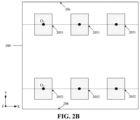
- FIG. 2B is a top view of an example of a package structure, in which other layers are omitted in order to show a position arrangement of the first pads more clearly in FIG. 2B .
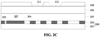
- FIG. 2C is a partial cross-sectional schematic diagram of a package structure where a first pad 205 is in indirect contact with a redistribution layer 206 through a conductive pillar 207.
- the number of first pads in the first part of the first pads 2051 and that in the second part of the first pads 2052 may be the same or different.
- the six first pads in FIG. 2B are divided into the first part of the first pads 2051 and the second part of the first pads 2052.
- the first part of the first pads 2051 includes three first pads arranged side by side along the first direction near the first edge 20a of the semiconductor functional structure.
- the second part of the first pads 2052 includes three first pads arranged side by side along the first direction near the second edge 20b of the semiconductor functional structure.
- each of the redistribution layers 206 covers the isolation layer 203.
- a redistribution layer 206 is in direct contact with the corresponding one of the N first pads 205.
- the redistribution layer 206 can contact the first pad 205 in both a direct manner ( FIG. 2A ) and an indirect manner (i.e., a conductive material layer such as a conductive pillar 207 is provided between the redistribution layer 206 and the first pad 205, FIG. 2B and FIG. 2C ).
- a material for forming the conductive pillar 207 may be the same as or different from that of the redistribution layer 206. It is to be noted that a height of the conductive pillar 207 may be less than or equal to a depth of the via hole 204. The height of the conductive pillar 207 shown in FIG. 2C is equal to the depth of the via hole 204.
- the package structure includes conductive pillars 207. There are a plurality of conductive pillars, and the plurality of conductive pillars are arranged side by side along the first direction.
- conductive pillars 207 there may be one or more conductive pillars 207 within a same via hole 204. Adjacent ones of the conductive pillars 207 are isolated by an insulating material. Accordingly, conductive pillars 207 correspond to the first pads 205 one by one, that is, where there are a plurality of conductive pillars 207 in a same via hole 204, there are a plurality of first pads 205 at a bottom of the same via hole 204.
- a first insulating layer 208 is located on the redistribution layer 206.
- the first insulating layer 208 covers a surface of the redistribution layer 206.
- a redistribution layer 206 on an exposed part of the interconnect layer 202 may have a same thickness as the redistribution layer 206 on the surface of the isolation layer 203. In some embodiments, where a diameter of the via hole 204 is two times greater than a thickness of the redistribution layer 206.
- the redistribution layer 206 covers a sidewall and the bottom of the via hole 204, and surrounds a groove 209.
- the redistribution layer 206 is in direct contact with the corresponding first pad 205.
- the package structure further includes a second insulating layer 210 located within the groove 209 surrounded by each of the redistribution layers. Hardness of a material of the second insulating layer 210 is less than hardness of the material of the redistribution layer 206. By doing so, on one hand, a stress of the package structure can be reduced and the reliability of the package structure can be increased. On another hand, compared with filling the groove 209 with the redistribution layer 206, filling the groove 209 with the material of the second insulating layer 210 can avoid generating more parasitic capacitance.
- the second insulating layer 210 and the first insulating layer 208 may be an integral structure or separate structures. When the two are of separate structures, the materials of the two may be different.
- FIG. 2A shows a case where the second insulating layer 210 and the first insulating layer 208 are of an integral structure.
- the material for forming the second insulating layer 210 includes, but is not limited to, polyimide (PI).
- the N redistribution layers 206 include second pads 211 and third pads 212 at the exposed parts.
- a second pad 211 and a third pad 212 are provided in each of the N redistribution layers 206.
- N second pads 211 correspond to N third pads 212 one by one.
- the second pads 211 are used for a second type test, and the third pads 212 are used for achieving functional interaction corresponding to a content of the second type test.
- the second type test may be understood as some tests performed on the semiconductor functional structure at a higher operating speed.
- the achievement of the functional interaction corresponding to the content of the second type test may be understood as leading out bonding wires on the third pads and performing the signal interaction.
- the second pads 211 and its corresponding third pad 212 may be provided continuously, that is, there is no partition wall between the second pad 211 and the third pad 212.
- the second pad 211 and the third pad 212 may also be spaced apart, that is, there is a partition wall between the second pad 211 and the third pad 212.
- the second pad 211 and the third pad 212 are provided continuously, damage to the probe card caused by the partition wall can be avoided when a probe is not aimed during the test, thereby prolonging a service life of the probe card. Meanwhile, generation of impurities may be reduced, thus improving test efficiency. In addition, damage to the partition wall by the probe card is reduced, thus improving the reliability of the package structure as a whole.
- an offset direction and an offset distance between a center point of a second pad 211 and a center point of a corresponding first pad 205 are same for all the second pads, such that the N first pads and the N second pads keep a same relative position.
- the position relationships between the second pad 211 and the third pad 212 at different edges are different; by doing so, the second pads and the third pads can be located near the edges but not beyond the edges.
- a position setting mode of the first pads and the second pads is specified below through an example.
- the second pad and the third pad included in each of the N redistribution layers are arranged side by side along the second direction, the second direction is perpendicular to the first direction.
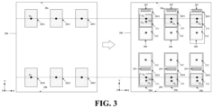
- the first pads 205 are arranged at two opposite edges of the semiconductor functional structure. Illustratively, referring to FIG. 3 , a left side of the arrow in FIG. 3 shows an example of an arrangement of the first pads 205, which is the same as FIG. 2B and is not repeated here.
- the N second pads are divided into two parts, namely a third part and a fourth part.
- the third part includes M1 second pads.
- the fourth part includes M2 second pads.
- the M1 second pads in the third part are arranged side by side along the first direction near the first edge of the semiconductor functional structure.
- the M2 second pads in the fourth part are arranged side by side along the second direction near the second edge of the semiconductor functional structure.
- the N third pads are divided into two parts, namely a fifth part and a sixth part.
- the fifth part includes M1 third pads.
- the sixth part includes M2 third pads.
- the M1 third pads in the fifth part and the M1 second pads are arranged side by side along the second direction near the first edge of the semiconductor functional structure.
- the M2 third pads in the sixth part and the M2 second pads are arranged side by side along the second direction near the second edge of the semiconductor functional structure.
- a right side of the arrow in FIG. 3 shows an example of an arrangement of the redistribution layers 206.
- the six redistribution layers 206 are divided into two parts. Each of the parts includes three redistribution layers, the three redistribution layers 206 in each part are arranged side by side along the X-axis direction, and each of the redistribution layers 206 includes a second pad 211 and a corresponding one of the third pads 212.
- the second pad 211 and the third pad 212 are arranged side by side along the Y-axis direction. Dotted lines in FIG. 3 show straight lines where the center points of the first pads 205 are located.
- all the first pads 205, the second pads 211 and the third pads 212 are of strip shapes.
- a shape of an orthographic projection of each of the redistribution layers on a plane where the interconnect layer is located is of a strip shape.
- a width of each of the first pads 205 along the first direction may be the same as a width of each of the second pads 211 and each of the third pads 212 along the first direction.
- a length of each of the first pads 205 along the second direction may be different from a length of each of the second pads 211 and each of the third pads 212 along the second direction.
- an orthographic projection of a center point of each of the second pads on the plane where the interconnect layer is located is offset by a first distance along the second direction with respect to a center point of a corresponding first pad.
- the center point O 2 of each of the second pads is offset by the first distance H1 along the Y-axis direction relative to the center point O 1 of the corresponding first pad.
- the center point O 2 of each of the second pads is offset by the first distance H1 along the Y-axis direction relative to the center point O 1 of the corresponding first pad.
- first ends of the some first pads near the first edge and second ends of the some redistribution layers near the first edge are substantially flush along a third direction perpendicular to both the first direction and the second direction.
- Third ends of the other first pads near the second edge and fourth ends of the other redistribution layers near the second edge are substantially flush along the third direction.
- second pads are located near the second ends and third pads are located away from the second ends.
- second pads are located near the fourth ends and third pads are located away from the fourth ends.
- the third pads are located near the second ends and the second pads are located away from the second ends. In the other redistribution layers, the third pads are located near the fourth ends and the second pads are located away from the fourth ends.
- the second pad may also be provided at a farther distance from the first pad.
- each of the redistribution layers further includes a first region for conductively connecting with the first pad.
- both the second pad and the third pad located on one same side of the first region.
- the second pad and the third pad are respectively located on two sides of the first region.
- the first region 213 is in contact with the conductive pillar 207 and is located around the conductive pillar, so as to realize electrical connection between each of the first pad and the redistribution layer.
- the first region 213 is located within the via hole 204.
- a material of the first region 213 may be the same as or different from the material of the redistribution layer 206 and may be any suitable conductive material.
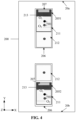
- the relative position relationships between the second pads and the third pads are different.
- the second pad in part of the package structure, is located between the conductive pillar and the third pad; in another part of the package structure, the conductive pillar 207 is located between the second pad 211 and the third pad 212.
- the first region 213 may be disposed between a corresponding second pad 211 and third pad 212, or may be disposed on a same side of the corresponding second pad 211 and third pad 212.
- the partition wall may be provided between the corresponding second pad 211 and third pad 212.
- FIG. 4 only shows one redistribution layer near the first edge 20a and one redistribution layer near the second edge 20b.
- FIG. 3 and FIG. 4 only schematically show the redistribution layer(s) near the first edge 20a and the corresponding redistribution layer(s) near the second edge 20b, the distance between them does not represent a distance in actual application. The actual distance may be set according to actual needs.
- the positions of the second pad and the third pad are different at different edges.
- a semiconductor device includes a package structure as described in the forgoing embodiments of the disclosure with a semiconductor functional structure.
- the semiconductor device further includes a base plate and a plurality of dies that are stacked.
- Each of the dies includes a semiconductor functional structure in a package structure.
- Each of the dies is electrically connected to the base plate through wires on third pads in the package structure.
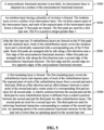
- a method for manufacturing a package structure includes the following operations.
- a semiconductor functional structure is provided.
- the top surface of the interconnect layer serves as the top surface of the semiconductor functional structure.
- an isolation layer having a plurality of via holes is formed.
- the isolation layer covers a surface of the interconnect layer.
- the via holes expose parts of the interconnect layer, and each of the parts of the interconnect layer exposed by the via holes corresponds to one first pad.
- N first pads are formed. The first pads are used for performing a first type test.
- the N is a positive integer greater than 1.
- N redistribution layers are formed on the N first pads and the isolation layer.
- Each of the redistribution layers covers the isolation layer and is electrically connected with a corresponding one of the N first pads.
- Some first pads are arranged side by side along a first direction near a first edge of the semiconductor functional structure.
- Other first pads are arranged side by side along the first direction at positions near a second edge of the semiconductor functional structure.
- the first edge and the second edge are two opposite edges of the semiconductor functional structure.
- a first insulating layer is formed.
- the first insulating layer covers the redistribution layers and exposes parts of each of the redistribution layers.
- the exposed parts of the redistribution layer form a second pad and a third pad. Both an offset direction and an offset distance between a center point of the second pad and a center point of a corresponding first pad are same for all second pads
- a relative position between the second pads and the third pads in parts of the redistribution layers is different from a relative position between the second pads and the third pads in other parts of the redistribution layers.
- the second pads are used for performing a second type test.
- the third pads are used for achieving functional interaction corresponding to a content of the second type test.
- An operating speed of the semiconductor functional structure for the first type test is lower than an operating speed of the semiconductor functional structure for the second type test.
- FIG. 5 are not exclusive and that other operations may be performed before, after, or between any of the operations shown in FIG. 5 .
- the order of the operations shown in FIG. 2 can be adjusted according to actual needs.
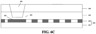
- FIG. 6A to FIG. 6D are cross-sectional schematic diagrams of a process for manufacturing a package structure provided by embodiments of the disclosure. The method for manufacturing the package structure provided by the embodiments of the disclosure will be described in detail with reference to FIG. 5 and FIG. 6A to FIG. 6D .
- a semiconductor functional structure 600 which includes a semiconductor functional layer 601 and a interconnect layer 602.
- the operation of providing a semiconductor functional structure 600 includes the following operations.
- a substrate (not shown in FIG. 6A ) is provided.
- a semiconductor functional layer 601 is formed on the substrate.
- a interconnect layer 602 is formed on the semiconductor functional layer.
- the semiconductor functional layer 601 includes a single layer thin film or multiple layer thin films.
- the semiconductor functional layer has a conductive layer and/or a dielectric layer.
- functional structures may be provided according to actual needs.
- the interconnect layer 602 is used to lead out electrical signals of the functional structures in the semiconductor functional layer 601 to operate the functional structures.
- the interconnect layer 602 includes a top metal layer, not only for leading out the electrical signals from the functional structure but also for supporting the semiconductor functional structure 600.
- the method further includes removing part of the interconnect layer 602 to reduce an area of the interconnect layer and reduce a parasitic capacitance generated by the interconnect layer.
- FIG. 6A is a cross-sectional view of a certain section after the part of the interconnect layer 602 are removed.
- the interconnect layer are not truncated, but are interconnected, that is, the interconnect layer may be continuous on other sections.
- an isolation layer 603 is formed on the interconnect layer 602.
- a material of the isolation layer includes, but is not limited to, tetraethyl orthosilicate.
- a shape of the via hole 604 may be cylindrical, inverted trapezoidal, or any suitable shape.
- a cross-sectional area of the via hole includes an area of an orthographic projection of the via hole on the plane where the interconnect layer is located. For example, when the via hole is of an inverted trapezoidal shape, the cross-sectional area of the first pad is the minimum cross-sectional area of the via hole.
- the first pads 605 are used to perform a first type test. Also, in an example not forming part of the present invention but useful for understanding it, the first pads 205 can be used to achieve functional interaction corresponding to a content of the first type test, for example, signal interaction and lead out of bonding wires.
- the first type test may be understood as some tests performed on the semiconductor functional structure at a lower operating speed. It is to be noted that, in a memory, an operating speed refers to a read-write speed of the memory.
- redistribution layers 606 are formed on the isolation layer 603 and in the via holes 604.
- a specific manner of forming the redistribution layers 606 on the isolation layer 603 includes the following operations.
- a new wire pattern is formed on the isolation layer by exposure and development, and then the redistribution layers are formed according to the new wire pattern by using an electroplating technique.
- the redistribution layers include new wire paths which are electrically connected with the interconnect layer.
- Each of the redistribution layers 606 covers the isolation layer 603 and is electrically connected to a corresponding one of the N first pads 605.
- the first pads 605 include first part of the first pads and second part of the first pads.
- the first pads in the first part of the first pads are arranged side by side along a first direction near a first edge of the semiconductor functional structure.
- the first pads in the second part of the first pads are arranged side by side along the first direction at positions near a second edge of the semiconductor functional structure.
- the first edge and the second edge are two opposite edges of the semiconductor functional structure.
- a first insulating layer 608 is formed on the redistribution layers 606.
- the exposed parts of the redistribution layer form a second pad 611 and a third pad 612.
- the second pad 611 is used for performing a second type test
- the third pad 612 is used for achieving functional interactions corresponding to a content of the second type test.
- the second type test may be understood as some tests performed on the semiconductor functional structure at a higher operating speed.
- the positions of the second pad 611 and the third pad 612 may be selected and set according to actual needs.
- the first insulating layer not only exposes parts of the redistribution layer to form the second pad and the third redistribution layer, but also exposes another part of the redistribution layer located above the first pad, so as to subsequently fill a second insulating layer 610 in a groove 609 formed by the redistribution layer.
- a density of the second insulating layer may be less than or equal to that of the first insulating layer.
- the first insulating layer also covers a bottom and a sidewall of the groove 609formed by the redistribution layer, and the second insulating layer 610 is subsequently formed in the groove 609 formed by the first insulating layer.
- the package structure also includes a conductive pillar. Accordingly, the method further includes the following operation.
- the conductive pillar is formed on the first pads after the first type test.
- the operation that the redistribution layers are formed on the first pads and the isolation layer includes that the redistribution layers are formed on the isolation layer and the conductive pillars.
- the redistribution layers are electrically connected with the interconnect layer through the conductive pillars.
- the relative position relationship between the second pad and the third pad may be set according to actual needs.
- the second pad in the package structure is located between the conductive pillar and the third pad, and/or, the conductive pillar in the package structure is located between the second pad 611 and the third pad 612.
- a relative position between the second pad 611 and the third pad 612 in parts of the redistribution layers 606 and a relative position between the second pad 611 and the third pad 612 in other parts of the redistribution layers 606 may be the same or different, which have been described before and are not repeated here.
- Both an offset direction and an offset distance between a center point of a second pad and a center point of a corresponding first pad are same for all the second pads.
- a same set of probe cards can be aligned with the center points of all the second pads 211 after moving a certain distance from the center points of the first pads 205 to a certain direction. That is, the second type test can be directly performed by the probe cards on all the second pads without replacing new probe cards.
- a package structure compatible with the two types of tests is adopted, such that a semiconductor functional structure can be subjected to different types of tests at different process stages.
- the disclosed apparatus and methods may be implemented in a non-target manner.
- the embodiments of the device described above are only schematic.
- the division of the unit is only a logical function division, and there may be another division mode in actual implementation, such as: multiple units or components can be combined, or integrated into another system, or some features can be ignored or not executed, as long as the requirements of the claims are met.
- the components shown or discussed are coupled with each other, or directly coupled.
- the units described above as separate elements may or may not be physically separated, and the elements displayed as elements may or may not be physical elements, i.e. may be located in one place or may be distributed over multiple network elements. According to the actual needs, some or all of the units can be selected to achieve the purpose of the solutions of the embodiments.
- N first pads are provided in a top metal layer, the first pads are used for a test on the semiconductor functional structure at a first operating speed. Parts of the first pads are arranged side by side along a first direction near a first edge of the semiconductor functional structure. Other parts of the first pads are arranged side by side along the first direction at positions near a second edge of the semiconductor functional structure. After the test at the first operating speed is completed, the second pads corresponding to the first pads one by one are provided in the redistribution layers on the first pads for performing a test on the semiconductor functional structure at a second operating speed.
- a relative position between the second pads and the third pads in parts of the redistribution layers is different from a relative position between the second pads and the third pads in other parts of the redistribution layers.
- Both an offset direction and an offset distance between a center point of a second pad and a center point of a corresponding first pad are same for all the second pads.
- a first pad and the corresponding second pad keeps a same relative position for all the N first pads and N second pads.
- relative positions between the second pad and the third pad located at different edges are different. By doing so, the redistribution layers located at the two edges can keep a large fault tolerance rate, and can all be close to the edge but not beyond the edge.
- the first pads and the second pads are ensured to be in favorable positions which are beneficial to saving a total area, and meanwhile, a same set of probe cards may be used for tests at the two different operating speeds. Compared with using two sets of probe cards to test separately, test cost and time are saved, and production cycle and manufacturing cost are reduced.
Landscapes
- Engineering & Computer Science (AREA)
- Manufacturing & Machinery (AREA)
- Internal Circuitry In Semiconductor Integrated Circuit Devices (AREA)
- Automation & Control Theory (AREA)
- Structures Or Materials For Encapsulating Or Coating Semiconductor Devices Or Solid State Devices (AREA)
- Testing Or Measuring Of Semiconductors Or The Like (AREA)
- Semiconductor Integrated Circuits (AREA)
Claims (13)
- Gehäusestruktur, umfassendeine funktionelle Halbleiterstruktur (200, 600),wobei diefunktionelle Halbleiterstruktur (200, 600) eine funktionelle Halbleiterstruktur (201, 601) und eine Verbindungsschicht (202, 602) umfasst, und die obereOberfläche der Verbindungsschicht (202, 602) als obere Oberfläche der funktionellen Halbleiterstruktur (200, 600) dient, wobei die Gehäusestruktur ferner
Folgendes umfasst:eine Isolierschicht (203, 603), die N Durchgangslöcher (204, 604) aufweist, wobei die Isolierschicht (203, 603) eine Oberfläche der Verbindungsschicht (202, 602) bedeckt, unddie Durchgangslöcher (204, 604)Teile der Verbindungsschicht (202, 602) freilegen;N erste Kontaktflächen (205, 605), wobei jede der ersten Kontaktflächen (205, 605) durch die Verbindungsschicht (202, 602) gebildet ist, die durch eines der Durchgangslöcher (204, 604) freigelegt ist, undN ist eine positiveeine ganze Zahl größer als 1 ist.N-Umverteilungsschichten (206, 606) auf den N ersten Kontaktflächen (205, 605),wobei jede der Umverteilungsschichten (206, 606)der N-Umverteilungsschichten (206, 606)die Isolierschicht (203, 603) bedecktund elektrisch mit einem entsprechenden der N ersten Kontaktflächen (205, 605) verbunden ist, einige erste Kontaktflächen nebeneinander entlang einer ersten Richtung in der Nähe eines ersten Randes der funktionellen Halbleiterstruktur (200, 600) angeordnet sind, andere erste Kontaktflächen nebeneinander entlang der ersten Richtung in der Nähe eines zweiten Rands der funktionellen Halbleiterstruktur (200, 600) angeordnet sind, der erste Rand und der zweite Rand zwei gegenüberliegende Ränder der funktionellen Halbleiterstruktur (200, 600) sind;
eine erste Isolierschicht (208, 608), die die Umverteilungsschichten (206, 606) bedeckt
undTeile jeder der Umverteilungsschichten (206, 606) freilegt;
undzweite Kontaktflächen (211, 611) und dritte Kontaktflächen (212, 612), wobei die freiliegenden Teile jeder der Umverteilungsschichten (206, 606)eine zweite Kontaktfläche (211, 611) und eine dritte Kontaktfläche (212,612) bilden, wobei sowohl eine Versatzrichtung als auch ein Versatzabstand zwischen einem Mittelpunkt der zweiten Kontaktfläche (211, 611) und einem Mittelpunkt einer entsprechenden ersten Kontaktfläche (205, 605)
für allezweiten Kontaktflächen (211, 611) gleich sind, eine relative Position zwischen der zweiten Kontaktfläche (211, 611) und der dritten Kontaktfläche (212, 612) für einige der Umverteilungsschichten von einer relativen Position zwischen der zweiten Kontaktfläche (211, 611) und der dritten Kontaktfläche (212, 612) für andere Umverteilungsschichten verschieden ist; die ersten Kontaktflächen (205, 605) und die zweiten Kontaktflächen (211, 611) zum Testen der funktionellen Halbleiterstruktur (200, 600) bei unterschiedlichen Betriebsgeschwindigkeiten verwendet werden, und die dritten Kontaktflächen (212, 612) zum Erreichen einer funktionellen Interaktion verwendet werden, die den von den zweiten Kontaktflächen (211, 611) getesteten Inhalten entspricht. - Gehäusestruktur nach Anspruch 1, wobei die zweiten Kontaktflächen (211, 611) und die dritten Kontaktflächen (212,
612), die in jeder der N-Umverteilungsschichten (206, 606) enthalten sind,
Seite an Seite
entlang einer zweiten Richtung angeordnet sind, wobei die zweite Richtung senkrecht zu der ersten Richtung ist. - Gehäusestruktur nach Anspruch 2, wobei eine orthografische Projektion des Mittelpunkts von
jeder der zweiten Kontaktfläche
(211, 611) auf einer Ebene, auf der sich die Verbindungsschicht (202, 602) befindet, um einen ersten Abstand entlang der zweiten Richtung in Bezug auf den Mittelpunkt der entsprechenden ersten Kontaktfläche (205, 605) versetzt ist. - Gehäusestruktur nach Anspruch 3, wobei eine orthografische Projektion jeder der Umverteilungsschichten (206, 606)
auf der Ebene, auf der sich die Verbindungsschicht (202, 602) befindet,
von der Form eines Streifens ist. - Gehäusestruktur nach Anspruch 4,wobei die ersten Enden einiger der ersten Kontaktflächen (205, 605) in der Nähe des ersten Rands und zweite Enden von
einigen der Umverteilungsschichten (206, 606)in der Nähe des ersten Rands im Wesentlichen bündig entlang einer dritten Richtung senkrecht zu der ersten und der zweiten Richtung sind; undwobei dritte Enden der anderen ersten Kontaktflächen (205, 605) in der Nähe des zweiten Rands und vierte Enden der
anderen Umverteilungsschichten (206, 606)in der Nähe des zweiten Rands entlang der dritten Richtung im Wesentlichen bündig sind. - Gehäusestruktur nach Anspruch 5,wobei sich in einigen der Umverteilungsschichten (206, 606)die zweiten Kontaktflächen (211, 611)
in der Nähe der zweiten Enden befinden und sich die dritten Kontaktflächen (212, 612) entfernt von den zweiten Enden befinden; undwobei sich in den anderen Umverteilungsschichten (206, 606),die zweiten Kontaktflächen (211, 611) in der Näheder vierten Enden befinden und sich die dritten Kontaktflächen (212, 612) entfernt von den vierten Enden befinden. - Gehäusestruktur nach Anspruch 6,wobei jede Umverteilungsschicht (206, 606)ferner einen ersten Bereich (213)
zum leitenden Verbinden mit der entsprechenden ersten Kontaktfläche (205, 605) umfasst; undwobei sich in einigen der Umverteilungsschichten (206, 606)die zweiten Kontaktflächen (211, 611) und die drittenKontaktflächen (212, 612) auf einer Seite der ersten Bereiche (213) befinden, und sich in den anderen Umverteilungsschichten (206, 606)die zweiten Kontaktflächen (211, 611) und die dritten Kontaktflächen (212, 612) jeweils an zwei Seiten der ersten Bereiche (213) befinden. - Gehäusestruktur nach Anspruch 1,wobei jede Umverteilungsschicht (206, 606)die entsprechende erste
Kontaktfläche (205, 605) direkt berührt; oderwobei die Gehäusestruktur außerdem leitende Säulen
(207) umfasst, wobei sich dieDie entsprechende leitende Säule (207) zwischen der entsprechenden Umverteilungsschicht (206, 606) und derentsprechende erste Kontaktfläche (205, 605) befindet und die Umverteilungsschicht (206, 606)elektrischüber die leitende Säule (207) mit der Verbindungsschicht (202, 602) verbunden ist. - Gehäusestruktur nach Anspruch 8, wobei die Gehäusestruktur die
Vielzahl von leitenden Säulen (207) umfasst, und die Vielzahl von leitenden Säulen (207) nebeneinander entlang der ersten Richtung angeordnet sind. - Gehäusestruktur nach Anspruch 8, wobei jede Umverteilungsschicht (206, 606)die entsprechende erste Kontaktfläche (205, 605) direkt berührt, und die Gehäusestruktur Ferner Folgendes umfasst:zweite Isolierschichten (210, 610), die sich in Rillen (209, 609) befinden, wobei jede der Rillen (209, 609) von der entsprechenden Umverteilungsschicht (206, 606) umgeben ist,eine Härteeines Materials der zweiten Isolierschichten (210, 610) geringer ist als eine Härte eines Materials der Umverteilungsschichten (206, 606).
- Halbleitervorrichtung, dadurch gekennzeichnet, dass die Halbleitervorrichtung die Gehäusestruktur nach einem der Ansprüche 1 bis 10 umfasst.
- Halbleiterstruktur nach Anspruch 11, ferner umfassend:eine Grundplatte; undeine Vielzahl von übereinander gestapelten Matrizen, wobei jede der Matrizen die Gehäusestruktur umfasst,wobei jede der Matrizen über Drähte an den dritten Kontaktflächen (212, 612) in der Gehäusestruktur elektrisch mit der Grundplatte verbunden ist.
- Verfahren zur Herstellung einer Gehäusestruktur nach Anspruch 1, die Gehäusestruktur umfassendeine funktionelle Halbleiterstruktur (200, 600),wobei die funktionelle Halbleiterstruktur (200, 600)eine funktionelle Halbleiterstruktur (201, 601) und eineVerbindungsschicht (202, 602) umfasst, und die obere Oberfläche der Verbindungsschicht (202, 602) als die obere Oberfläche der funktionellen Halbleiterstruktur (200, 600) dient, das Verfahren umfassend:Bilden einer Isolierschicht (203, 603),die N Durchgangslöcher (204, 604) aufweist, wobei die Isolierschicht (203, 603)eine Oberfläche der Verbindungsschicht (202, 602) bedeckt, die Durchgangslöcher (204, 604) Teile der Verbindungsschicht (202, 602) freilegen und jeder der freigelegten Teile der Verbindungsschicht (202, 602) eine erste Kontaktfläche (205, 605) bildet, N erste Kontaktflächen (205, 605) gebildet werden; die ersten Kontaktflächen (205, 605) für eine erste Typprüfung verwendet werden und das N eine positive ganze Zahl größer als 1 ist;Bilden von N-Umverteilungsschichten (206, 606) auf den N ersten Kontaktflächen (205, 605) und der Isolierschicht (203, 603) nach der ersten Typprüfung, wobei jede der Umverteilungsschichten (206, 606)die Isolierschicht (203, 603) bedeckt und elektrisch mit einer entsprechenden der N ersten Kontaktflächen (205, 605) verbunden ist, wobei einige der ersten Kontaktflächen (205, 605) nebeneinanderentlang einer ersten Richtung in der Nähe einer ersten Kante der funktionellen Halbleiterstruktur (200, 600) angeordnet sind, andere erste Kontaktflächen nebeneinander entlang der ersten Richtung in der Nähe einer zweiten Kante der funktionellen Halbleiterstruktur (200, 600) angeordnet sind und der erste Rand und der zweite Rand zwei gegenüberliegende Ränder der funktionellen Halbleiterstruktur (200, 600) sind; undBilden einer ersten Isolierschicht (208, 608), die die Umverteilungsschichten (206, 606) bedecktund Teile von jeder der Umverteilungsschichten (206, 606) freilegt,wobei die freiliegenden Teile jeder der Umverteilungsschichten (206, 606)eine zweite Kontaktfläche (211, 611) und eine dritte Kontaktfläche (212, 612) bilden; sowohl eine Versatzrichtung als auch ein Versatzabstand zwischen einem Mittelpunkt der zweiten Kontaktfläche (211, 611) und einem Mittelpunkt einer entsprechenden ersten Kontaktfläche (205, 605) für alle zweiten Kontaktflächen (211, 611) gleich sind; eine relative Position zwischen der zweiten Kontaktfläche (211, 611) und der dritten Kontaktflächen (212, 612) für einige der Umverteilungsschichten sich von einer relativen Position zwischen der zweiten Kontaktfläche (211, 611) und der dritten Kontaktfläche (212, 612) für andere Umverteilungsschichten unterscheidet; die zweiten Kontaktflächen (211, 611) für eine zweite Typprüfung verwendet werden, dritte Kontaktflächen (212, 612) für die Durchführung einer funktionellen Interaktion verwendet werden, die dem Inhalt der zweiten Typprüfung entspricht; und eine Betriebsgeschwindigkeit der funktionellen Halbleiterstruktur (200, 600) für die erste Typprüfung niedriger ist als eine Betriebsgeschwindigkeit für die zweite Typprüfung.
Applications Claiming Priority (2)
| Application Number | Priority Date | Filing Date | Title |
|---|---|---|---|
| CN202210619084.1A CN117199053A (zh) | 2022-06-01 | 2022-06-01 | 封装结构及其制作方法、半导体器件 |
| PCT/CN2022/102515 WO2023231122A1 (zh) | 2022-06-01 | 2022-06-29 | 封装结构及其制作方法、半导体器件 |
Publications (3)
| Publication Number | Publication Date |
|---|---|
| EP4307352A1 EP4307352A1 (de) | 2024-01-17 |
| EP4307352A4 EP4307352A4 (de) | 2024-03-20 |
| EP4307352B1 true EP4307352B1 (de) | 2025-05-07 |
Family
ID=88977077
Family Applications (1)
| Application Number | Title | Priority Date | Filing Date |
|---|---|---|---|
| EP22836031.9A Active EP4307352B1 (de) | 2022-06-01 | 2022-06-29 | Gehäusestruktur, dafür vorgesehenes herstellungsverfahren und halbleiterbauelement |
Country Status (4)
| Country | Link |
|---|---|
| US (1) | US20230395441A1 (de) |
| EP (1) | EP4307352B1 (de) |
| JP (1) | JP7576152B2 (de) |
| KR (1) | KR102774939B1 (de) |
Families Citing this family (1)
| Publication number | Priority date | Publication date | Assignee | Title |
|---|---|---|---|---|
| CN117976660B (zh) * | 2024-03-27 | 2024-06-21 | 湖北江城实验室 | 一种半导体结构及其热测试方法 |
Family Cites Families (10)
| Publication number | Priority date | Publication date | Assignee | Title |
|---|---|---|---|---|
| JPH04253353A (ja) * | 1991-01-28 | 1992-09-09 | Mitsubishi Electric Corp | 半導体集積回路装置 |
| JPH0917834A (ja) * | 1995-06-30 | 1997-01-17 | Sony Corp | 評価用素子群およびこれを用いた評価方法 |
| US6534853B2 (en) * | 2001-06-05 | 2003-03-18 | Chipmos Technologies Inc. | Semiconductor wafer designed to avoid probed marks while testing |
| JP2007115958A (ja) * | 2005-10-21 | 2007-05-10 | Seiko Epson Corp | 半導体装置 |
| JP2007115957A (ja) * | 2005-10-21 | 2007-05-10 | Seiko Epson Corp | 半導体装置及びその製造方法 |
| KR100800473B1 (ko) * | 2006-06-30 | 2008-02-04 | 삼성전자주식회사 | 재배선 칩 패드를 갖는 적층 칩 및 이를 이용한 적층 칩패키지 |
| US20090033346A1 (en) * | 2007-07-30 | 2009-02-05 | Ping-Chang Wu | Group probing over active area pads arrangement |
| KR101006521B1 (ko) * | 2008-06-30 | 2011-01-07 | 주식회사 하이닉스반도체 | 반도체 패키지 및 이의 제조 방법 |
| US9673093B2 (en) * | 2013-08-06 | 2017-06-06 | STATS ChipPAC Pte. Ltd. | Semiconductor device and method of making wafer level chip scale package |
| KR102398663B1 (ko) * | 2015-07-09 | 2022-05-16 | 삼성전자주식회사 | 칩 패드, 재배선 테스트 패드 및 재배선 접속 패드를 포함하는 반도체 칩 |
-
2022
- 2022-06-29 KR KR1020227040889A patent/KR102774939B1/ko active Active
- 2022-06-29 JP JP2023501542A patent/JP7576152B2/ja active Active
- 2022-06-29 EP EP22836031.9A patent/EP4307352B1/de active Active
-
2023
- 2023-02-02 US US18/163,802 patent/US20230395441A1/en active Pending
Also Published As
| Publication number | Publication date |
|---|---|
| EP4307352A1 (de) | 2024-01-17 |
| KR102774939B1 (ko) | 2025-02-28 |
| JP7576152B2 (ja) | 2024-10-30 |
| EP4307352A4 (de) | 2024-03-20 |
| KR20230168259A (ko) | 2023-12-13 |
| JP2024523066A (ja) | 2024-06-28 |
| US20230395441A1 (en) | 2023-12-07 |
Similar Documents
| Publication | Publication Date | Title |
|---|---|---|
| CN102881660B (zh) | 半导体器件及测试方法 | |
| KR101524318B1 (ko) | 적층된 칩 패키지들을 제조하는 방법 | |
| TWI778550B (zh) | 三維積體電路封裝及其製造方法 | |
| CN107818965B (zh) | 半导体封装件及制造再分布图案的方法 | |
| TWI857381B (zh) | 封裝結構及其製作方法、半導體器件 | |
| EP4307352B1 (de) | Gehäusestruktur, dafür vorgesehenes herstellungsverfahren und halbleiterbauelement | |
| US20230395543A1 (en) | Package structure and manufacturing method thereof, and semiconductor device | |
| EP4307351B1 (de) | Verpackungsstruktur, verpackungsverfahren und halbleiterbauelement | |
| TWI826243B (zh) | 封裝結構及其製作方法 | |
| TWI865948B (zh) | 封裝結構及其製作方法、半導體器件 | |
| US20240145399A1 (en) | Semiconductor wafer including monitoring pattern structure with cover pattern layer and contact patterns disposed over monitoring pattern structure | |
| RU2826108C2 (ru) | Пакетная структура, способ сборки пакета и полупроводниковое устройство | |
| EP4307367A1 (de) | Verpackungsstruktur und herstellungsverfahren dafür sowie halbleiterbauelement | |
| US12424538B2 (en) | Semiconductor device including dummy deep trench capacitors and a method of manufacturing thereof | |
| EP4156260B1 (de) | Passivierungsschicht mit topologischem rissstop | |
| US20230307856A1 (en) | Low profile impedance-tunable and cross-talk controlled high speed hybrid socket interconnect | |
| US20240128198A1 (en) | Semiconductor wafer including alignment key pattern layer including contact pattern layer disposed thereon | |
| US20230069294A1 (en) | Multi-die communications couplings using a single bridge die | |
| CN117198988A (zh) | 封装结构、封装方法及半导体器件 | |
| US20040217452A1 (en) | Semiconductor chip arrangement and a method for its production | |
| TW202549570A (zh) | 半導體裝置 | |
| JP2014192295A (ja) | 半導体装置 |
Legal Events
| Date | Code | Title | Description |
|---|---|---|---|
| STAA | Information on the status of an ep patent application or granted ep patent |
Free format text: STATUS: UNKNOWN |
|
| STAA | Information on the status of an ep patent application or granted ep patent |
Free format text: STATUS: THE INTERNATIONAL PUBLICATION HAS BEEN MADE |
|
| PUAI | Public reference made under article 153(3) epc to a published international application that has entered the european phase |
Free format text: ORIGINAL CODE: 0009012 |
|
| STAA | Information on the status of an ep patent application or granted ep patent |
Free format text: STATUS: REQUEST FOR EXAMINATION WAS MADE |
|
| 17P | Request for examination filed |
Effective date: 20230113 |
|
| AK | Designated contracting states |
Kind code of ref document: A1 Designated state(s): AL AT BE BG CH CY CZ DE DK EE ES FI FR GB GR HR HU IE IS IT LI LT LU LV MC MK MT NL NO PL PT RO RS SE SI SK SM TR |
|
| A4 | Supplementary search report drawn up and despatched |
Effective date: 20240221 |
|
| RIC1 | Information provided on ipc code assigned before grant |
Ipc: H01L 23/00 20060101ALI20240215BHEP Ipc: H01L 23/544 20060101ALI20240215BHEP Ipc: H01L 21/66 20060101AFI20240215BHEP |
|
| GRAP | Despatch of communication of intention to grant a patent |
Free format text: ORIGINAL CODE: EPIDOSNIGR1 |
|
| STAA | Information on the status of an ep patent application or granted ep patent |
Free format text: STATUS: GRANT OF PATENT IS INTENDED |
|
| RIC1 | Information provided on ipc code assigned before grant |
Ipc: H01L 23/00 20060101ALI20241126BHEP Ipc: H01L 21/66 20060101AFI20241126BHEP |
|
| DAV | Request for validation of the european patent (deleted) | ||
| DAX | Request for extension of the european patent (deleted) | ||
| INTG | Intention to grant announced |
Effective date: 20241206 |
|
| P01 | Opt-out of the competence of the unified patent court (upc) registered |
Free format text: CASE NUMBER: APP_1877/2025 Effective date: 20250111 |
|
| GRAS | Grant fee paid |
Free format text: ORIGINAL CODE: EPIDOSNIGR3 |
|
| GRAA | (expected) grant |
Free format text: ORIGINAL CODE: 0009210 |
|
| STAA | Information on the status of an ep patent application or granted ep patent |
Free format text: STATUS: THE PATENT HAS BEEN GRANTED |
|
| AK | Designated contracting states |
Kind code of ref document: B1 Designated state(s): AL AT BE BG CH CY CZ DE DK EE ES FI FR GB GR HR HU IE IS IT LI LT LU LV MC MK MT NL NO PL PT RO RS SE SI SK SM TR |
|
| REG | Reference to a national code |
Ref country code: GB Ref legal event code: FG4D |
|
| REG | Reference to a national code |
Ref country code: CH Ref legal event code: EP |
|
| REG | Reference to a national code |
Ref country code: DE Ref legal event code: R096 Ref document number: 602022014463 Country of ref document: DE |
|
| REG | Reference to a national code |
Ref country code: IE Ref legal event code: FG4D |
|
| PGFP | Annual fee paid to national office [announced via postgrant information from national office to epo] |
Ref country code: DE Payment date: 20250618 Year of fee payment: 4 |
|
| PGFP | Annual fee paid to national office [announced via postgrant information from national office to epo] |
Ref country code: AT Payment date: 20250721 Year of fee payment: 4 |
|
| REG | Reference to a national code |
Ref country code: NL Ref legal event code: MP Effective date: 20250507 |
|
| PG25 | Lapsed in a contracting state [announced via postgrant information from national office to epo] |
Ref country code: PT Free format text: LAPSE BECAUSE OF FAILURE TO SUBMIT A TRANSLATION OF THE DESCRIPTION OR TO PAY THE FEE WITHIN THE PRESCRIBED TIME-LIMIT Effective date: 20250908 Ref country code: ES Free format text: LAPSE BECAUSE OF FAILURE TO SUBMIT A TRANSLATION OF THE DESCRIPTION OR TO PAY THE FEE WITHIN THE PRESCRIBED TIME-LIMIT Effective date: 20250507 Ref country code: FI Free format text: LAPSE BECAUSE OF FAILURE TO SUBMIT A TRANSLATION OF THE DESCRIPTION OR TO PAY THE FEE WITHIN THE PRESCRIBED TIME-LIMIT Effective date: 20250507 |
|
| REG | Reference to a national code |
Ref country code: LT Ref legal event code: MG9D |
|
| PG25 | Lapsed in a contracting state [announced via postgrant information from national office to epo] |
Ref country code: GR Free format text: LAPSE BECAUSE OF FAILURE TO SUBMIT A TRANSLATION OF THE DESCRIPTION OR TO PAY THE FEE WITHIN THE PRESCRIBED TIME-LIMIT Effective date: 20250808 Ref country code: NO Free format text: LAPSE BECAUSE OF FAILURE TO SUBMIT A TRANSLATION OF THE DESCRIPTION OR TO PAY THE FEE WITHIN THE PRESCRIBED TIME-LIMIT Effective date: 20250807 |
|
| PG25 | Lapsed in a contracting state [announced via postgrant information from national office to epo] |
Ref country code: PL Free format text: LAPSE BECAUSE OF FAILURE TO SUBMIT A TRANSLATION OF THE DESCRIPTION OR TO PAY THE FEE WITHIN THE PRESCRIBED TIME-LIMIT Effective date: 20250507 Ref country code: NL Free format text: LAPSE BECAUSE OF FAILURE TO SUBMIT A TRANSLATION OF THE DESCRIPTION OR TO PAY THE FEE WITHIN THE PRESCRIBED TIME-LIMIT Effective date: 20250507 |
|
| REG | Reference to a national code |
Ref country code: AT Ref legal event code: MK05 Ref document number: 1793460 Country of ref document: AT Kind code of ref document: T Effective date: 20250507 |
|
| PG25 | Lapsed in a contracting state [announced via postgrant information from national office to epo] |
Ref country code: BG Free format text: LAPSE BECAUSE OF FAILURE TO SUBMIT A TRANSLATION OF THE DESCRIPTION OR TO PAY THE FEE WITHIN THE PRESCRIBED TIME-LIMIT Effective date: 20250507 |
|
| PG25 | Lapsed in a contracting state [announced via postgrant information from national office to epo] |
Ref country code: HR Free format text: LAPSE BECAUSE OF FAILURE TO SUBMIT A TRANSLATION OF THE DESCRIPTION OR TO PAY THE FEE WITHIN THE PRESCRIBED TIME-LIMIT Effective date: 20250507 Ref country code: AT Free format text: LAPSE BECAUSE OF FAILURE TO SUBMIT A TRANSLATION OF THE DESCRIPTION OR TO PAY THE FEE WITHIN THE PRESCRIBED TIME-LIMIT Effective date: 20250507 |
|
| PGFP | Annual fee paid to national office [announced via postgrant information from national office to epo] |
Ref country code: FR Payment date: 20250701 Year of fee payment: 4 |
|
| PG25 | Lapsed in a contracting state [announced via postgrant information from national office to epo] |
Ref country code: RS Free format text: LAPSE BECAUSE OF FAILURE TO SUBMIT A TRANSLATION OF THE DESCRIPTION OR TO PAY THE FEE WITHIN THE PRESCRIBED TIME-LIMIT Effective date: 20250807 |
|
| PG25 | Lapsed in a contracting state [announced via postgrant information from national office to epo] |
Ref country code: IS Free format text: LAPSE BECAUSE OF FAILURE TO SUBMIT A TRANSLATION OF THE DESCRIPTION OR TO PAY THE FEE WITHIN THE PRESCRIBED TIME-LIMIT Effective date: 20250907 |
|
| PG25 | Lapsed in a contracting state [announced via postgrant information from national office to epo] |
Ref country code: LV Free format text: LAPSE BECAUSE OF FAILURE TO SUBMIT A TRANSLATION OF THE DESCRIPTION OR TO PAY THE FEE WITHIN THE PRESCRIBED TIME-LIMIT Effective date: 20250507 |
|
| REG | Reference to a national code |
Ref country code: DE Ref legal event code: R079 Ref document number: 602022014463 Country of ref document: DE Free format text: PREVIOUS MAIN CLASS: H01L0021660000 Ipc: H10P0074000000 |
|
| PG25 | Lapsed in a contracting state [announced via postgrant information from national office to epo] |
Ref country code: SM Free format text: LAPSE BECAUSE OF FAILURE TO SUBMIT A TRANSLATION OF THE DESCRIPTION OR TO PAY THE FEE WITHIN THE PRESCRIBED TIME-LIMIT Effective date: 20250507 Ref country code: DK Free format text: LAPSE BECAUSE OF FAILURE TO SUBMIT A TRANSLATION OF THE DESCRIPTION OR TO PAY THE FEE WITHIN THE PRESCRIBED TIME-LIMIT Effective date: 20250507 |
|
| PG25 | Lapsed in a contracting state [announced via postgrant information from national office to epo] |
Ref country code: CZ Free format text: LAPSE BECAUSE OF FAILURE TO SUBMIT A TRANSLATION OF THE DESCRIPTION OR TO PAY THE FEE WITHIN THE PRESCRIBED TIME-LIMIT Effective date: 20250507 |
|
| PG25 | Lapsed in a contracting state [announced via postgrant information from national office to epo] |
Ref country code: EE Free format text: LAPSE BECAUSE OF FAILURE TO SUBMIT A TRANSLATION OF THE DESCRIPTION OR TO PAY THE FEE WITHIN THE PRESCRIBED TIME-LIMIT Effective date: 20250507 |
|
| PG25 | Lapsed in a contracting state [announced via postgrant information from national office to epo] |
Ref country code: SK Free format text: LAPSE BECAUSE OF FAILURE TO SUBMIT A TRANSLATION OF THE DESCRIPTION OR TO PAY THE FEE WITHIN THE PRESCRIBED TIME-LIMIT Effective date: 20250507 |
|
| REG | Reference to a national code |
Ref country code: CH Ref legal event code: H13 Free format text: ST27 STATUS EVENT CODE: U-0-0-H10-H13 (AS PROVIDED BY THE NATIONAL OFFICE) Effective date: 20260127 |
|
| PG25 | Lapsed in a contracting state [announced via postgrant information from national office to epo] |
Ref country code: IT Free format text: LAPSE BECAUSE OF FAILURE TO SUBMIT A TRANSLATION OF THE DESCRIPTION OR TO PAY THE FEE WITHIN THE PRESCRIBED TIME-LIMIT Effective date: 20250507 |
|
| REG | Reference to a national code |
Ref country code: DE Ref legal event code: R097 Ref document number: 602022014463 Country of ref document: DE |
|
| PG25 | Lapsed in a contracting state [announced via postgrant information from national office to epo] |
Ref country code: LU Free format text: LAPSE BECAUSE OF NON-PAYMENT OF DUE FEES Effective date: 20250629 |
|
| PG25 | Lapsed in a contracting state [announced via postgrant information from national office to epo] |
Ref country code: MC Free format text: LAPSE BECAUSE OF FAILURE TO SUBMIT A TRANSLATION OF THE DESCRIPTION OR TO PAY THE FEE WITHIN THE PRESCRIBED TIME-LIMIT Effective date: 20250507 |
|
| REG | Reference to a national code |
Ref country code: BE Ref legal event code: MM Effective date: 20250630 |
|
| PG25 | Lapsed in a contracting state [announced via postgrant information from national office to epo] |
Ref country code: RO Free format text: LAPSE BECAUSE OF FAILURE TO SUBMIT A TRANSLATION OF THE DESCRIPTION OR TO PAY THE FEE WITHIN THE PRESCRIBED TIME-LIMIT Effective date: 20250507 |
|
| PLBE | No opposition filed within time limit |
Free format text: ORIGINAL CODE: 0009261 |
|
| STAA | Information on the status of an ep patent application or granted ep patent |
Free format text: STATUS: NO OPPOSITION FILED WITHIN TIME LIMIT |
|
| REG | Reference to a national code |
Ref country code: CH Ref legal event code: L10 Free format text: ST27 STATUS EVENT CODE: U-0-0-L10-L00 (AS PROVIDED BY THE NATIONAL OFFICE) Effective date: 20260318 |
|
| PG25 | Lapsed in a contracting state [announced via postgrant information from national office to epo] |
Ref country code: IE Free format text: LAPSE BECAUSE OF NON-PAYMENT OF DUE FEES Effective date: 20250629 |
|
| 26N | No opposition filed |
Effective date: 20260210 |
|
| PG25 | Lapsed in a contracting state [announced via postgrant information from national office to epo] |
Ref country code: BE Free format text: LAPSE BECAUSE OF NON-PAYMENT OF DUE FEES Effective date: 20250630 |
|
| PG25 | Lapsed in a contracting state [announced via postgrant information from national office to epo] |
Ref country code: CH Free format text: LAPSE BECAUSE OF NON-PAYMENT OF DUE FEES Effective date: 20250630 |