EP4310982A1 - Batteriesystem, antriebssystem und energiespeicherbehälter - Google Patents
Batteriesystem, antriebssystem und energiespeicherbehälter Download PDFInfo
- Publication number
- EP4310982A1 EP4310982A1 EP22778654.8A EP22778654A EP4310982A1 EP 4310982 A1 EP4310982 A1 EP 4310982A1 EP 22778654 A EP22778654 A EP 22778654A EP 4310982 A1 EP4310982 A1 EP 4310982A1
- Authority
- EP
- European Patent Office
- Prior art keywords
- switch
- controllable switching
- drive
- switching transistors
- turned
- Prior art date
- Legal status (The legal status is an assumption and is not a legal conclusion. Google has not performed a legal analysis and makes no representation as to the accuracy of the status listed.)
- Granted
Links
Images





Classifications
-
- H—ELECTRICITY
- H01—ELECTRIC ELEMENTS
- H01M—PROCESSES OR MEANS, e.g. BATTERIES, FOR THE DIRECT CONVERSION OF CHEMICAL ENERGY INTO ELECTRICAL ENERGY
- H01M10/00—Secondary cells; Manufacture thereof
- H01M10/42—Methods or arrangements for servicing or maintenance of secondary cells or secondary half-cells
- H01M10/425—Structural combination with electronic components, e.g. electronic circuits integrated to the outside of the casing
- H01M10/4257—Smart batteries, e.g. electronic circuits inside the housing of the cells or batteries
-
- H—ELECTRICITY
- H01—ELECTRIC ELEMENTS
- H01M—PROCESSES OR MEANS, e.g. BATTERIES, FOR THE DIRECT CONVERSION OF CHEMICAL ENERGY INTO ELECTRICAL ENERGY
- H01M10/00—Secondary cells; Manufacture thereof
- H01M10/42—Methods or arrangements for servicing or maintenance of secondary cells or secondary half-cells
- H01M10/425—Structural combination with electronic components, e.g. electronic circuits integrated to the outside of the casing
-
- H—ELECTRICITY
- H01—ELECTRIC ELEMENTS
- H01M—PROCESSES OR MEANS, e.g. BATTERIES, FOR THE DIRECT CONVERSION OF CHEMICAL ENERGY INTO ELECTRICAL ENERGY
- H01M10/00—Secondary cells; Manufacture thereof
- H01M10/42—Methods or arrangements for servicing or maintenance of secondary cells or secondary half-cells
- H01M10/48—Accumulators combined with arrangements for measuring, testing or indicating the condition of cells, e.g. the level or density of the electrolyte
- H01M10/482—Accumulators combined with arrangements for measuring, testing or indicating the condition of cells, e.g. the level or density of the electrolyte for several batteries or cells simultaneously or sequentially
-
- H—ELECTRICITY
- H01—ELECTRIC ELEMENTS
- H01M—PROCESSES OR MEANS, e.g. BATTERIES, FOR THE DIRECT CONVERSION OF CHEMICAL ENERGY INTO ELECTRICAL ENERGY
- H01M50/00—Constructional details or processes of manufacture of the non-active parts of electrochemical cells other than fuel cells, e.g. hybrid cells
- H01M50/20—Mountings; Secondary casings or frames; Racks, modules or packs; Suspension devices; Shock absorbers; Transport or carrying devices; Holders
- H01M50/204—Racks, modules or packs for multiple batteries or multiple cells
-
- H—ELECTRICITY
- H01—ELECTRIC ELEMENTS
- H01M—PROCESSES OR MEANS, e.g. BATTERIES, FOR THE DIRECT CONVERSION OF CHEMICAL ENERGY INTO ELECTRICAL ENERGY
- H01M50/00—Constructional details or processes of manufacture of the non-active parts of electrochemical cells other than fuel cells, e.g. hybrid cells
- H01M50/50—Current conducting connections for cells or batteries
- H01M50/572—Means for preventing undesired use or discharge
- H01M50/574—Devices or arrangements for the interruption of current
- H01M50/583—Devices or arrangements for the interruption of current in response to current, e.g. fuses
-
- H—ELECTRICITY
- H02—GENERATION; CONVERSION OR DISTRIBUTION OF ELECTRIC POWER
- H02J—ELECTRIC POWER NETWORKS; CIRCUIT ARRANGEMENTS OR SYSTEMS FOR SUPPLYING OR DISTRIBUTING ELECTRIC POWER; SYSTEMS FOR STORING ELECTRIC ENERGY
- H02J7/00—Circuit arrangements for charging or discharging batteries or for supplying loads from batteries
- H02J7/50—Circuit arrangements for charging or discharging batteries or for supplying loads from batteries acting upon multiple batteries simultaneously or sequentially
-
- H—ELECTRICITY
- H02—GENERATION; CONVERSION OR DISTRIBUTION OF ELECTRIC POWER
- H02J—ELECTRIC POWER NETWORKS; CIRCUIT ARRANGEMENTS OR SYSTEMS FOR SUPPLYING OR DISTRIBUTING ELECTRIC POWER; SYSTEMS FOR STORING ELECTRIC ENERGY
- H02J7/00—Circuit arrangements for charging or discharging batteries or for supplying loads from batteries
- H02J7/50—Circuit arrangements for charging or discharging batteries or for supplying loads from batteries acting upon multiple batteries simultaneously or sequentially
- H02J7/52—Circuit arrangements for charging or discharging batteries or for supplying loads from batteries acting upon multiple batteries simultaneously or sequentially for charge balancing, e.g. equalisation of charge between batteries
- H02J7/54—Passive balancing, e.g. using resistors or parallel MOSFETs
-
- H—ELECTRICITY
- H02—GENERATION; CONVERSION OR DISTRIBUTION OF ELECTRIC POWER
- H02J—ELECTRIC POWER NETWORKS; CIRCUIT ARRANGEMENTS OR SYSTEMS FOR SUPPLYING OR DISTRIBUTING ELECTRIC POWER; SYSTEMS FOR STORING ELECTRIC ENERGY
- H02J7/00—Circuit arrangements for charging or discharging batteries or for supplying loads from batteries
- H02J7/60—Circuit arrangements for charging or discharging batteries or for supplying loads from batteries including safety or protection arrangements
- H02J7/62—Circuit arrangements for charging or discharging batteries or for supplying loads from batteries including safety or protection arrangements against overcurrent
-
- H—ELECTRICITY
- H02—GENERATION; CONVERSION OR DISTRIBUTION OF ELECTRIC POWER
- H02J—ELECTRIC POWER NETWORKS; CIRCUIT ARRANGEMENTS OR SYSTEMS FOR SUPPLYING OR DISTRIBUTING ELECTRIC POWER; SYSTEMS FOR STORING ELECTRIC ENERGY
- H02J7/00—Circuit arrangements for charging or discharging batteries or for supplying loads from batteries
- H02J7/60—Circuit arrangements for charging or discharging batteries or for supplying loads from batteries including safety or protection arrangements
- H02J7/663—Circuit arrangements for charging or discharging batteries or for supplying loads from batteries including safety or protection arrangements using battery or load disconnect circuits
-
- H—ELECTRICITY
- H01—ELECTRIC ELEMENTS
- H01M—PROCESSES OR MEANS, e.g. BATTERIES, FOR THE DIRECT CONVERSION OF CHEMICAL ENERGY INTO ELECTRICAL ENERGY
- H01M10/00—Secondary cells; Manufacture thereof
- H01M10/42—Methods or arrangements for servicing or maintenance of secondary cells or secondary half-cells
- H01M10/425—Structural combination with electronic components, e.g. electronic circuits integrated to the outside of the casing
- H01M2010/4271—Battery management systems including electronic circuits, e.g. control of current or voltage to keep battery in healthy state, cell balancing
-
- H—ELECTRICITY
- H01—ELECTRIC ELEMENTS
- H01M—PROCESSES OR MEANS, e.g. BATTERIES, FOR THE DIRECT CONVERSION OF CHEMICAL ENERGY INTO ELECTRICAL ENERGY
- H01M10/00—Secondary cells; Manufacture thereof
- H01M10/42—Methods or arrangements for servicing or maintenance of secondary cells or secondary half-cells
- H01M10/425—Structural combination with electronic components, e.g. electronic circuits integrated to the outside of the casing
- H01M2010/4278—Systems for data transfer from batteries, e.g. transfer of battery parameters to a controller, data transferred between battery controller and main controller
-
- H—ELECTRICITY
- H01—ELECTRIC ELEMENTS
- H01M—PROCESSES OR MEANS, e.g. BATTERIES, FOR THE DIRECT CONVERSION OF CHEMICAL ENERGY INTO ELECTRICAL ENERGY
- H01M2200/00—Safety devices for primary or secondary batteries
- H01M2200/10—Temperature sensitive devices
- H01M2200/103—Fuse
-
- H—ELECTRICITY
- H02—GENERATION; CONVERSION OR DISTRIBUTION OF ELECTRIC POWER
- H02J—ELECTRIC POWER NETWORKS; CIRCUIT ARRANGEMENTS OR SYSTEMS FOR SUPPLYING OR DISTRIBUTING ELECTRIC POWER; SYSTEMS FOR STORING ELECTRIC ENERGY
- H02J3/00—Circuit arrangements for AC mains or AC distribution networks
- H02J3/28—Arrangements for balancing of the load in networks by storage of energy
- H02J3/32—Arrangements for balancing of the load in networks by storage of energy using batteries or super capacitors with converting means
-
- Y—GENERAL TAGGING OF NEW TECHNOLOGICAL DEVELOPMENTS; GENERAL TAGGING OF CROSS-SECTIONAL TECHNOLOGIES SPANNING OVER SEVERAL SECTIONS OF THE IPC; TECHNICAL SUBJECTS COVERED BY FORMER USPC CROSS-REFERENCE ART COLLECTIONS [XRACs] AND DIGESTS
- Y02—TECHNOLOGIES OR APPLICATIONS FOR MITIGATION OR ADAPTATION AGAINST CLIMATE CHANGE
- Y02E—REDUCTION OF GREENHOUSE GAS [GHG] EMISSIONS, RELATED TO ENERGY GENERATION, TRANSMISSION OR DISTRIBUTION
- Y02E60/00—Enabling technologies; Technologies with a potential or indirect contribution to GHG emissions mitigation
- Y02E60/10—Energy storage using batteries
Definitions
- This application relates to the field of power electronics technologies, and in particular, to a battery system, a drive system, and an energy storage container.
- the battery pack is used in a plurality of fields such as energy storage power stations, home energy storage, or electric vehicles.
- a battery system usually includes a plurality of battery packs, and the plurality of battery packs may be connected in series to obtain a high voltage.
- Each battery pack usually includes a first switch that is connected in series to the battery pack and a second switch that is connected in parallel to the battery pack.
- the first switch is configured to rectify a fault.
- the second switch is configured to bypass the corresponding battery pack.
- the first switch and the second switch each may be a metal-oxide-semiconductor field-effect transistor (MOS, Metal-Oxide-Semiconductor Field-Effect Transistor).
- MOS Metal-Oxide-Semiconductor Field-Effect Transistor
- the first switch and the second switch each may be implemented through a plurality of MOS transistors that are connected in parallel.
- pass-through may occur in the first switch and the second switch when a fault occurs, in other words, both the first switch and the second switch are turned on. This is equivalent to that two ends of the battery pack are directly short-circuited.
- a continuous short circuit or a long-time short circuit causes a permanent failure of the battery pack.
- the first switch and the second switch may cause an electric arc risk because of a short circuit failure.
- this application provides a battery system, a drive system, and a control method. This can avoid or eliminate a direct short circuit between a positive electrode and a negative electrode of a battery pack, and ensure safety of the battery pack.
- An embodiment of this application provides a battery system, including a plurality of battery packs that are connected in series. Each battery pack corresponds to one first switch and one second switch. Each battery pack is connected in series to the corresponding first switch and then connected in parallel to the second switch. A single switching transistor may bear a limited current. Therefore, in an actual product, each of the first switch and the second switch includes a plurality of controllable switching transistors that are connected in parallel, so that each of the first switch and the second switch may bear a large current.
- the plurality of controllable switching transistors in the first switch and the second switch provided in this embodiment of this application are not simultaneously turned on, but are turned on in batches.
- the plurality of controllable switching transistors included in the first switch correspond to at least two different turn-on moments
- the plurality of controllable switching transistors included in the second switch correspond to at least two different turn-on moments. Due to a manufacturing process problem of a switching transistor with a low on-resistance (Rdson) and a large-capacity packaging problem, the plurality of controllable switching transistors each may be independently packaged.
- the plurality of controllable switching transistors in the second switch are turned on in batches. Because the first switch is turned on, a current of the entire battery system is large, and a controllable switching transistor that is first turned on in the second switch is turned off because of an excessively large current flowing through the controllable switching transistor, that is, the controllable switching transistor is automatically turned off. In this way, the second switch is not turned on, and a state in which the first switch and the second switch are simultaneously turned on does not exist. Therefore, the battery pack is not short-circuited for a long time. This ensures safety of the battery pack.
- switching states of the controllable switching transistors in the first switch and the second switch are separately controlled by corresponding drive signals.
- the plurality of controllable switching transistors are turned on in batches. For example, the plurality of controllable switching transistors are turned on when the drive signals are at a high level, and are turned off when the drive signals are at a low level, that is, rising edges of the drive signals may be set asynchronous, to not simultaneously turn on the plurality of controllable switching transistors. That is, the plurality of controllable switching transistors included in the first switch correspond to at least two drive signals that have different rising edges.
- the plurality of controllable switching transistors included in the second switch correspond to at least two drive signals that have different rising edges.
- the plurality of controllable switching transistors may be simultaneously turned off at a turn-off moment.
- turn-off moments of the plurality of controllable switching transistors included in the first switch are the same, and turn-off moments of the plurality of controllable switching transistors included in the second switch are the same.
- the turn-off moment corresponds to a falling edge of the drive signal.
- Falling edges of the drive signals may be set synchronous, to simultaneously turn off the plurality of controllable switching transistors when the drive signals are at a low level. For example, both the first switch and the second switch are turned off when the corresponding drive signals are at a low level. Falling edges of the drive signals of the plurality of controllable switching transistors included in the first switch all are the same. Falling edges of the drive signals of the plurality of controllable switching transistors included in the second switch all are the same.
- a quantity of drive signals is the same as a quantity of controllable switching transistors, the drive signals are in a one-to-one correspondence with the controllable switching transistors, and the quantity of drive signals is less than or equal to a quantity of drive circuits.
- a quantity of drive circuits corresponding to the first switch is the same as a quantity of controllable switching transistors included in the first switch, the drive circuits corresponding to the first switch are in a one-to-one correspondence with the controllable switching transistors included in the first switch, and the quantity of drive circuits corresponding to the first switch is greater than or equal to a quantity of drive signals corresponding to the first switch.
- a quantity of drive circuits corresponding to the second switch is the same as a quantity of controllable switching transistors included in the second switch, the drive circuits corresponding to the second switch are in a one-to-one correspondence with the controllable switching transistors included in the second switch, and the quantity of drive circuits corresponding to the second switch is greater than or equal to a quantity of drive signals corresponding to the second switch.
- the quantity of drive circuits is less than the quantity of controllable switching transistors, the quantity of drive circuits is the same as the quantity of drive signals, and the drive circuits are in a one-to-one correspondence with the drive signals.
- the plurality of controllable switching transistors included in the first switch correspond to at least two drive circuits, and the at least two drive circuits corresponding to the first switch are in a one-to-one correspondence with the at least two drive signals corresponding to the first switch.
- the plurality of controllable switching transistors included in the second switch correspond to at least two drive circuits, and the at least two drive circuits corresponding to the second switch are in a one-to-one correspondence with the at least two drive signals corresponding to the second switch.
- both the first switch and the second switch include M controllable switching transistors that are connected in parallel.
- M is an integer greater than or equal to 2.
- a maximum quantity of controllable switching transistors driven by each drive circuit is M/2.
- the battery system may further include: a controller.
- the controller is configured to: control the first switch to be turned off; control a first batch of controllable switching transistors in the plurality of controllable switching transistors in the second switch to be turned on; and when it is detected that the first batch of controllable switching transistors to be turned on are successfully turned on, control other controllable switching transistors in the second switch to be successively turned on in batches.
- the first switch may not be successfully turned off. Therefore, the first batch of controllable switching transistors in the second switch may not be successfully turned on.
- the first switch may be successfully turned off, but the first batch of controllable switching transistors in the second switch cannot be successfully turned on because of a fault.
- the controller may identify, through a voltage at two ends of the first switch, whether the first switch is successfully turned off.
- the voltage at the two ends of the first switch is large, that is, the voltage at the two ends of the first switch is greater than a preset voltage threshold. This indicates that the first switch is successfully turned off.
- the plurality of controllable switching transistors in the second switch are controlled to be turned on in batches.
- the battery system further includes a current detection circuit.
- the current detection circuit is used to detect a current that flows through E controllable switching transistors in the first switch when the first switch is turned on. E is an integer less than or equal to M/2.
- the first switch includes M controllable switching transistors that are connected in parallel. M is an integer greater than or equal to 2.
- the controller is further configured to: when the current that flows through the E controllable switching transistors in the first switch is greater than a preset current threshold, control the first switch to be turned off.
- a value of E may be usually an integer less than or equal to a half of M. For example, to reduce costs, the value of E may be 1 for ease of detection.
- the first switch includes the plurality of controllable switching transistors that are connected in parallel.
- a total current of the first switch is a sum of currents of the plurality controllable switching transistors that are connected in parallel, and a trunk current of the first switch is greater than a current of a branch in which each controllable switching transistor is located.
- the current of the branch in which the controllable switching transistor is located is small.
- the current detection circuit is easy to implement. A requirement on hardware is low. In addition, a size of a corresponding current detection circuit for detection of a small current is small. This saves a volume of the entire battery system, and saves space. Therefore, the current detection circuit provided in this embodiment of this application is easy to implement and has low costs.
- the battery system further includes a fuse.
- the second switch is connected in series to the fuse, or each controllable switching transistor in the second switch is connected in series to the fuse.
- the fuse melts when a current is excessively large, to protect an MOS transistor and the battery pack.
- the first switch may also be connected in series to the fuse, or each controllable switching transistor in the first switch is connected in series to the fuse.
- a quantity of fuses is not limited in this embodiment of this application. Generally, to reduce costs and facilitate manufacturing, only the second switch is connected in series to the fuse, that is, one fuse is connected in series to a trunk of the second switch.
- an embodiment of this application further provides a drive system for a battery pack.
- Advantages and effects of the foregoing battery system are also applicable to the following drive system. Details are not described herein again.
- the drive system is used to drive a switch in the battery pack.
- the battery pack corresponds to a first switch and a second switch.
- the battery pack is connected in series to the first switch and then connected in parallel to the second switch.
- the drive system includes a controller and a drive circuit.
- the first switch includes a plurality of controllable switching transistor that are connected in parallel.
- the second switch includes a plurality of controllable switching transistors that are connected in parallel.
- the controller is configured to control the drive circuit to drive the plurality of controllable switching transistors included in the first switch to correspond to at least two different turn-on moments, and is further configured to control the drive circuit to drive the plurality of controllable switching transistors included in the second switch to correspond to at least two different turn-on moments.
- the drive circuit includes at least two first drive circuits and at least two second drive circuits.
- the at least two first drive circuits are used to respectively drive different controllable switching transistors in the first switch based on at least two drive signals of a first group of drive signals that are generated by the controller and that have different rising edges.
- the at least two second drive circuits are used to respectively drive different controllable switching transistors in the second switch based on at least two drive signals of a second group of drive signals that are generated by the controller and that have different rising edges.
- falling edges of the at least two drive signals of the first group of drive signals that have different rising edges are the same. Falling edges of the at least two drive signals of the second group of drive signals that have different rising edges are the same.
- a quantity of drive circuits corresponding to the first switch is the same as a quantity of controllable switching transistors included in the first switch, the drive circuits corresponding to the first switch are in a one-to-one correspondence with the controllable switching transistors included in the first switch, and the quantity of drive circuits corresponding to the first switch is greater than or equal to a quantity of drive signals corresponding to the first switch.
- a quantity of drive circuits corresponding to the second switch is the same as a quantity of controllable switching transistors included in the second switch, the drive circuits corresponding to the second switch are in a one-to-one correspondence with the controllable switching transistors included in the second switch, and the quantity of drive circuits corresponding to the second switch is greater than or equal to a quantity of drive signals corresponding to the second switch.
- the plurality of controllable switching transistors included in the first switch correspond to at least two drive circuits, and the at least two drive circuits corresponding to the first switch are in a one-to-one correspondence with the at least two drive signals corresponding to the first switch.
- the plurality of controllable switching transistors included in the second switch correspond to at least two drive circuits, and the at least two drive circuits corresponding to the second switch are in a one-to-one correspondence with the at least two drive signals corresponding to the second switch.
- a maximum quantity of controllable switching transistors driven by each drive circuit is M/2.
- An embodiment of this application further provides an energy storage container, including the battery system described above.
- each batch of controllable switching transistors that are turned on correspond to a different turn-on moment.
- the first switch is already turned on, a current of the entire battery system is large, and a batch of controllable switching transistors that are first turned on in the second switch automatically are turned off because of an excessively large current flowing through the batch of controllable switching transistors.
- the second switch is not successfully turned on, a state in which the first switch and the second switch are simultaneously turned on does not exist, and a positive electrode and a negative electrode of the battery pack are not short-circuited together. Therefore, the battery pack is not short-circuited for a long time. This ensures safety of the battery pack.
- first”, “second”, and the like are used only for descriptive purposes, and cannot be understood as an indication or implication of relative importance or an implicit indication of a quantity of indicated technical features. Therefore, a feature limited by “first”, “second”, or the like may explicitly or implicitly include one or more features. In descriptions of this application, unless otherwise stated, "a plurality of" means two or more than two.
- connection needs to be understood in a broad sense unless otherwise expressly specified and limited.
- connection may be a fixed connection, or may be a detachable connection or an integrated connection; and may be a direct connection, or may be an indirect connection through an intermediate medium.
- a term “coupling” may be a manner of implementing an electrical connection for signal transmission. The “coupling” may be a direct electrical connection, or may be an indirect electrical connection through an intermediate medium.
- An embodiment of this application relates to a battery system, and in particular, to a manner of controlling serially-connected switches of a battery pack and parallel-connected switches of the battery pack in the battery system.
- An application scenario of the battery system is not limited in this embodiment of this application.
- the application scenario may be an energy storage power station, photovoltaic energy storage, home energy storage, or a power battery pack in an electric vehicle.
- FIG. 1 is a schematic diagram of a battery system according to an embodiment of this application.
- the battery system provided in this embodiment of this application includes N battery packs that are connected in series.
- N is an integer greater than or equal to 2.
- the N battery packs are a first battery pack 101, a second battery pack 102 to an N th battery pack 10N.
- a positive electrode of the first battery pack 101 is connected to a battery bus, a negative electrode of the first battery pack 101 is connected to a positive electrode of the second battery pack 102, and so on, until an (N-1) th battery pack (not shown in the figure) is connected to a positive electrode of the N th battery pack 10N, and a negative electrode of the N th battery pack 10N is grounded.
- the first battery pack further includes a first switch S1 that is connected in series to the first battery BAT1. That is, a negative electrode of the first battery BAT1 is connected to a first end of the first switch S1, and a second end of the first switch S1 is connected to a positive electrode of a second battery BAT2 in the second battery pack 102.
- the first battery BAT1 is connected in series to the first switch S1 and then connected in parallel to a second switch S2. That is, a first end of the second switch S2 is connected to a positive electrode of the first battery BAT1, and a second end of the second switch S2 is connected to the second end of the first switch S1.
- the first switch S1 in each battery pack is turned on. That is, all batteries are connected in series to form a voltage of the battery bus.
- the first switch S1 that is connected in series to the first battery BAT1 is turned off, to cut off a fault.
- the second switch S2 that is connected in parallel to the first battery BAT1 needs to be controlled to be turned on. That is, the second switch S2 is configured to bypass the faulty first battery BAT1.
- the second switch S2 that is turned on may provide a current path for the normal battery pack, so that the normal battery pack is connected to the battery bus.
- the first battery pack 101 may be connected to a positive battery bus through a fuse FU and a circuit breaker Q that are connected in series.
- the fuse R may melt when a circuit is excessively large, to implement overcurrent protection.
- the circuit breaker Q may be turned off during maintenance protection, to avoid a risk of an electric shock.
- each of the first switch S1 and the second switch S2 is usually implemented by using an MOS transistor.
- a single MOS transistor may bear a limited current. Therefore, one single switch, for example, the first switch S1 usually needs to be implemented by connecting a plurality of MOS transistors in parallel.
- the second switch S2 also includes a plurality of MOS transistors that are connected in parallel.
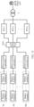
- FIG. 2 is a schematic diagram of an internal structure of a battery pack according to an embodiment of this application.
- each battery pack in FIG. 1 may include a battery BAT, a first switch S1, and a second switch S2.
- the first switch S1 and the second switch S2 are both MOS transistors, and both include an anti-parallel diode.
- FIG. 3 is a schematic diagram of a battery pack according to an embodiment of this application.
- both a first switch and a second switch When a battery system is applied to a low-voltage and high-power scenario, especially a large-current scenario, both a first switch and a second switch usually include a plurality of controllable switching transistors that are connected in parallel, to improve a current handling capability.
- a plurality of controllable switching transistors are usually separately packaged. That is, the first switch and the second switch are separately implemented by connecting a plurality of small packaged controllable switching transistors in parallel.
- both the first switch S1 and the second switch S2 include M MOS transistors that are connected in parallel is used for description.
- the first switch S1 in FIG. 2 includes an MOS transistor S1_1, an MOS transistor S1_2, an MOS transistor S1_3 to an MOS transistor S1_M in FIG. 3 .
- the second switch S2 in FIG. 2 includes an MOS transistor S2_1, an MOS transistor S2_2, an MOS transistor S2_3 to an MOS transistor S2_M in FIG. 3 .
- M is not specifically limited in this embodiment of this application.
- M may be an integer greater than or equal to 2. Whether a quantity of MOS transistors included in the first switch and a quantity of MOS transistors included in the second switch are the same is not limited in this embodiment of this application. In this embodiment of this application, only an example in which both the first switch and the second switch include M MOS transistors is used for description.
- each battery pack further includes a drive circuit and a control circuit of the first switch and the second switch.
- a first drive circuit 201 is used to drive all MOS transistors in the first switch.
- a second drive circuit 202 is used to drive all MOS transistors in the second switch.
- a controller 100 is configured to generate an S1 drive signal of the first switch and an S2 drive signal of the second switch. That is, the controller 100 sends the S1 drive signal to the first drive circuit 201, and sends the S2 drive signal to the second drive circuit 202.
- the first drive circuit 201 drives all the MOS transistors in the first switch based on the S1 drive signal.
- the second drive circuit 202 drives all the MOS transistors in the second switch based on the S2 drive signal. That is, switching states, namely, on states and off states, of all the MOS transistors in the first switch and the second switch are controlled.
- All the MOS transistors in the first switch correspond to a same S1 drive signal. Therefore, all the MOS transistors in the first switch operate simultaneously.
- all the MOS transistors in the second switch correspond to a same S2 drive signal. Therefore, all the MOS transistors in the second switch operate simultaneously.
- the M MOS transistors included in the first switch correspond to a same drive signal, that is, the M MOS transistors are simultaneously turned off, or the M MOS transistors are simultaneously turned on. For example, when the drive signal is at a high level, the MOS transistors are turned on; or when the drive signal is at a low level, the MOS transistors are turned off.
- the first switch is turned on or the second switch is turned on, and the first switch and the second switch are not simultaneously turned on.
- the first switch and the second switch may be simultaneously turned on.
- the first switch is normally turned on, and the second switch is also turned on.
- the first switch and the second switch that are turned on directly short-circuit a positive electrode and a negative electrode of the battery pack. The battery pack is damaged because of a long-time short circuit.
- the plurality of battery packs that are connected in series form a high voltage.
- the high voltage is applied to two ends of an MOS transistor at a moment of turning off the MOS transistor, resulting in high-voltage arcing or adhesion. It is more difficult to turn off the MOS transistor.
- the first switch is turned on, a current of the entire battery system is large, and a controllable switching transistor that is first turned on in the second switch is turned off because of an excessively large current flowing through the controllable switching transistor, that is, the controllable switching transistor is automatically turned off.
- the second switch is not turned on, and the first switch and the second switch are not simultaneously turned on. Therefore, the battery pack is not short-circuited for a long time. This ensures safety of the battery pack.
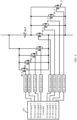
- FIG. 4 is a schematic diagram of another battery system according to an embodiment of this application.
- the battery system provided in this embodiment of this application includes a plurality of battery packs that are connected in series. Each battery pack corresponds to one first switch that is connected in series to the battery pack. Each battery pack corresponds to one second switch that is connected in parallel to the battery pack.
- Each battery pack is connected in series to the corresponding first switch and then connected in parallel to the second switch.
- the first switch includes a plurality of controllable switching transistors that are connected in parallel.
- the second switch includes a plurality of controllable switching transistors that are connected in parallel.
- a quantity of controllable switching transistors included in the first switch is not limited, and a quantity of controllable switching transistors included in the second switch is not limited.
- the quantity of controllable switching transistors included in the first switch and the quantity of controllable switching transistors included in the second switch may be the same or different.
- an example in which the quantity of controllable switching transistors included in the first switch and the quantity of controllable switching transistors included in the second switch are the same is used for description.
- a type of the controllable switching transistors is also not limited.
- the controllable switching transistors included in the first switch and the second switch may be specifically implemented by using an MOS transistor.
- the plurality of controllable switching transistors included in the first switch correspond to at least two different turn-on moments.
- the plurality of controllable switching transistors included in the second switch correspond to at least two different turn-on moments.
- Switching states of the first switch and the second switch are complementary in a normal case. That is, when the first switch is turned on, the second switch is not controlled to be turned on. When the second switch is turned on, the first switch is not controlled to be turned on. If the first switch needs to be controlled to be turned on, the second switch needs to be first controlled to be turned off. However, in an abnormal case, when the first switch is normally turned on, the second switch may also be turned on because of an abnormality. This short-circuits the battery pack. To protect the battery pack, in this embodiment of this application, the turn-on moments of the MOS transistors in the first switch and the second switch are set to be different.
- the plurality of controllable switching transistors correspond to different turn-on moments. This may be specifically implemented through different time sequences of drive signals corresponding to the controllable switching transistors. For example, for a controllable switching transistor that is turned on at a high level, moments of rising edges of the drive signals may be different. That is, the plurality of controllable switching transistors included in the first switch correspond to at least two drive signals that have different rising edges. The plurality of controllable switching transistors included in the second switch correspond to at least two drive signals that have different rising edges.
- a quantity of drive signals is the same as a quantity of MOS transistors, the drive signals are in a one-to-one correspondence with the MOS transistors, and the quantity of drive signals is less than or equal to a quantity of drive circuits. That is, a quantity of drive circuits corresponding to the first switch is the same as a quantity of controllable switching transistors included in the first switch, the drive circuits corresponding to the first switch are in a one-to-one correspondence with the controllable switching transistors included in the first switch, and the quantity of drive circuits corresponding to the first switch is greater than or equal to a quantity of drive signals corresponding to the first switch.
- a quantity of drive circuits corresponding to the second switch is the same as a quantity of controllable switching transistors included in the second switch, the drive circuits corresponding to the second switch are in a one-to-one correspondence with the controllable switching transistors included in the second switch, and the quantity of drive circuits corresponding to the second switch is greater than or equal to a quantity of drive signals corresponding to the second switch.
- a quantity of drive circuits is less than a quantity of MOS transistors, the quantity of drive circuits is the same as a quantity of drive signals, and the drive circuits are in a one-to-one correspondence with the drive signals. That is, the plurality of controllable switching transistors included in the first switch correspond to at least two drive circuits, and the at least two drive circuits corresponding to the first switch are in a one-to-one correspondence with the at least two drive signals corresponding to the first switch.
- the plurality of controllable switching transistors included in the second switch correspond to at least two drive circuits, and the at least two drive circuits corresponding to the second switch are in a one-to-one correspondence with the at least two drive signals corresponding to the second switch.
- a quantity of drive circuits is less than a quantity of MOS transistors, and the quantity of drive circuits is less than a quantity of drive signals.
- a maximum quantity of controllable switching transistors driven by each drive circuit is M/2.
- the first switch includes four MOS transistors, the four MOS transistors correspond to at least two drive circuits, and each drive circuit drives two MOS transistors.
- FIG. 1 describes in detail an implementation in which a plurality of battery packs are connected in series.
- the following uses one of the battery packs as an example to describe, with reference to FIG. 4 , a specific implementation of a battery pack provided in an embodiment of this application.
- both the first switch and the second switch include four controllable switching transistors.
- the four MOS transistors that are connected in parallel in the first switch are respectively an MOS transistor S1_1, an MOS transistor S1_2, an MOS transistor S1_3, and an MOS transistor S1_4.
- the four MOS transistors that are connected in parallel in the second switch are respectively an MOS transistor S2_1, an MOS transistor S2_2, an MOS transistor S2_3, and an MOS transistor S2_4.
- MOS transistors each include an anti-parallel diode.
- the battery pack is charged in addition to being used as a power supply to discharge.
- the anti-parallel diode of the MOS transistor is turned on. In this case, detection of a voltage at two ends of the first switch cannot completely identify whether the first switch is reliably turned off. Especially in a large-current scenario, whether the first switch is turned off cannot be accurately detected.
- the battery pack is charged, even if all MOS transistors of the first switch fail, accurate detection cannot be performed. Because both conduction of the anti-parallel diode and short-circuit impedance of the first switch affect a conduction voltage drop of the first switch, the conduction voltage drop of the first switch is unstable.
- the four MOS transistors need to correspond to at least two different drive signals.
- the four MOS transistors may correspond to two different drive signals, or three different drive signals, or four different drive signals.
- the drive signal of the MOS transistor is at a high level, the MOS transistor is turned on.
- difference of the drive signals indicates difference of rising edges of the drive signals. Therefore, the turn-on moments of the MOS transistors are different.
- each MOS transistor corresponds to one drive signal and each MOS transistor corresponds to one drive circuit is used. That is, the MOS transistor, the drive circuit, and the drive signal are in a one-to-one correspondence.
- the controller 100 is configured to output eight drive signals to eight drive circuits.
- the eight drive circuits are respectively used to drive switching states of the eight MOS transistors.
- the MOS transistor S1_1 of the first switch corresponds to an S1 drive circuit 1, and the S1 drive circuit corresponds to an S1 drive signal 1.
- the MOS transistor S1_2 corresponds to an S1 drive circuit 2, and the S1 drive circuit 2 corresponds to an S1 drive signal 2.
- the MOS transistor S1_3 corresponds to an S1 drive circuit 3, and the S1 drive circuit 3 corresponds to an S1 drive signal 3.
- the MOS transistor S1_4 corresponds to an S1 drive circuit 4, and the S1 drive circuit 4 corresponds to an S1 drive signal 4.
- the MOS transistor S2_1 of the second switch corresponds to an S2 drive circuit 1, and the S2 drive circuit corresponds to an S2 drive signal 1.
- the MOS transistor S2_2 corresponds to an S2 drive circuit 2
- the S2 drive circuit 2 corresponds to an S2 drive signal 2.
- the MOS transistor S2_3 corresponds to an S2 drive circuit 3
- the S2 drive circuit 3 corresponds to an S2 drive signal 3.
- the MOS transistor S2_4 corresponds to an S2 drive circuit 4, and the S2 drive circuit 4 corresponds to an S2 drive signal 4.
- the four MOS transistors of the first switch are all turned on, and the four MOS transistors of the second switch are all turned off.
- S2_1 may be turned on. Because the four MOS transistors of the first switch are all turned on, a current passing through S2_1 is large. A single MOS transistor may bear a limited current. Therefore, S2_1 is turned off. In this way, the positive electrode and the negative electrode of the battery pack are not short-circuited together. This ensures safety of the battery pack.
- the drive signals corresponding to the MOS transistors are different, that is, corresponding turn-on moments are different. Therefore, a probability that the drive signals or drive circuits of all the MOS transistors of the second switch are abnormal is small, and a probability that the battery pack is short-circuited may be reduced to some extent.
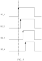
- FIG. 5 is a time sequence diagram of drive signals of MOS transistors in a second switch according to an embodiment of this application.
- drive signals of four MOS transistors included in the second switch have different rising edges, and successively lag preset time.
- a drive signal of an MOS transistor S2_2 lags behind a drive signal of an MOS transistor S2_1.
- a drive signal of an MOS transistor S2_3 lags behind the drive signal of the MOS transistor S2_2.
- a drive signal of an MOS transistor S2_4 lags behind the drive signal of the MOS transistor S2_3. That is, in a normal case, the MOS transistor S2_1, the MOS transistor S2_2, the MOS transistor S2_3, and the MOS transistor S2_4 are successively controlled to be turned on.
- FIG. 5 shows only a time sequence of the drive signals of the MOS transistors in the second switch.
- a time sequence of drive signals of MOS transistors in a first switch may also be similar.
- FIG. 5 is only an example of the time sequence of the four MOS transistors, and lag time of the drive signals of the four MOS transistors may be consistent or inconsistent.
- a specific turn-on sequence of the four MOS transistors is not limited, provided that the four MOS transistors are not turned on at a same moment.
- FIG. 5 uses an example in which S2_1 is turned on first, and S2_2 is turned on later. For example, S2_2 may be turned on first, and S2_1 is turned on later.
- a plurality of drive signals may be used to drive a battery pack, to ensure that the MOS transistors in the first switch are turned on at different moments, and the MOS transistors in the second switch are turned on at different moments.
- each MOS transistor corresponds to one drive signal, a quantity of abnormal drive signals is small, and a quantity of MOS transistors that are simultaneously turned on is small. Therefore, the battery pack may be better protected from a short circuit.
- an embodiment of this application further provides a manner of driving another battery system.
- the following provides a detailed description with reference to FIG. 6 .
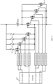
- FIG. 6 is a schematic diagram of still another battery system according to an embodiment of this application.
- a drive circuit of one battery pack includes a controller 100 and a plurality of drive circuits.
- the following still uses an example in which both a first switch and a second switch include four MOS transistors. For specific descriptions, refer to descriptions corresponding to FIG. 4 . Details are not described herein again.
- FIG. 6 It can be seen from comparison between FIG. 4 and FIG. 6 that, in FIG. 6 , two MOS transistors share a same drive circuit, and each drive circuit separately corresponds to one drive signal. That is, a quantity of drive circuits is less than a quantity of MOS transistors, and the quantity of drive circuits is the same as a quantity of drive signals.
- a first drive circuit 201 is used to drive an MOS transistor S1_1 and an MOS transistor S1_2 in the first switch based on an S1 drive signal 1.
- a second drive circuit 202 is used to drive an MOS transistor S1_3 and an MOS transistor S1_4 in the first switch based on an S1 drive signal 2.
- a third drive circuit 203 is used to drive an MOS transistor S2_1 and an MOS transistor S2_2 in the second switch based on an S2 drive signal 1.
- a fourth drive circuit 204 is used to drive an MOS transistor S2_3 and an MOS transistor S2_4 in the second switch based on an S2 drive signal 2.
- the four MOS transistors of the first switch are all turned on, and the four MOS transistors corresponding to the second switch need to be all turned off.
- drive signals or drive circuits corresponding to the second switch are abnormal, for example, the S2 drive signal 1 is abnormal, S2_1 and S2_2 are simultaneously turned on. Because the four MOS transistors of the first switch are all turned on, when S2_1 and S2_2 are turned on, S2_1 and S2_2 are turned off and not successfully turned on because of an excessively large current. In this way, a positive electrode and a negative electrode of the battery pack are not short-circuited. This ensures safety of the battery pack.
- the drive signal may be usually implemented by using a pulse width modulation (PWM, Pulse Width Modulation) signal.
- PWM pulse width modulation
- Pulse Width Modulation Pulse Width Modulation
- the controller 100 may be implemented by using a dedicated chip, such as a single-chip microcomputer or a microprocessor.
- whether turn-off moments of the MOS transistors in each switch are the same is not limited.
- the MOS transistors may be turned off, or may not be simultaneously turned off.
- a plurality of controllable switching transistors included in the first switch correspond to a same turn-off moment. That is, the plurality of controllable switching transistors are simultaneously turned off.
- a plurality of controllable switching transistors included in the second switch correspond to a same turn-off moment. That is, the plurality of controllable switching transistors are simultaneously turned off.
- the MOS transistors may be simultaneously turned off by setting falling edge moments of the drive signals corresponding to the MOS transistors to be the same. That is, the plurality of controllable switching transistors included in the first switch correspond to at least two drive signals whose falling edges are the same.
- the plurality of controllable switching transistors included in the second switch correspond to at least two drive signals whose falling edges are the same.
- turn-off moments of the four MOS transistors included in the second switch are the same. That is, falling edge moments of the drive signals corresponding to the four MOS transistors are the same.
- the drive signals are in a one-to-one correspondence with the drive circuits, and the quantity of drive circuits is less than the quantity of MOS transistors.
- the following describes a specific implementation with reference to FIG. 7 .
- FIG. 7 is a schematic diagram of yet another battery system according to an embodiment of this application.
- FIG. 7 an example in which a first switch includes four MOS transistors and a second switch includes four MOS transistors is still used.
- a description of a specific connection relationship refer to FIG. 4 . Details are not described herein again. Only differences are described in this embodiment.
- a controller 100 outputs four drive signals: an S1 drive signal 1, an S1 drive signal 2, an S2 drive signal 1, and an S2 drive signal 2. Each drive signal is simultaneously sent to two drive circuits. Each drive circuit drives one MOS transistor.
- the four MOS transistors of the first switch respectively correspond to an S1 drive circuit 1, an S1 drive circuit 2, an S1 drive circuit 3, and an S1 drive circuit 4. Both the S1 drive circuit 1 and the S1 drive circuit 2 are connected to the S1 drive signal 1. Both the S1 drive circuit 3 and the S1 drive circuit 4 are connected to the S1 drive signal 2.
- the four MOS transistors of the second switch respectively correspond to an S2 drive circuit 1, an S2 drive circuit 2, an S2 drive circuit 3, and an S2 drive circuit 4. Both the S2 drive circuit 1 and the S2 drive circuit 2 are connected to the S2 drive signal 1. Both the S2 drive circuit 3 and the S2 drive circuit 4 are connected to the S2 drive signal 2.
- S2_1 and S2_3 respectively correspond to the S2 drive signal 1 and the S2 drive signal 2. Therefore, S2_1 and S2_3 are successively turned on provided that rising edges of the S2 drive signal 1 and the S2 drive signal 2 are different.
- both S2_1 and S2_2 are abnormally turned on. Because all the MOS transistors in the first switch are turned on, when S2_1 and S2_2 are turned on, both S2_1 and S2_2 are turned off because of an excessively large current flowing through S2_1 and S2_2, that is, S2_1 and S2_2 are turned off. In this way, a positive electrode and a negative electrode of a battery pack BAT are not connected together, and the battery pack BAT is not short-circuited. This ensures safety of the battery pack BAT.
- the four MOS transistors in the first switch need to be all turned off.
- the drive signals of the first switch are abnormal, when S1_1 and S 1_2 in the first switch are turned on, the S1_3 and S1_4 in the first switch are not turned off. In this case, all currents flowing through the first switch are applied to S1_1 and S 1_2 that are turned on. Because a large current exceeds a bearing capability of S 1_1 and S1_2, S1_1 and S 1_2 are turned off. In this way, the positive electrode and the negative electrode of the battery pack BAT are not short-circuited together. This ensures safety of the battery pack BAT.
- the battery system provided in this embodiment of this application may further include a controller.
- the controller further ensures correct operations of the first switch and the second switch based on control logic.
- the controller in the battery system provided in this embodiment is configured to send a corresponding first drive signal to the first switch, and is further configured to send a corresponding second drive signal to the second switch. That is, the drive signals corresponding to the MOS transistors in the first switch and the second switch are all generated by the controller. That is, the control circuit in the foregoing figure may be implemented by the controller.
- a specific implementation of the controller is not limited in this application.
- the controller may be a single-chip microcomputer or a microprocessor, and may directly output a PWM signal as a drive signal.
- the controller is configured to: when a voltage at two ends of the first switch is abnormal, stop sending the corresponding drive signal to the first switch; and when a voltage at two ends of the second switch is abnormal, stop sending the corresponding drive signal to the second switch.
- a specific detection manner may be: When the voltage at the two ends of the first switch is less than a preset voltage threshold, it indicates that the first switch is not reliably turned on, and is still in an off state. Only when the voltage at the two ends of the first switch is greater than the preset voltage threshold, it indicates that the first switch is reliably turned off. In this case, the second switch is allowed to be controlled to be turned on.
- the second switch when the voltage at the two ends of the second switch is less than the preset voltage threshold, it indicates that the second switch is not reliably turned on, and is still in an off state. Only when the voltage at the two ends of the second switch is greater than the preset voltage threshold, it indicates that the second switch is reliably turned off. In this case, the first switch is allowed to be turned on, and the drive signal that is used to turn on the first switch is sent to the first switch.
- the controller is further configured to: when the voltage at the two ends of the first switch is greater than the preset voltage threshold, it indicates that the first switch is reliably turned off.
- a plurality of controllable switching transistors in the second switch may be controlled to be turned on in batches.
- the plurality of controllable switching transistors in the second switch are controlled to be turned on in batches, whether the plurality of controllable switching transistors in the second switch are reliably turned on may be verified. For example, after a first batch of controllable switching transistors in the second switch are controlled to be turned on, the voltage at the two ends of the second switch may be detected. When the voltage is less than a preset value, it indicates that the first batch of controllable switching transistors in the second switch are turned on, and a second batch of controllable switching transistors in the second switch are controlled to be turned on, and so on.
- the first batch of controllable switching transistors in the second switch are turned off and cannot be successfully turned on because of a large voltage. In this case, other batches of controllable switching transistors in the second switch do not need to be successively turned on, and troubleshooting may be performed on the first switch.
- the battery system provided in this embodiment of this application further includes a voltage detection circuit that is used to detect the voltage at the two ends of the first switch and the voltage at the two ends of the second switch.
- a current detection circuit may be further included.
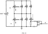
- FIG. 8 is a schematic diagram of still yet another battery system according to an embodiment of this application.
- the battery system provided in this embodiment of this application may further include a current detection circuit.
- the current detection circuit obtains a current flowing through E controllable switching transistors in a first switch when the first switch is turned on.
- E is an integer and is less than or equal to M/2.
- the first switch includes M controllable switching transistors that are connected in parallel.
- M is an integer greater than or equal to 2.
- a value of E may be usually an integer less than or equal to a half of M. For example, to reduce costs, the value of E may be 1 for ease of detection.
- the value of E may further be a common divisor of M.
- the first switch includes a plurality of MOS transistors that are connected in parallel, the current detection circuit may be used to detect a current flowing through one of the plurality of MOS transistors, to represent a value of a current of the first switch. That is, when the first switch is turned on, if a current flowing through the first switch is overcurrent, a current flowing through each MOS transistor in the first switch is overcurrent.
- the first switch includes the plurality of MOS transistors that are connected in parallel.
- a total current of the first switch is a sum of currents of the plurality of MOS transistors that are connected in parallel, and a trunk current of the first switch is greater than a current of a branch in which each MOS transistor is located.
- the current of the branch in which the MOS transistor is located is small.
- the current detection circuit is easy to implement. A requirement on hardware is low.
- a size of a corresponding current detection circuit for detection of a small current is small. This saves a volume of the entire battery system, and saves space. Therefore, the current detection circuit provided in this embodiment of this application is easy to implement and has low costs.
- the current detection circuit includes a detection resistor.
- the detection resistor is connected in series to one MOS transistor.
- the current detection circuit further includes an operational amplifier circuit.
- the operational amplifier circuit amplifies a current sampled by the current detection circuit and then outputs an amplified current, that is, a detection current Is in a specific proportion relationship with a current on the MOS transistor is obtained.
- the detection current Is may represent a value of a current flowing through the MOS transistor, and a current flowing through one MOS transistor may represent the value of the current of the first switch. In this way, whether the first switch successfully operates is determined based on the detection current.
- a controller is further configured to: when the current flowing through the first switch is greater than a preset current threshold, control the first switch to be turned off, that is, protect the first switch and a battery pack that is connected in series to the first switch, and control all MOS transistors in the first switch to be turned off.
- FIG. 8 is an equivalent schematic diagram of a single battery pack in a battery system.
- both a first switch S 1 and a second switch S2 corresponding to a battery pack BAT include a plurality of MOS transistors, it is equivalent to that the battery pack BAT is a power supply, and one MOS transistor in the first switch S1 and one MOS transistor in the second switch S2 form a half-bridge circuit.
- two MOS transistors on the half-bridge circuit are both turned on, a positive electrode and a negative electrode of the battery pack BAT are directly short-circuited.
- FIG. 9 is a schematic diagram of a further battery system according to an embodiment of this application.
- the battery system provided in this embodiment may further include a fuse.
- Each controllable switching transistor in a second switch may be connected in series to the fuse.
- S1_1 is connected in series to a first fuse FU4, S1_2 is connected in series to a second fuse FU2, S1_3 is connected in series to a second fuse FU3, and S1_4 is connected in series to a second fuse FU4.
- the fuse melts when a current is excessively large, to protect an MOS transistor and the battery pack.
- FIG. 9 is described only by using an example in which each controllable switching transistor in the second switch is connected in series to one fuse.
- the second switch may include only one fuse, and after being connected in parallel, all controllable switching transistors in the second switch are connected in series to one fuse. In this way, a quantity of fuses may be reduced, and a circuit structure is simple, to facilitate production and manufacturing.
- FIG. 9 is described by using an example in which the second switch is connected in series to a fuse.
- a first switch may also be connected in series to a fuse. Specifically, the first switch may be connected in series to only one fuse, or each controllable switching transistor in the first switch may be connected in series to one fuse.
- a quantity of fuses is not specifically limited in this embodiment of this application, and may be set by a person skilled in the art based on a requirement.
- an embodiment of this application further provides a drive system for a battery pack.
- the drive system is used to drive a switch in the battery pack.
- a plurality of battery packs are usually connected in series.
- the drive system for the battery pack provided in this embodiment of this application is applied to driving the switch in the battery pack.
- the battery pack corresponds to the first switch and the second switch.
- the battery pack is connected in series to the first switch and then connected in parallel to the second switch.
- the plurality of battery packs are connected in series by using the first switch. In a normal case, all first switches are turned on, and all second switches are turned off.
- the drive system includes a controller and a drive circuit.
- the first switch includes a plurality of controllable switching transistors that are connected in parallel.
- the second switch includes a plurality of controllable switching transistors that are connected in parallel.
- the controller is configured to control the drive circuit to drive the plurality of controllable switching transistors included in the first switch to correspond to at least two different turn-on moments, and is further configured to control the drive circuit to drive the plurality of controllable switching transistors included in the second switch to correspond to at least two different turn-on moments.
- the controller may generate a drive signal, and the drive circuit controls an operation of each controllable switching transistor based on the drive signal.
- the drive signal is a PWM signal
- the controllable switching transistor is an MOS transistor.
- the PWM signal is at a high level
- the MOS transistor is turned on.
- the PWM signal is at a low level
- the MOS transistor is turned off.
- a quantity of drive signals generated by the controller may be the same as a quantity of drive circuits, and the drive signals may be in a one-to-one correspondence with the drive circuits.
- the quantity of drive signals may be less than the quantity of drive circuits, that is, a plurality of drive circuits share a same drive signal.
- the quantity of drive circuits may be the same as a quantity of controllable switching transistors, and the drive circuits may be in a one-to-one correspondence with the controllable switching transistors, that is, one drive circuit drives one MOS transistor.
- the quantity of drive circuits may be less than the quantity of controllable switching transistors, that is, one drive circuit may simultaneously drive a plurality of MOS transistors.
- controllable switching transistors in the first switch correspond to at least two drive signals that have different rising edges, it can be ensured that the controllable switching transistors in the first switch are successively turned on in at least two batches.
- controllable switching transistors in the second switch correspond to at least two drive signals that have different rising edges, it can be ensured that the controllable switching transistors in the second switch are successively turned on in at least two batches.
- the drive circuit includes at least two first drive circuits and at least two second drive circuits.
- the at least two first drive circuits are used to respectively drive different controllable switching transistors in the first switch based on at least two drive signals of a first group of drive signals that are generated by the controller and that have different rising edges.
- the at least two second drive circuits are used to respectively drive different controllable switching transistors in the second switch based on at least two drive signals of a second group of drive signals that are generated by the controller and that have different rising edges.
- falling edges of the at least two drive signals of the first group of drive signals that have different rising edges are the same. Falling edges of the at least two drive signals of the second group of drive signals that have different rising edges are the same.
- a quantity of drive circuits corresponding to the first switch is the same as a quantity of controllable switching transistors included in the first switch, the drive circuits corresponding to the first switch are in a one-to-one correspondence with the controllable switching transistors included in the first switch, and the quantity of drive circuits corresponding to the first switch is greater than or equal to a quantity of drive signals corresponding to the first switch.
- a quantity of drive circuits corresponding to the second switch is the same as a quantity of controllable switching transistors included in the second switch, the drive circuits corresponding to the second switch are in a one-to-one correspondence with the controllable switching transistors included in the second switch, and the quantity of drive circuits corresponding to the second switch is greater than or equal to a quantity of drive signals corresponding to the second switch.
- the plurality of controllable switching transistors included in the first switch correspond to at least two drive circuits, and the at least two drive circuits corresponding to the first switch are in a one-to-one correspondence with the at least two drive signals corresponding to the first switch.
- the plurality of controllable switching transistors included in the second switch correspond to at least two drive circuits, and the at least two drive circuits corresponding to the second switch are in a one-to-one correspondence with the at least two drive signals corresponding to the second switch.
- a quantity of controllable switching transistors driven by the drive circuit is not limited in this embodiment of this application.
- the quantity of controllable switching transistors driven by the drive circuit may be one, two, three, or four.
- a maximum quantity of controllable switching transistors driven by each drive circuit is usually M/2.
- M is a total quantity of MOS transistors included in the first switch and a total quantity of MOS transistors included in the second switch.
- the following uses an example in which the battery system provided in this embodiment of this application is applied to the energy storage field for description.
- a plurality of battery packs are connected in series to form a battery cluster, and a plurality of battery clusters are disposed in an energy storage container.
- the battery cluster may be charged by using a direct current of a photovoltaic string.
- Electric energy output by the energy storage container may be fed back to an alternating current power grid through a converter, or may be provided for home use through a converter.
- the electric energy output by the energy storage container provides power for a household appliance.
- FIG. 10 is a schematic diagram of an energy storage container according to an embodiment of this application.
- An embodiment of this application further provides an energy storage container, including a plurality of battery systems.
- an energy storage container including a plurality of battery systems.
- the energy storage container includes a plurality of battery clusters.
- Each battery cluster includes a plurality of battery packs.
- a manner of controlling a first switch and a second switch corresponding to the battery pack may be the specific manner in the foregoing embodiment.
- a quantity of battery clusters included in the energy storage container is not specifically limited, and a quantity of battery packs included in each battery cluster is not limited.
- FIG. 10 is described by using an example in which six battery clusters are disposed in one energy storage container 1000.
- the six battery clusters are a battery cluster B 1 to a battery cluster B6.
- the battery clusters shown in FIG. 10 are disposed in two rows along a length direction of the energy storage container 1000.
- a first row of battery clusters includes the battery cluster B 1 to a battery cluster B3 from left to right.
- a second row of battery clusters includes a battery cluster B4 to the battery cluster B6 from right to left.
- the first row of battery clusters corresponds to a first side wall in the length direction of the energy storage container 1000.
- the second row of battery clusters corresponds to a second side wall in the length direction of the energy storage container 1000.
- Each battery cluster may include a plurality of battery packs that are connected in series.
- a quantity of battery packs included in each battery cluster is not limited in this embodiment of this application.
- the following describes an application manner of an energy storage container in which a battery cluster is disposed in the energy storage field.
- FIG. 11 is a schematic diagram of application of an energy storage container according to an embodiment of this application.
- the energy storage container 1000 provided in this embodiment includes n battery clusters, for example, a first battery cluster B1 to an n th battery cluster Bn.
- a first battery cluster B1 to an n th battery cluster Bn.
- each battery cluster includes m battery modules is used.
- the first battery cluster B1 includes a battery module ESM 1 to a battery module ESM m.
- the battery module ESM 1 to the battery module ESM m are connected in series.
- Each battery cluster is connected to an input end of a power conversion system (PCS, Power Conversion System).
- PCS Power Conversion System
- An output end of the PCS is connected to a power grid.
- the battery cluster outputs a direct current. Therefore, if the power grid is an alternating current power grid, the PCS needs to convert the direct current into an alternating current for the power grid.
- FIG. 12 is a schematic diagram of a connection between another energy storage container and a power grid according to an embodiment of this application.
- each battery cluster is connected to a corresponding direct current converter.
- a first battery cluster B1 is connected to a direct current converter 1
- a second battery cluster B1 is connected to a direct current converter 2
- an m th battery cluster Bm is connected to a direct current converter m.
- Each battery cluster includes j battery modules that are a battery module 1 to a battery module j.
- Power of each direct current converter may be different.
- the power of the direct current converter may be different from power of a power conversion system. Therefore, a junction cabinet 2000 is needed for conversion.
- a busbar is disposed in the junction cabinet 2000. Power of a single battery cluster is limited. Therefore, output ends of a plurality of power conversion systems are usually connected in parallel and then connected to an input end of a transformer T.
- the PCS completes power conversion. For example, power converted by a PCS 1 to a PCS n may be the same.
- the output ends of the plurality of PCSs are connected in parallel and then connected to the input end of the transformer T. This may increase power.
- the transformer T is configured to transform an input voltage and then feed back a transformed voltage to the power grid.
- At least one (item) refers to one or more and "a plurality of” refers to two or more.
- the term “and/or” is used for describing an association relationship between associated objects, and represents that three relationships may exist. For example, “A and/or B” may represent the following three cases: Only A exists, only B exists, and both Aand B exist, where A and B may be singular or plural.
- the character “/” generally indicates an "or” relationship between the associated objects.
- At least one of the following items (pieces) or a similar expression thereof refers to any combination of these items, including any combination of singular items (pieces) or plural items (pieces).
- At least one of a, b, or c may indicate a, b, c, a and b, a and c, b and c, or a, b, and c, where a, b, and c may be singular or plural.
Landscapes
- Engineering & Computer Science (AREA)
- Chemical & Material Sciences (AREA)
- Chemical Kinetics & Catalysis (AREA)
- Electrochemistry (AREA)
- General Chemical & Material Sciences (AREA)
- Manufacturing & Machinery (AREA)
- Power Engineering (AREA)
- Microelectronics & Electronic Packaging (AREA)
- Charge And Discharge Circuits For Batteries Or The Like (AREA)
- Battery Mounting, Suspending (AREA)
Applications Claiming Priority (2)
| Application Number | Priority Date | Filing Date | Title |
|---|---|---|---|
| CN202110333905.0A CN113258146B (zh) | 2021-03-29 | 2021-03-29 | 一种电池系统、驱动系统及储能集装箱 |
| PCT/CN2022/082186 WO2022206471A1 (zh) | 2021-03-29 | 2022-03-22 | 一种电池系统、驱动系统及储能集装箱 |
Publications (3)
| Publication Number | Publication Date |
|---|---|
| EP4310982A1 true EP4310982A1 (de) | 2024-01-24 |
| EP4310982A4 EP4310982A4 (de) | 2024-09-04 |
| EP4310982B1 EP4310982B1 (de) | 2025-09-10 |
Family
ID=77181237
Family Applications (1)
| Application Number | Title | Priority Date | Filing Date |
|---|---|---|---|
| EP22778654.8A Active EP4310982B1 (de) | 2021-03-29 | 2022-03-22 | Batteriesystem, antriebssystem und energiespeicherbehälter |
Country Status (4)
| Country | Link |
|---|---|
| US (1) | US20240021890A1 (de) |
| EP (1) | EP4310982B1 (de) |
| CN (1) | CN113258146B (de) |
| WO (1) | WO2022206471A1 (de) |
Families Citing this family (4)
| Publication number | Priority date | Publication date | Assignee | Title |
|---|---|---|---|---|
| CN113258146B (zh) * | 2021-03-29 | 2022-12-30 | 华为数字能源技术有限公司 | 一种电池系统、驱动系统及储能集装箱 |
| CN113991792B (zh) * | 2021-11-05 | 2024-08-13 | 阳光电源股份有限公司 | 一种电池单元、电池储能系统及其故障保护方法 |
| CN114069789B (zh) * | 2021-11-20 | 2023-09-22 | 傲普(上海)新能源有限公司 | 一种电池簇并联环流变压器控制电路 |
| CN117713262B (zh) * | 2023-06-06 | 2025-10-28 | 荣耀终端股份有限公司 | 一种电源管理电路及方法、电子设备和存储介质 |
Family Cites Families (30)
| Publication number | Priority date | Publication date | Assignee | Title |
|---|---|---|---|---|
| DE3584401D1 (de) * | 1984-07-24 | 1991-11-21 | Voigt & Haeffner Gmbh | Transformatorschaltung. |
| JP3286673B2 (ja) * | 1997-01-24 | 2002-05-27 | 浩 坂本 | 充電器用のコンバータ回路 |
| JP4186896B2 (ja) * | 2004-09-09 | 2008-11-26 | 株式会社デンソー | フライングキャパシタ式電池電圧検出装置 |
| US8471529B2 (en) * | 2010-10-14 | 2013-06-25 | GM Global Technology Operations LLC | Battery fault tolerant architecture for cell failure modes parallel bypass circuit |
| EP2700958B1 (de) * | 2011-04-21 | 2019-01-16 | Renesas Electronics Corporation | Schaltkreis, auswahlschaltung und spannungsmessvorrichtung |
| JP5099569B1 (ja) * | 2011-05-13 | 2012-12-19 | 独立行政法人 宇宙航空研究開発機構 | 直並列切り替え式セル電圧バランス回路のスイッチをmosfetで構成した回路及びその駆動回路 |
| DE102011089655B4 (de) * | 2011-12-22 | 2025-12-31 | Robert Bosch Gmbh | Batteriesystem und Verfahren |
| JP5971626B2 (ja) * | 2012-03-15 | 2016-08-17 | 株式会社日立製作所 | 電池システム |
| CN203014427U (zh) * | 2012-12-10 | 2013-06-19 | 王奉瑾 | 一种可串并联切换的电池组连接控制装置 |
| CN103311592B (zh) * | 2013-06-27 | 2015-08-05 | 长城汽车股份有限公司 | 动力电池系统及具有其的车辆 |
| US9564806B2 (en) * | 2013-09-25 | 2017-02-07 | Cree, Inc. | Boost converter with reduced switching loss and methods of operating the same |
| CN203617744U (zh) * | 2013-11-22 | 2014-05-28 | 江苏大学 | 用于esasre悬架分级变压充电控制的开关组 |
| US10116291B2 (en) * | 2015-08-10 | 2018-10-30 | Texas Instruments Incorporated | Reverse current protection circuit |
| CN107204638A (zh) * | 2016-03-17 | 2017-09-26 | 德龙伟创科技(深圳)有限公司 | 一种电池保护电路 |
| CN205811601U (zh) * | 2016-06-28 | 2016-12-14 | 维沃移动通信有限公司 | 充电控制电路、充电装置和移动终端 |
| KR101837469B1 (ko) * | 2016-11-04 | 2018-03-12 | (주)성진아이엘 | 순차 별 스위칭 제어를 통해 과부하의 방지가 가능한 정류기 |
| CN106374588B (zh) * | 2016-11-17 | 2018-04-10 | 深圳市盈动力科技有限公司 | 一种高压锂电池包故障的安全管理系统 |
| CN107425562A (zh) * | 2017-06-07 | 2017-12-01 | 安徽锐能科技有限公司 | 用于电池阵列下电的系统 |
| CN107294164A (zh) * | 2017-07-07 | 2017-10-24 | 东莞中汽宏远汽车有限公司 | 用于电池组的主动均衡装置 |
| JP6951662B2 (ja) * | 2017-08-31 | 2021-10-20 | 株式会社オートネットワーク技術研究所 | 電源システム |
| FR3074977B1 (fr) * | 2017-12-12 | 2020-12-04 | Commissariat Energie Atomique | Batterie a accumulateurs commutes |
| CN108011349B (zh) * | 2017-12-14 | 2019-07-02 | 周方 | 一种双向无电弧混合断路器及其工作方法 |
| JP7160431B2 (ja) * | 2018-03-29 | 2022-10-25 | 株式会社豊田中央研究所 | 電力伝送システム及びその制御方法 |
| CN108574326B (zh) * | 2018-05-05 | 2020-06-19 | 刘铭新 | 并联电池组的放电控制方法 |
| CN108767932A (zh) * | 2018-07-16 | 2018-11-06 | 朱冯卓扬 | 一种储能串联阵列及其控制方法 |
| CN109586371A (zh) * | 2018-12-13 | 2019-04-05 | 上海交通大学 | 充放电串并联切换式电池电路 |
| CN110912096B (zh) * | 2019-08-16 | 2021-03-23 | 湖南大学 | 基于ZnO压敏电阻的故障泄流装置及其控制方法 |
| CN111452671B (zh) * | 2020-04-20 | 2022-05-27 | 苏州科易新动力科技有限公司 | 电池电路、以及电池电路的控制方法、装置、设备 |
| CN111591140A (zh) * | 2020-05-15 | 2020-08-28 | 华为技术有限公司 | 电池管理系统及车辆 |
| CN113258146B (zh) * | 2021-03-29 | 2022-12-30 | 华为数字能源技术有限公司 | 一种电池系统、驱动系统及储能集装箱 |
-
2021
- 2021-03-29 CN CN202110333905.0A patent/CN113258146B/zh active Active
-
2022
- 2022-03-22 EP EP22778654.8A patent/EP4310982B1/de active Active
- 2022-03-22 WO PCT/CN2022/082186 patent/WO2022206471A1/zh not_active Ceased
-
2023
- 2023-09-27 US US18/475,774 patent/US20240021890A1/en active Pending
Also Published As
| Publication number | Publication date |
|---|---|
| EP4310982B1 (de) | 2025-09-10 |
| WO2022206471A1 (zh) | 2022-10-06 |
| CN113258146B (zh) | 2022-12-30 |
| US20240021890A1 (en) | 2024-01-18 |
| CN113258146A (zh) | 2021-08-13 |
| EP4310982A4 (de) | 2024-09-04 |
Similar Documents
| Publication | Publication Date | Title |
|---|---|---|
| EP4310982A1 (de) | Batteriesystem, antriebssystem und energiespeicherbehälter | |
| EP4195483B1 (de) | Gleichstrom-kombinatorbox, fotovoltaisches system und schutzverfahren | |
| US10367428B2 (en) | Power conversion device | |
| US12095256B2 (en) | Fault isolation apparatus, direct current boost apparatus, and inverter apparatus | |
| US12355253B2 (en) | Photovoltaic system, protection method, and inverter system | |
| EP3961854B1 (de) | Schutzvorrichtung und schutzverfahren für ein fotovoltaisches energieerzeugungssystem, und fotovoltaisches energieerzeugungssystem | |
| CN102957173B (zh) | 一种多节串联锂电池组均衡及保护系统 | |
| US12015333B2 (en) | Intelligent discharge control for modular multilevel converter | |
| AU2021336496B2 (en) | Power converter, photovoltaic power generation system, and method and apparatus | |
| US20140321019A1 (en) | Method for protecting an intermediate circuit capacitor in a power converter circuit | |
| CN109873556A (zh) | 一种三电平逆变器的限流控制方法和装置 | |
| US11196355B2 (en) | Power conversion apparatus having autonomous generation of identification information by each sub-module | |
| WO2020228701A1 (zh) | 一种光伏逆变器及其光伏发电系统 | |
| CN111591140A (zh) | 电池管理系统及车辆 | |
| EP4625735A1 (de) | Leistungsumwandlungsvorrichtung und kurzschlussschutzverfahren dafür sowie fotovoltaisches stromerzeugungssystem | |
| AU2024279773B2 (en) | Energy storage apparatus and energy storage apparatus open circuit control method | |
| US20260088605A1 (en) | Photovoltaic Inverter and Photovoltaic String Protection Method | |
| CN205790256U (zh) | 一种可级联的动力电池组安全保护模块 | |
| CN102957172A (zh) | 一种多节串联锂电池组均衡及保护系统 | |
| CN114825417A (zh) | 一种直流输电系统的控制电路、控制方法以及直流输电系统 | |
| WO2023179734A1 (zh) | 一种全电流控制电池模块及全电流控制电池储能系统 | |
| CN102122812A (zh) | 充电电池的过充电保护装置 | |
| CN219697324U (zh) | 一种户用光伏储能设备的电池系统及旁路装置 | |
| JP6766971B1 (ja) | 電力システム | |
| CN105932344A (zh) | 一种可级联的动力电池组安全保护模块 |
Legal Events
| Date | Code | Title | Description |
|---|---|---|---|
| STAA | Information on the status of an ep patent application or granted ep patent |
Free format text: STATUS: THE INTERNATIONAL PUBLICATION HAS BEEN MADE |
|
| PUAI | Public reference made under article 153(3) epc to a published international application that has entered the european phase |
Free format text: ORIGINAL CODE: 0009012 |
|
| STAA | Information on the status of an ep patent application or granted ep patent |
Free format text: STATUS: REQUEST FOR EXAMINATION WAS MADE |
|
| 17P | Request for examination filed |
Effective date: 20231018 |
|
| AK | Designated contracting states |
Kind code of ref document: A1 Designated state(s): AL AT BE BG CH CY CZ DE DK EE ES FI FR GB GR HR HU IE IS IT LI LT LU LV MC MK MT NL NO PL PT RO RS SE SI SK SM TR |
|
| DAV | Request for validation of the european patent (deleted) | ||
| DAX | Request for extension of the european patent (deleted) | ||
| A4 | Supplementary search report drawn up and despatched |
Effective date: 20240805 |
|
| RIC1 | Information provided on ipc code assigned before grant |
Ipc: B60L 3/00 20190101ALI20240730BHEP Ipc: H02J 7/00 20060101ALI20240730BHEP Ipc: H01M 50/258 20210101ALI20240730BHEP Ipc: H01M 50/204 20210101ALI20240730BHEP Ipc: H01M 10/42 20060101AFI20240730BHEP |
|
| GRAP | Despatch of communication of intention to grant a patent |
Free format text: ORIGINAL CODE: EPIDOSNIGR1 |
|
| STAA | Information on the status of an ep patent application or granted ep patent |
Free format text: STATUS: GRANT OF PATENT IS INTENDED |
|
| INTG | Intention to grant announced |
Effective date: 20250414 |
|
| GRAS | Grant fee paid |
Free format text: ORIGINAL CODE: EPIDOSNIGR3 |
|
| GRAA | (expected) grant |
Free format text: ORIGINAL CODE: 0009210 |
|
| STAA | Information on the status of an ep patent application or granted ep patent |
Free format text: STATUS: THE PATENT HAS BEEN GRANTED |
|
| AK | Designated contracting states |
Kind code of ref document: B1 Designated state(s): AL AT BE BG CH CY CZ DE DK EE ES FI FR GB GR HR HU IE IS IT LI LT LU LV MC MK MT NL NO PL PT RO RS SE SI SK SM TR |
|
| P01 | Opt-out of the competence of the unified patent court (upc) registered |
Free format text: CASE NUMBER: UPC_APP_1879_4310982/2025 Effective date: 20250731 |
|
| REG | Reference to a national code |
Ref country code: GB Ref legal event code: FG4D |
|
| REG | Reference to a national code |
Ref country code: CH Ref legal event code: EP |
|
| REG | Reference to a national code |
Ref country code: DE Ref legal event code: R096 Ref document number: 602022021282 Country of ref document: DE |
|
| REG | Reference to a national code |
Ref country code: IE Ref legal event code: FG4D |
|
| PG25 | Lapsed in a contracting state [announced via postgrant information from national office to epo] |
Ref country code: NO Free format text: LAPSE BECAUSE OF FAILURE TO SUBMIT A TRANSLATION OF THE DESCRIPTION OR TO PAY THE FEE WITHIN THE PRESCRIBED TIME-LIMIT Effective date: 20251210 |
|
| REG | Reference to a national code |
Ref country code: LT Ref legal event code: MG9D |
|
| PG25 | Lapsed in a contracting state [announced via postgrant information from national office to epo] |
Ref country code: FI Free format text: LAPSE BECAUSE OF FAILURE TO SUBMIT A TRANSLATION OF THE DESCRIPTION OR TO PAY THE FEE WITHIN THE PRESCRIBED TIME-LIMIT Effective date: 20250910 |
|
| REG | Reference to a national code |
Ref country code: NL Ref legal event code: MP Effective date: 20250910 |
|
| PG25 | Lapsed in a contracting state [announced via postgrant information from national office to epo] |
Ref country code: HR Free format text: LAPSE BECAUSE OF FAILURE TO SUBMIT A TRANSLATION OF THE DESCRIPTION OR TO PAY THE FEE WITHIN THE PRESCRIBED TIME-LIMIT Effective date: 20250910 |
|
| PG25 | Lapsed in a contracting state [announced via postgrant information from national office to epo] |
Ref country code: GR Free format text: LAPSE BECAUSE OF FAILURE TO SUBMIT A TRANSLATION OF THE DESCRIPTION OR TO PAY THE FEE WITHIN THE PRESCRIBED TIME-LIMIT Effective date: 20251211 |
|
| PG25 | Lapsed in a contracting state [announced via postgrant information from national office to epo] |
Ref country code: SE Free format text: LAPSE BECAUSE OF FAILURE TO SUBMIT A TRANSLATION OF THE DESCRIPTION OR TO PAY THE FEE WITHIN THE PRESCRIBED TIME-LIMIT Effective date: 20250910 |
|
| PG25 | Lapsed in a contracting state [announced via postgrant information from national office to epo] |
Ref country code: LV Free format text: LAPSE BECAUSE OF FAILURE TO SUBMIT A TRANSLATION OF THE DESCRIPTION OR TO PAY THE FEE WITHIN THE PRESCRIBED TIME-LIMIT Effective date: 20250910 |
|
| PG25 | Lapsed in a contracting state [announced via postgrant information from national office to epo] |
Ref country code: PL Free format text: LAPSE BECAUSE OF FAILURE TO SUBMIT A TRANSLATION OF THE DESCRIPTION OR TO PAY THE FEE WITHIN THE PRESCRIBED TIME-LIMIT Effective date: 20250910 Ref country code: BG Free format text: LAPSE BECAUSE OF FAILURE TO SUBMIT A TRANSLATION OF THE DESCRIPTION OR TO PAY THE FEE WITHIN THE PRESCRIBED TIME-LIMIT Effective date: 20250910 |
|
| PG25 | Lapsed in a contracting state [announced via postgrant information from national office to epo] |
Ref country code: RS Free format text: LAPSE BECAUSE OF FAILURE TO SUBMIT A TRANSLATION OF THE DESCRIPTION OR TO PAY THE FEE WITHIN THE PRESCRIBED TIME-LIMIT Effective date: 20251210 |
|
| PG25 | Lapsed in a contracting state [announced via postgrant information from national office to epo] |
Ref country code: ES Free format text: LAPSE BECAUSE OF FAILURE TO SUBMIT A TRANSLATION OF THE DESCRIPTION OR TO PAY THE FEE WITHIN THE PRESCRIBED TIME-LIMIT Effective date: 20250910 |
|
| REG | Reference to a national code |
Ref country code: AT Ref legal event code: MK05 Ref document number: 1836887 Country of ref document: AT Kind code of ref document: T Effective date: 20250910 |
|
| PG25 | Lapsed in a contracting state [announced via postgrant information from national office to epo] |
Ref country code: NL Free format text: LAPSE BECAUSE OF FAILURE TO SUBMIT A TRANSLATION OF THE DESCRIPTION OR TO PAY THE FEE WITHIN THE PRESCRIBED TIME-LIMIT Effective date: 20250910 |
|
| PG25 | Lapsed in a contracting state [announced via postgrant information from national office to epo] |
Ref country code: SM Free format text: LAPSE BECAUSE OF FAILURE TO SUBMIT A TRANSLATION OF THE DESCRIPTION OR TO PAY THE FEE WITHIN THE PRESCRIBED TIME-LIMIT Effective date: 20250910 |
|
| PGFP | Annual fee paid to national office [announced via postgrant information from national office to epo] |
Ref country code: DE Payment date: 20260204 Year of fee payment: 5 |
|
| PG25 | Lapsed in a contracting state [announced via postgrant information from national office to epo] |
Ref country code: AT Free format text: LAPSE BECAUSE OF FAILURE TO SUBMIT A TRANSLATION OF THE DESCRIPTION OR TO PAY THE FEE WITHIN THE PRESCRIBED TIME-LIMIT Effective date: 20250910 |
|
| PG25 | Lapsed in a contracting state [announced via postgrant information from national office to epo] |
Ref country code: IT Free format text: LAPSE BECAUSE OF FAILURE TO SUBMIT A TRANSLATION OF THE DESCRIPTION OR TO PAY THE FEE WITHIN THE PRESCRIBED TIME-LIMIT Effective date: 20250910 |
|
| PG25 | Lapsed in a contracting state [announced via postgrant information from national office to epo] |
Ref country code: IS Free format text: LAPSE BECAUSE OF FAILURE TO SUBMIT A TRANSLATION OF THE DESCRIPTION OR TO PAY THE FEE WITHIN THE PRESCRIBED TIME-LIMIT Effective date: 20260110 |
|
| PG25 | Lapsed in a contracting state [announced via postgrant information from national office to epo] |
Ref country code: PT Free format text: LAPSE BECAUSE OF FAILURE TO SUBMIT A TRANSLATION OF THE DESCRIPTION OR TO PAY THE FEE WITHIN THE PRESCRIBED TIME-LIMIT Effective date: 20260112 Ref country code: CZ Free format text: LAPSE BECAUSE OF FAILURE TO SUBMIT A TRANSLATION OF THE DESCRIPTION OR TO PAY THE FEE WITHIN THE PRESCRIBED TIME-LIMIT Effective date: 20250910 |
|
| PG25 | Lapsed in a contracting state [announced via postgrant information from national office to epo] |
Ref country code: EE Free format text: LAPSE BECAUSE OF FAILURE TO SUBMIT A TRANSLATION OF THE DESCRIPTION OR TO PAY THE FEE WITHIN THE PRESCRIBED TIME-LIMIT Effective date: 20250910 Ref country code: SK Free format text: LAPSE BECAUSE OF FAILURE TO SUBMIT A TRANSLATION OF THE DESCRIPTION OR TO PAY THE FEE WITHIN THE PRESCRIBED TIME-LIMIT Effective date: 20250910 |