EP4311020A1 - Lötbare wellenleiterantenne - Google Patents
Lötbare wellenleiterantenne Download PDFInfo
- Publication number
- EP4311020A1 EP4311020A1 EP23163661.4A EP23163661A EP4311020A1 EP 4311020 A1 EP4311020 A1 EP 4311020A1 EP 23163661 A EP23163661 A EP 23163661A EP 4311020 A1 EP4311020 A1 EP 4311020A1
- Authority
- EP
- European Patent Office
- Prior art keywords
- waveguide
- pcb
- metallic portions
- solder
- assembly
- Prior art date
- Legal status (The legal status is an assumption and is not a legal conclusion. Google has not performed a legal analysis and makes no representation as to the accuracy of the status listed.)
- Pending
Links
Images




Classifications
-
- H—ELECTRICITY
- H01—ELECTRIC ELEMENTS
- H01Q—ANTENNAS, i.e. RADIO AERIALS
- H01Q1/00—Details of, or arrangements associated with, antennas
- H01Q1/36—Structural form of radiating elements, e.g. cone, spiral, umbrella; Particular materials used therewith
- H01Q1/38—Structural form of radiating elements, e.g. cone, spiral, umbrella; Particular materials used therewith formed by a conductive layer on an insulating support
-
- H—ELECTRICITY
- H01—ELECTRIC ELEMENTS
- H01Q—ANTENNAS, i.e. RADIO AERIALS
- H01Q13/00—Waveguide horns or mouths; Slot antennas; Leaky-waveguide antennas; Equivalent structures causing radiation along the transmission path of a guided wave
- H01Q13/06—Waveguide mouths
-
- H—ELECTRICITY
- H01—ELECTRIC ELEMENTS
- H01P—WAVEGUIDES; RESONATORS, LINES, OR OTHER DEVICES OF THE WAVEGUIDE TYPE
- H01P3/00—Waveguides; Transmission lines of the waveguide type
- H01P3/12—Hollow waveguides
- H01P3/121—Hollow waveguides integrated in a substrate
-
- H—ELECTRICITY
- H01—ELECTRIC ELEMENTS
- H01P—WAVEGUIDES; RESONATORS, LINES, OR OTHER DEVICES OF THE WAVEGUIDE TYPE
- H01P11/00—Apparatus or processes specially adapted for manufacturing waveguides or resonators, lines, or other devices of the waveguide type
- H01P11/001—Manufacturing waveguides or transmission lines of the waveguide type
- H01P11/003—Manufacturing lines with conductors on a substrate, e.g. strip lines, slot lines
-
- H—ELECTRICITY
- H01—ELECTRIC ELEMENTS
- H01Q—ANTENNAS, i.e. RADIO AERIALS
- H01Q1/00—Details of, or arrangements associated with, antennas
- H01Q1/12—Supports; Mounting means
- H01Q1/22—Supports; Mounting means by structural association with other equipment or articles
- H01Q1/2283—Supports; Mounting means by structural association with other equipment or articles mounted in or on the surface of a semiconductor substrate as a chip-type antenna or integrated with other components into an IC package
-
- H—ELECTRICITY
- H01—ELECTRIC ELEMENTS
- H01Q—ANTENNAS, i.e. RADIO AERIALS
- H01Q1/00—Details of, or arrangements associated with, antennas
- H01Q1/36—Structural form of radiating elements, e.g. cone, spiral, umbrella; Particular materials used therewith
-
- H—ELECTRICITY
- H01—ELECTRIC ELEMENTS
- H01Q—ANTENNAS, i.e. RADIO AERIALS
- H01Q1/00—Details of, or arrangements associated with, antennas
- H01Q1/50—Structural association of antennas with earthing switches, lead-in devices or lightning protectors
-
- H—ELECTRICITY
- H01—ELECTRIC ELEMENTS
- H01Q—ANTENNAS, i.e. RADIO AERIALS
- H01Q1/00—Details of, or arrangements associated with, antennas
- H01Q1/52—Means for reducing coupling between antennas; Means for reducing coupling between an antenna and another structure
- H01Q1/526—Electromagnetic shields
-
- H—ELECTRICITY
- H05—ELECTRIC TECHNIQUES NOT OTHERWISE PROVIDED FOR
- H05K—PRINTED CIRCUITS; CASINGS OR CONSTRUCTIONAL DETAILS OF ELECTRIC APPARATUS; MANUFACTURE OF ASSEMBLAGES OF ELECTRICAL COMPONENTS
- H05K3/00—Apparatus or processes for manufacturing printed circuits
- H05K3/30—Assembling printed circuits with electric components, e.g. with resistors
- H05K3/32—Assembling printed circuits with electric components, e.g. with resistors electrically connecting electric components or wires to printed circuits
- H05K3/34—Assembling printed circuits with electric components, e.g. with resistors electrically connecting electric components or wires to printed circuits by soldering
-
- H—ELECTRICITY
- H10—SEMICONDUCTOR DEVICES; ELECTRIC SOLID-STATE DEVICES NOT OTHERWISE PROVIDED FOR
- H10W—GENERIC PACKAGES, INTERCONNECTIONS, CONNECTORS OR OTHER CONSTRUCTIONAL DETAILS OF DEVICES COVERED BY CLASS H10
- H10W44/00—Electrical arrangements for controlling or matching impedance
- H10W44/20—Electrical arrangements for controlling or matching impedance at high-frequency [HF] or radio frequency [RF]
-
- H—ELECTRICITY
- H05—ELECTRIC TECHNIQUES NOT OTHERWISE PROVIDED FOR
- H05K—PRINTED CIRCUITS; CASINGS OR CONSTRUCTIONAL DETAILS OF ELECTRIC APPARATUS; MANUFACTURE OF ASSEMBLAGES OF ELECTRICAL COMPONENTS
- H05K1/00—Printed circuits
- H05K1/02—Details
- H05K1/0213—Electrical arrangements not otherwise provided for
- H05K1/0237—High frequency adaptations
- H05K1/0243—Printed circuits associated with mounted high frequency components
-
- H—ELECTRICITY
- H05—ELECTRIC TECHNIQUES NOT OTHERWISE PROVIDED FOR
- H05K—PRINTED CIRCUITS; CASINGS OR CONSTRUCTIONAL DETAILS OF ELECTRIC APPARATUS; MANUFACTURE OF ASSEMBLAGES OF ELECTRICAL COMPONENTS
- H05K1/00—Printed circuits
- H05K1/18—Printed circuits structurally associated with non-printed electric components
- H05K1/181—Printed circuits structurally associated with non-printed electric components associated with surface mounted components
-
- H—ELECTRICITY
- H05—ELECTRIC TECHNIQUES NOT OTHERWISE PROVIDED FOR
- H05K—PRINTED CIRCUITS; CASINGS OR CONSTRUCTIONAL DETAILS OF ELECTRIC APPARATUS; MANUFACTURE OF ASSEMBLAGES OF ELECTRICAL COMPONENTS
- H05K2201/00—Indexing scheme relating to printed circuits covered by H05K1/00
- H05K2201/10—Details of components or other objects attached to or integrated in a printed circuit board
- H05K2201/10007—Types of components
- H05K2201/10098—Components for radio transmission, e.g. radio frequency identification [RFID] tag, printed or non-printed antennas
-
- H—ELECTRICITY
- H10—SEMICONDUCTOR DEVICES; ELECTRIC SOLID-STATE DEVICES NOT OTHERWISE PROVIDED FOR
- H10W—GENERIC PACKAGES, INTERCONNECTIONS, CONNECTORS OR OTHER CONSTRUCTIONAL DETAILS OF DEVICES COVERED BY CLASS H10
- H10W44/00—Electrical arrangements for controlling or matching impedance
- H10W44/20—Electrical arrangements for controlling or matching impedance at high-frequency [HF] or radio frequency [RF]
- H10W44/203—Electrical connections
- H10W44/216—Waveguides, e.g. strip lines
Definitions
- Radio frequency (RF) waveguide antennas e.g., waveguides
- PCB printed circuit boards
- Conventional techniques of affixation often rely on screws (or other fasteners) or pressure sensitive adhesives (PSA). While such techniques may affix the waveguides to the PCBs, they often fail to do so in a cost effective and/or precise manner (e.g., with proper alignment and/or with proper standoff heights of one or more apertures relative to the PCBs).
- the RF waveguide has a plastic body with a waveguide channel that has an aperture configured to mate with a corresponding RF port of a PCB.
- the RF waveguide also has a plurality of dimples on one or more external surfaces of the plastic body and one or more waveguide metallic portions disposed on the dimples.
- an assembly that includes a PCB with an RF port and one or more PCB metallic portions.
- the assembly also includes a waveguide that has a waveguide channel with an aperture aligned with the RF port of the PCB and one or more waveguide metallic portions disposed on one or more external surfaces of the waveguide.
- the waveguide metallic portions correspond to the PCB metallic portions.
- the assembly further includes solder disposed between the waveguide metallic portions and the PCB metallic portions.
- the method includes obtaining a plastic waveguide comprising a plurality of dimples and depositing solderable metal on the dimples to form one or more waveguide metallic portions.
- the method also includes obtaining a PCB comprising one or more PCB metallic portions and adhering solder balls to the waveguide metallic portions and/or the PCB metallic portions.
- the method further includes arranging the plastic waveguide proximate the PCB such that the solder balls are in contact with the waveguide metallic portions and the PCB metallic portions and applying heat to the PCB or the plastic waveguide effective to melt the solder balls and affix the plastic waveguide to the PCB.
- RF waveguide antennas e.g., waveguides
- PCBs for various reasons (e.g., packaging, signal preservation, cost).
- Conventional techniques of affixation often rely on screws (or other fasteners) or pressure sensitive adhesives (PSA). While such techniques may affix the waveguides to the PCBs, they often fail to do so in a cost effective and/or precise manner (e.g., alignment and/or standoff heights of one or more apertures relative to the PCBs).
- a waveguide that is configured to be soldered to a PCB via one or more metallic portions disposed thereon. Additionally, the waveguide may have solder disposed within thru holes that is configured to conduct heat from one or more components of the PCB, such as a Monolithic Microwave Integrated Circuit (MN ⁇ C), when the waveguide is mounted to the PCB. Also described herein is an assembly comprising the waveguide soldered to the PCB via solder between the metallic portions of the waveguide and metallic portions of the PCB. Techniques for producing the waveguide and the assembly are also described herein. For example, the metallic portions of the waveguide may be deposited onto a plastic body of the waveguide and such that the metallic portions may be soldered to corresponding metallic portions on the PCB.
- MN ⁇ C Monolithic Microwave Integrated Circuit
- soldering the waveguide to the PCB By soldering the waveguide to the PCB, a cheap, precise, and secure mechanical bonding may be achieved while electrically sealing features of the waveguide (e.g., an aperture) and/or components of the PCB (e.g., a waveguide port, a MMIC).
- electrically sealing features of the waveguide e.g., an aperture
- components of the PCB e.g., a waveguide port, a MMIC.
- ball grid arrays e.g., solder balls
- solder within the thru holes allows for better heat conduction through the waveguide than traditional waveguides.
- Fig. 1 illustrates an example environment 100 where a solderable waveguide antenna may be implemented.
- the example environment 100 contains a vehicle 102.
- the vehicle 102 may be any vehicle type (taxi, car, truck, motorcycle, e-bike, boat, air vehicle, and so on).
- the vehicle 102 contains an RF assembly 104 comprising a PCB 106 and a waveguide antenna 108 attached thereto.
- the RF assembly 104 may be configured for any type of RF communication (e.g., V2X, 5G, radar).
- the RF assembly 104 may be configured as a radar assembly where the waveguide antenna 108 is configured for transmission and/or reception of radar signals.
- the waveguide antenna 108 may be configured as an air waveguide antenna, a dielectric filled waveguide, have multiple antennas and/or channels, or otherwise be configured as any other waveguide known to those in the art.
- the PCB 106 may be a bare circuit board or have one or more components attached thereto (e.g., a MMIC) prior to assembly with the waveguide antenna 108
- the RF assembly 104 may be configured for other environments.
- the RF assembly 104 may be configured for a residential environment, commercial environment, mobile or stationary environment, marine environment, and/or space environment.
- Fig. 2 illustrates a cross section of the RF assembly 104.
- the RF assembly 104 has the PCB 106 and the waveguide antenna 108.
- the RF assembly 104 also has an enclosure 200 and a radome 202.
- the waveguide antenna 108 is at least partially formed of a plastic material with one or more metallic portions disposed thereon, as discussed further in regard to Fig. 3 .
- the PCB 106 also has metallic portions that correspond to the metallic portions of the waveguide antenna 108, such that the waveguide antenna 108 can be attached to the PCB 106 via solder 204 between the corresponding metallic portions.
- the solder 204 may be any type of solder. In order to not melt the plastic material of the waveguide antenna 108, the solder 204 may be a low melting point solder, such as Sn/Bi or In/Sn.
- solder 204 is illustrated as circular cross sections between the waveguide antenna 108 and the PCB 106, the solder 204 may take any shape after the solder has been reflowed (e.g., melted) to create the RF assembly 104.
- the solder 204 may start as solder balls (e.g., a ball grid array on the waveguide antenna 108 and/or the PCB 106) and flow under heat to produce the RF assembly 104, such that the solder 204 forms one or more contiguous portions.
- the contiguous portions may surround (or at least partially surround) an aperture 206 of a waveguide channel 208 of the waveguide antenna 108, such that the aperture 206 and/or a corresponding RF port 210 of the PCB 106 may be electrically sealed, for example, protected or shielded from Electro Magnetic Interference (EMI).
- EMI Electro Magnetic Interference
- a monolithic microwave integrated circuit (MMIC) 212 is attached to the PCB 106 via solder 214.
- the solder 214 may be a different solder than that of solder 204.
- the solder 214 may be a higher temperature solder because the MMIC 212 may not have the same thermal restrictions as the plastic material of the waveguide antenna 108.
- the MMIC 212 may be mounted/soldered to the PCB 106 prior to the waveguide antenna 108 being attached to the PCB 106.
- a thermal interface material (TIM) 216 Opposite the solder 214 on the MMIC 212 is a thermal interface material (TIM) 216.
- TIM thermal interface material
- the solder 218 may contact the TIM 216 and provide a path for heat conduction between the TIM 216 and an external surface 220 of the waveguide antenna 108.
- the cavities in which the solder 218 is disposed may be considered as thermal vias through the waveguide antenna 108 (e.g., thru holes). In this way, the RF assembly 104 may provide better cooling of the MMIC 212 than the use of a waveguide antenna that does not have the solder 218.
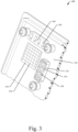
- Fig. 3 illustrates the waveguide antenna 108 with some of the solder 204 and the solder 218 disposed thereon.
- Fig. 3 illustrates the waveguide antenna 108 as it may be configured for attachment to the PCB 106.
- the waveguide antenna 108 has a plurality of apertures 206 in multiple locations. It should be noted that any configuration of apertures 206 (including height from a surface of the waveguide antenna 108) may be used without departing from the scope of this disclosure.
- the solder 204 Surrounding some of the apertures 206 is the solder 204.
- the solder 204 may be disposed in an array around and in between the apertures 206.
- the solder 204 may be attached to waveguide metallic portions 300 disposed on a plastic body 302 of the waveguide antenna 108.
- the waveguide metallic portions 300 (e.g., depositions of the solderable metal) may cover dimples of the plastic body 302 underneath the solder 204 (e.g., a dimple for each solder ball of the solder 204).
- the dimples may be in-molded dimples (e.g., part of the plastic body 302) which enable the solder 204 to stay in a specific location.
- the solder 204 at least partially surrounds the apertures 206 in order to provide shielding after assembly with the PCB 106.
- solder 204 may be disposed on both waveguide metallic portions 300 in the illustrated example; however, some of the solder 204 is not shown (e.g., in the upper waveguide metallic portion 300) to better illustrate the corresponding waveguide metallic portion 300 and the surface to which it is disposed.
- a surface 304 and the solder 218 disposed therethrough are illustrated (e.g., within thermal vias).
- the surface 304 is configured to be proximate the MMIC 212, such that the solder 218 can contact the TIM 216.
- the surface 304 may be flush, raised (as illustrated), or tilted relative to an adjacent surface depending upon the configuration of the MMIC 212 or any other component that can benefit from the heat transfer provided by the solder 218.
- the surface 304 may also be within a cutout or recess formed by the apertures 206 and/or other portions of the plastic body 302 (e.g., for packaging) such that the MMIC 212 may be surrounded (e.g., on a plurality of sides) by the waveguide antenna 108 when the waveguide antenna 108 is assembled to the PCB 106.
- the MMIC 212 (or any other component of the PCB 106) may be at least partially encapsulated by the waveguide antenna 108 when assembled.
- the waveguide antenna 108 may have any number and/or configuration of surfaces 304 for respective components.
- the surface 304 may have a waveguide metallic portion 300 disposed thereon or not.
- a waveguide metallic portion 300 on the surface 304 may enable better heat transfer between portions of the solder 218.
- Fig. 4 is an example method 400 of manufacturing a solderable waveguide antenna.
- a waveguide comprising a plastic body with one or more surfaces configured to mate with corresponding surfaces of a PCB is obtained.
- the plastic body 302 of the waveguide antenna 108 may be obtained with surfaces corresponding to the waveguide metallic portions 300 (but without the waveguide metallic portions 300 disposed thereon).
- a solderable metal is deposited onto the surfaces to create respective metallic portions.
- the metallic portions are solderable features for the solder 204.
- a conductive and/or solderable metal e.g., copper, tin, silver, or an alloy thereof
- PVD Physical Vapor Deposition
- a blocking screen may be used such that locations of the waveguide metallic portions 300 may be controlled (e.g., only around apertures 206, around the surface 304 to electrically seal/shield the MMIC 212, in other locations for structure mounting to the PCB 106).
- the waveguide metallic portions 300 may cover dimples of the plastic body 302 used to house/locate solder.
- solder is deposited onto the metallic portions.
- the solder 204 may be deposited on the waveguide metallic portions 300 within the dimples (e.g., metallurgically bonded).
- the solder 204 may form a ball grid array and be deposited/adhered to the waveguide metallic portions 300 via various known processes.
- the solder 204 may be deposited as 0.2 to 0.5 mm balls and placed at a pitch (e.g., distance from each other).
- the solder 204 may be deposited to the PCB 106, either alternatively or in conjunction, or as part of the assembly process.
- solder may also be deposited within thermal vias of the plastic body (if the waveguide is configured with such).
- the solder 218 may be deposited within the thru holes of the plastic body 302 (e.g., proximate the TIM 216, proximate the MMIC 212).
- Fig. 5 is an example method 500 of attaching a solderable waveguide antenna to a PCB.
- a waveguide comprising one or more waveguide metallic portions and a PCB comprising PCB metallic portions that correspond to the waveguide metallic portions are obtained.
- the waveguide antenna 108 (with the waveguide metallic portions 300) and the PCB 106 (with its metallic portions) may be obtained.
- solder balls are deposited on at least one of the waveguide metallic portions or the PCB metallic portions.
- the solder balls may already be disposed on one or both of the waveguide metallic portions or the PCB metallic portions (e.g., as part of manufacturing the respective parts), thereby obviating step 504.
- the solder 204 may be deposited on the waveguide metallic portions 300 or the PCB metallic portions of the PCB 106.
- the waveguide is arranged proximate the PCB such that the solder balls are in contact with the waveguide metallic portions and the PCB metallic portions.
- the waveguide antenna 108 may be arranged proximate the PCB 106 such that the apertures 206 are aligned with respective RF ports 210.
- the locations of the waveguide metallic portions 300 and the corresponding PCB metallic portions align when the apertures 206 and RF ports 210 are aligned with each other (e.g., due to locations of the respective metallic portions relative to the apertures 206 and RF ports 210).
- heat is applied to the PCB or the waveguide which causes the solder balls to melt, thereby affixing the waveguide to the PCB.
- the arrangement of the PCB and the waveguide may be maintained, such that proper alignment (e.g., aperture to RF port standoff and alignment) is maintained.
- heat may be applied to the PCB 106 or the waveguide antenna 108 effective to melt the solder 204.
- the heat may be a low temp reflow heat, such as 160°C.
- the alignment of the apertures 206 to their respective RF ports 210 may be maintained during the heating process.
- heat is applied to the waveguide effective to melt solder within one or more thermal vias.
- Step 510 may be performed if the waveguide contains the thermal vias.
- heat may be applied to the waveguide antenna 108 effective to melt the solder 218 into the thermal vias of the surface 304 such that the solder 218 is thermally connected to an underlying component (e.g., the MMIC 212 via the TIM 216).
- the solder 218 may then provide a heat transfer path from the underlying component to an external surface (e.g., the external surface 220).
- Example 1 An assembly comprising: a printed circuit board (PCB) comprising: a radio frequency (RF) port; and one or more PCB metallic portions; a waveguide comprising a waveguide channel with an aperture aligned with the RF port of the PCB; and one or more waveguide metallic portions disposed on one or more external surfaces of the waveguide, the waveguide metallic portions corresponding to the PCB metallic portions; and solder disposed between the waveguide metallic portions and the PCB metallic portions.
- PCB printed circuit board
- RF radio frequency
- Example 2 The assembly of example 1, wherein the solder at least partially surrounds the RF port.
- Example 3 The assembly of example 2, wherein the solder is configured to provide electromagnetic interference (EMI) shielding for the RF port.
- EMI electromagnetic interference
- Example 4 The assembly of example 1, wherein: the waveguide is formed of a plastic material; and the waveguide metallic portions are a solderable metal disposed on the plastic material of the external surfaces.
- Example 5 The assembly of example 4, wherein the solderable metal comprises copper, tin, silver, or an alloy thereof.
- Example 6 The assembly of example 4, wherein the waveguide metallic portions comprise depositions of the solderable metal on the plastic material.
- Example 7 The assembly of example 6, wherein the depositions of the solderable metal comprise physical vapor depositions (PVD).
- PVD physical vapor depositions
- Example 8 The assembly of example 1, wherein: the waveguide comprises dimples on the external surfaces; and the waveguide metallic portions and the solder are disposed within the dimples.
- Example 9 The assembly of example 1, wherein: the PCB comprises a monolithic microwave integrated circuit (MN ⁇ C); and the waveguide comprises: a cutout configured to surround the MN ⁇ C; and thru holes disposed within the cutout.
- MN ⁇ C monolithic microwave integrated circuit
- Example 10 The assembly of example 9, further comprising a radome disposed opposite the cutout.
- Example 11 The assembly of example 9, further comprising solder disposed within the thru holes and thermally connected to a thermal interface material (TIM) of the MN ⁇ C.
- TIM thermal interface material
- Example 12 The assembly of example 9, wherein the solder is configured to provide electromagnetic (EMI) shielding for the MN ⁇ C.
- EMI electromagnetic
- Example 13 The assembly of example 1, wherein the solder comprises a tin/bismuth, indium/tin, or other low melting point solder.
- Example 14 A radio frequency (RF) waveguide comprising: a plastic body comprising: a waveguide channel with an aperture configured to mate with a corresponding RF port of a printed circuit board (PCB); and a plurality of dimples on one or more external surfaces of the plastic body; and one or more waveguide metallic portions disposed on the dimples.
- RF radio frequency
- Example 15 A method comprising: obtaining a plastic waveguide comprising a plurality of dimples; depositing solderable metal on the dimples to form one or more waveguide metallic portions; obtaining a printed circuit board (PCB) comprising one or more PCB metallic portions; at least one of: adhering solder balls to the waveguide metallic portions proximate the dimples; or adhering solder balls to the PCB metallic portions; arranging the plastic waveguide proximate the PCB such that the solder balls are in contact with the waveguide metallic portions and the PCB metallic portions; and applying heat to the PCB or the plastic waveguide effective to melt the solder balls and affix the plastic waveguide to the PCB.
- PCB printed circuit board
- Example 16 The method of example 15, wherein depositing the solderable metal on the dimples comprises a physical vapor deposition (PVD) process.
- PVD physical vapor deposition
- Example 17 The method of example 15, wherein: the PCB comprises a monolithic microwave integrated circuit (MN ⁇ C); and arranging the plastic waveguide comprises arranging the plastic waveguide such that the plastic waveguide at least partially surrounds the MN ⁇ C.
- MN ⁇ C monolithic microwave integrated circuit
- Example 18 The method of example 17, wherein: the plastic waveguide comprises a plurality of thru holes; and the method further comprises: placing solder within the thru holes; and applying heat to the plastic waveguide effective to melt the solder.
- Example 19 The method of example 18, wherein: the thru holes are proximate the MN ⁇ C; and applying the heat to the plastic waveguide comprises causing the solder to flow to a thermal interface material (TIM) of the MN ⁇ C.
- TIM thermal interface material
- Example 20 The method of example 15, wherein: one of the waveguide metallic portions or a plurality of the waveguide metallic portions surrounds an aperture of the plastic waveguide; and applying heat to the PCB or the plastic waveguide causes the solder balls to form an electromagnetic interference (EMI) shield for the aperture.
- EMI electromagnetic interference
- Example 21 A method of manufacturing the assembly of any of examples 1-13.
- Example 22 A method of manufacturing the RF waveguide of example 14.
- Example 23 A system configured to perform the method of any of examples 15-20.
- "at least one of: a, b, or c” is intended to cover a, b, c, a-b, a-c, b-c, and a-b-c, as well as any combination with multiples of the same element (e.g., a-a, a-a-a, a-a-b, a-a-c, a-b-b, a-c-c, b-b, b-b-b, b-b-c, c-c, and c-c-c or any other ordering of a, b, and c).
Landscapes
- Engineering & Computer Science (AREA)
- Microelectronics & Electronic Packaging (AREA)
- Manufacturing & Machinery (AREA)
- Physics & Mathematics (AREA)
- Electromagnetism (AREA)
- Waveguide Aerials (AREA)
- Waveguides (AREA)
Applications Claiming Priority (1)
| Application Number | Priority Date | Filing Date | Title |
|---|---|---|---|
| US17/812,770 US12315999B2 (en) | 2022-07-15 | 2022-07-15 | Solderable waveguide antenna |
Publications (1)
| Publication Number | Publication Date |
|---|---|
| EP4311020A1 true EP4311020A1 (de) | 2024-01-24 |
Family
ID=85726517
Family Applications (1)
| Application Number | Title | Priority Date | Filing Date |
|---|---|---|---|
| EP23163661.4A Pending EP4311020A1 (de) | 2022-07-15 | 2023-03-23 | Lötbare wellenleiterantenne |
Country Status (3)
| Country | Link |
|---|---|
| US (2) | US12315999B2 (de) |
| EP (1) | EP4311020A1 (de) |
| CN (1) | CN117410694A (de) |
Citations (6)
| Publication number | Priority date | Publication date | Assignee | Title |
|---|---|---|---|---|
| US5400220A (en) * | 1994-05-18 | 1995-03-21 | Dell Usa, L.P. | Mechanical printed circuit board and ball grid array interconnect apparatus |
| US6340113B1 (en) * | 1995-10-06 | 2002-01-22 | Donald H. Avery | Soldering methods and compositions |
| US20090168367A1 (en) * | 2007-12-27 | 2009-07-02 | Shinko Electric Industries Co., Ltd. | Electronic apparatus |
| US20200343612A1 (en) * | 2019-04-29 | 2020-10-29 | Aptiv Technologies Limited | Wave guide launcher |
| DE102020211254A1 (de) * | 2020-09-08 | 2022-03-10 | Conti Temic Microelectronic Gmbh | Radarsystem zur Umgebungserfassung mit einer Wellenleiterantenne gebildet aus einer Platine und einem Formteil |
| US20220109247A1 (en) * | 2020-10-02 | 2022-04-07 | Aptiv Technologies Limited | Plastic Air-Waveguide Antenna with Conductive Particles |
Family Cites Families (108)
| Publication number | Priority date | Publication date | Assignee | Title |
|---|---|---|---|---|
| US3462713A (en) | 1967-07-19 | 1969-08-19 | Bell Telephone Labor Inc | Waveguide-stripline transducer |
| US3579149A (en) | 1969-12-08 | 1971-05-18 | Westinghouse Electric Corp | Waveguide to stripline transition means |
| NL7609903A (nl) | 1976-09-07 | 1978-03-09 | Philips Nv | Microgolfinrichting voor het omzetten van een golfpijp- in een microstripgeleiderstructuur. |
| US4453142A (en) | 1981-11-02 | 1984-06-05 | Motorola Inc. | Microstrip to waveguide transition |
| US4562416A (en) | 1984-05-31 | 1985-12-31 | Sanders Associates, Inc. | Transition from stripline to waveguide |
| TW212252B (de) | 1992-05-01 | 1993-09-01 | Martin Marietta Corp | |
| US5432487A (en) | 1994-03-28 | 1995-07-11 | Motorola, Inc. | MMIC differential phase shifter |
| US5986527A (en) | 1995-03-28 | 1999-11-16 | Murata Manufacturing Co., Ltd. | Planar dielectric line and integrated circuit using the same line |
| JP3366552B2 (ja) | 1997-04-22 | 2003-01-14 | 京セラ株式会社 | 誘電体導波管線路およびそれを具備する多層配線基板 |
| CA2292064C (en) | 1998-12-25 | 2003-08-19 | Murata Manufacturing Co., Ltd. | Line transition device between dielectric waveguide and waveguide, and oscillator and transmitter using the same |
| US6590477B1 (en) | 1999-10-29 | 2003-07-08 | Fci Americas Technology, Inc. | Waveguides and backplane systems with at least one mode suppression gap |
| AU2000277887A1 (en) | 2000-10-18 | 2002-04-29 | Nokia Corporation | Waveguide to stripline transition |
| EP1346431A1 (de) | 2000-12-21 | 2003-09-24 | Paratek Microwave, Inc. | Hohlleiter-mikrostreifenleiterübergang |
| CN1316858C (zh) * | 2001-04-27 | 2007-05-16 | 日本电气株式会社 | 高频电路基板及其制造方法 |
| US6967347B2 (en) | 2001-05-21 | 2005-11-22 | The Regents Of The University Of Colorado | Terahertz interconnect system and applications |
| JP2003289201A (ja) | 2002-03-28 | 2003-10-10 | Anritsu Corp | ポスト壁導波管と空洞導波管の接続変換構造 |
| US7098070B2 (en) | 2004-11-16 | 2006-08-29 | International Business Machines Corporation | Device and method for fabricating double-sided SOI wafer scale package with through via connections |
| CN2796131Y (zh) | 2005-05-30 | 2006-07-12 | 东南大学 | 多层基片集成波导椭圆响应滤波器 |
| WO2007114391A1 (ja) | 2006-03-31 | 2007-10-11 | Kyocera Corporation | 誘電体導波路デバイス、これを備える移相器、高周波スイッチおよび減衰器、ならびに高周波送信器、高周波受信器、高周波送受信器およびレーダ装置、アレイアンテナ装置、誘電体導波路デバイスの製造方法 |
| CN101915957B (zh) | 2006-06-12 | 2012-12-12 | 加利福尼亚太平洋生物科学公司 | 实施分析反应的基材 |
| KR100846872B1 (ko) | 2006-11-17 | 2008-07-16 | 한국전자통신연구원 | 유전체 도파관 대 전송선의 밀리미터파 천이 장치 |
| JP4365852B2 (ja) | 2006-11-30 | 2009-11-18 | 株式会社日立製作所 | 導波管構造 |
| EP1936741A1 (de) | 2006-12-22 | 2008-06-25 | Sony Deutschland GmbH | Flexible substratintegrierte Wellenleiter |
| US8231284B2 (en) | 2007-03-26 | 2012-07-31 | International Business Machines Corporation | Ultra-high bandwidth, multiple-channel full-duplex, single-chip CMOS optical transceiver |
| US7768457B2 (en) | 2007-06-22 | 2010-08-03 | Vubiq, Inc. | Integrated antenna and chip package and method of manufacturing thereof |
| US8159316B2 (en) | 2007-12-28 | 2012-04-17 | Kyocera Corporation | High-frequency transmission line connection structure, circuit board, high-frequency module, and radar device |
| CA2629035A1 (en) | 2008-03-27 | 2009-09-27 | Her Majesty The Queen In Right Of Canada, As Represented By The Minister Of Industry, Through The Communications Research Centre Canada | Waveguide filter with broad stopband based on sugstrate integrated waveguide scheme |
| JP5172481B2 (ja) | 2008-06-05 | 2013-03-27 | 株式会社東芝 | ポスト壁導波路によるショートスロット方向性結合器とこれを用いたバトラーマトリクス及び車載レーダアンテナ |
| WO2010026990A1 (ja) * | 2008-09-05 | 2010-03-11 | 三菱電機株式会社 | 高周波回路パッケージおよびセンサモジュール |
| JP5044536B2 (ja) | 2008-12-12 | 2012-10-10 | 株式会社東芝 | 導波管・伝送線路変換器、およびアンテナ装置 |
| US7990237B2 (en) | 2009-01-16 | 2011-08-02 | Toyota Motor Engineering & Manufacturing North America, Inc. | System and method for improving performance of coplanar waveguide bends at mm-wave frequencies |
| US8089327B2 (en) | 2009-03-09 | 2012-01-03 | Toyota Motor Engineering & Manufacturing North America, Inc. | Waveguide to plural microstrip transition |
| KR101327375B1 (ko) | 2009-03-31 | 2013-11-08 | 쿄세라 코포레이션 | 도파 구조체, 도파 구조체를 포함하는 고주파 모듈, 및 레이더 장치 |
| CN201383535Y (zh) | 2009-04-01 | 2010-01-13 | 惠州市硕贝德通讯科技有限公司 | 一种矩形波导-基片集成波导信号转换及功率分配器 |
| WO2010127709A1 (en) | 2009-05-08 | 2010-11-11 | Telefonaktiebolaget L M Ericsson (Publ) | A transition from a chip to a waveguide port |
| US9088058B2 (en) | 2009-08-19 | 2015-07-21 | Vubiq Networks, Inc. | Waveguide interface with a launch transducer and a circular interface plate |
| US8912858B2 (en) | 2009-09-08 | 2014-12-16 | Siklu Communication ltd. | Interfacing between an integrated circuit and a waveguide through a cavity located in a soft laminate |
| FR2953651B1 (fr) | 2009-12-07 | 2012-01-20 | Eads Defence & Security Sys | Dispositif de transition hyperfrequence entre une ligne a micro-ruban et un guide d'onde rectangulaire |
| ES2612488T3 (es) | 2010-03-10 | 2017-05-17 | Huawei Technologies Co., Ltd. | Acoplador de microcinta |
| US8674885B2 (en) | 2010-08-31 | 2014-03-18 | Siklu Communication ltd. | Systems for interfacing waveguide antenna feeds with printed circuit boards |
| US9774076B2 (en) | 2010-08-31 | 2017-09-26 | Siklu Communication ltd. | Compact millimeter-wave radio systems and methods |
| US9398694B2 (en) | 2011-01-18 | 2016-07-19 | Sony Corporation | Method of manufacturing a package for embedding one or more electronic components |
| KR101761920B1 (ko) | 2011-02-16 | 2017-07-26 | 삼성전기주식회사 | 유전체 도파관 안테나 |
| EP2500978B1 (de) | 2011-03-17 | 2013-07-10 | Sivers Ima AB | Wellenleiterübergang |
| GB2489950A (en) | 2011-04-12 | 2012-10-17 | Filtronic Plc | A substrate integrated waveguide (SIW) to air filled waveguide transition comprising a tapered dielectric layer |
| US8665078B2 (en) | 2011-07-25 | 2014-03-04 | Ford Global Technologies | Width calibration of lane departure warning system |
| US9147924B2 (en) | 2011-09-02 | 2015-09-29 | The United States Of America As Represented By The Secretary Of The Army | Waveguide to co-planar-waveguide (CPW) transition |
| EP2862230B1 (de) | 2012-06-18 | 2016-08-10 | Huawei Technologies Co., Ltd. | Hohlleiterstruktur mit richtkoppler und verfahren |
| JP5694246B2 (ja) | 2012-07-13 | 2015-04-01 | 株式会社東芝 | 導波管接続構造、アンテナ装置およびレーダ装置 |
| US20140106684A1 (en) | 2012-10-15 | 2014-04-17 | Qualcomm Mems Technologies, Inc. | Transparent antennas on a display device |
| JP2016503245A (ja) | 2013-01-10 | 2016-02-01 | 日本電気株式会社 | 平面伝送線路および導波管の間の広帯域変換器 |
| EP2979321B1 (de) | 2013-03-24 | 2017-01-11 | Telefonaktiebolaget LM Ericsson (publ) | Übergang zwischen einer siw und einer wellenleiterschnittstelle |
| CN103515682B (zh) | 2013-07-24 | 2015-07-29 | 中国电子科技集团公司第五十五研究所 | 多层阶梯式基片集成波导实现微带至波导的垂直过渡结构 |
| WO2015013927A1 (zh) | 2013-07-31 | 2015-02-05 | 华为技术有限公司 | 一种天线 |
| EP2843758A1 (de) | 2013-08-27 | 2015-03-04 | Microelectronics Technology Inc. | Mehrlagige Leiterplatte mit Wellenleiter zu einer Mikrostreifen-Übergangsstruktur |
| EP2848488B2 (de) | 2013-09-12 | 2022-04-13 | Volvo Car Corporation | Verfahren und Einrichtung zur Übergabewarnung in einem Fahrzeug mit autonomer Fahrfähigkeit |
| US10014566B2 (en) | 2013-10-01 | 2018-07-03 | Sony Semiconductor Solutions Corporation | Connector apparatus and communication system |
| US9059490B2 (en) | 2013-10-08 | 2015-06-16 | Blackberry Limited | 60 GHz integrated circuit to printed circuit board transitions |
| CN105830470A (zh) | 2013-11-22 | 2016-08-03 | 高通股份有限公司 | 用于基于用车辆内的多个移动计算设备提供的偏好来配置车辆的内部的系统和方法 |
| WO2015076009A1 (ja) | 2013-11-25 | 2015-05-28 | 株式会社村田製作所 | 高周波装置及び該高周波装置の制御方法 |
| JP6269127B2 (ja) | 2014-02-07 | 2018-01-31 | 富士通株式会社 | 高周波モジュール及びその製造方法 |
| US9515385B2 (en) | 2014-03-18 | 2016-12-06 | Peraso Technologies Inc. | Coplanar waveguide implementing launcher and waveguide channel section in IC package substrate |
| US9632251B2 (en) | 2014-04-02 | 2017-04-25 | International Business Machines Corporation | Integration of photonic, electronic, and sensor devices with SOI VLSI microprocessor technology |
| US9779331B2 (en) | 2014-04-24 | 2017-10-03 | Conduent Business Services, Llc | Method and system for partial occlusion handling in vehicle tracking using deformable parts model |
| DE102014209874A1 (de) | 2014-05-23 | 2015-11-26 | Conti Temic Microelectronic Gmbh | Steuergerät für ein Fahrzeug mit einem einen Drucksensor aufweisenden Gehäuse |
| US10103447B2 (en) | 2014-06-13 | 2018-10-16 | Nxp Usa, Inc. | Integrated circuit package with radio frequency coupling structure |
| US9620841B2 (en) | 2014-06-13 | 2017-04-11 | Nxp Usa, Inc. | Radio frequency coupling structure |
| US9517668B2 (en) | 2014-07-28 | 2016-12-13 | Ford Global Technologies, Llc | Hitch angle warning system and method |
| US9583811B2 (en) | 2014-08-07 | 2017-02-28 | Infineon Technologies Ag | Transition between a plastic waveguide and a semiconductor chip, where the semiconductor chip is embedded and encapsulated within a mold compound |
| US9571711B2 (en) | 2014-09-08 | 2017-02-14 | Imperx, Inc. | Illumination apparatus with integrated power and secondary illumination provisions |
| KR101621480B1 (ko) | 2014-10-16 | 2016-05-16 | 현대모비스 주식회사 | 도파관 대 유전체 도파관의 천이 구조 |
| US9666930B2 (en) | 2014-10-23 | 2017-05-30 | Nxp Usa, Inc. | Interface between a semiconductor die and a waveguide, where the interface is covered by a molding compound |
| DE112015005575T5 (de) | 2014-12-12 | 2017-09-28 | Sony Corporation | Mikrowellenantennenvorrichtung, einheit und herstellungsverfahren |
| US20160276308A1 (en) * | 2015-03-17 | 2016-09-22 | Samsung Electronics Co., Ltd. | Thermally enhanced package-on-package structure |
| US9537199B2 (en) | 2015-03-19 | 2017-01-03 | International Business Machines Corporation | Package structure having an integrated waveguide configured to communicate between first and second integrated circuit chips |
| US10109604B2 (en) | 2015-03-30 | 2018-10-23 | Sony Corporation | Package with embedded electronic components and a waveguide cavity through the package cover, antenna apparatus including package, and method of manufacturing the same |
| KR101689353B1 (ko) | 2015-04-13 | 2016-12-23 | 성균관대학교산학협력단 | 실리콘 밀리미터파 칩용 칩상 도파관 급전기 및 급전 방법 및, 이를 이용한 다중 입출력 밀리미터파 송수신 장치 |
| CN104900956A (zh) | 2015-05-06 | 2015-09-09 | 东南大学 | 一种波导到基片集成波导的转换装置 |
| US10083923B2 (en) | 2015-09-21 | 2018-09-25 | Intel Corporation | Platform with thermally stable wireless interconnects |
| IL241951B (en) | 2015-10-07 | 2018-04-30 | Israel Aerospace Ind Ltd | Galvo components, production methods and their organizations |
| CN105680133B (zh) | 2016-01-11 | 2018-08-10 | 中国电子科技集团公司第十研究所 | 基片集成脊波导板间垂直互联电路结构 |
| CN108475833A (zh) | 2016-01-20 | 2018-08-31 | 索尼公司 | 连接器模块、通信电路板和电子装置 |
| CN105609909A (zh) | 2016-03-08 | 2016-05-25 | 电子科技大学 | 一种用于Ka波段矩形波导转基片集成波导的装置 |
| TWI610492B (zh) | 2016-03-31 | 2018-01-01 | 為昇科科技股份有限公司 | 雙槽孔基板導波天線單元及其陣列模組 |
| CN207587944U (zh) | 2016-06-29 | 2018-07-06 | 日本电产株式会社 | 波导装置模块以及微波模块 |
| CN105958167B (zh) | 2016-07-01 | 2019-03-05 | 北京交通大学 | 垂直基片集成波导及包括该波导的垂直连接结构 |
| KR101963936B1 (ko) | 2016-11-08 | 2019-07-31 | 한국과학기술원 | 전자파 신호 송수신 안테나 및 em-터널이 내장된 구조를 갖는 인쇄회로기판 및 그 제작 방법 |
| US9935065B1 (en) | 2016-12-21 | 2018-04-03 | Infineon Technologies Ag | Radio frequency device packages and methods of formation thereof |
| US10468736B2 (en) | 2017-02-08 | 2019-11-05 | Aptiv Technologies Limited | Radar assembly with ultra wide band waveguide to substrate integrated waveguide transition |
| EP3364457A1 (de) | 2017-02-15 | 2018-08-22 | Nxp B.V. | Integriertes schaltungsgehäuse mit antenne |
| US10333226B2 (en) | 2017-03-10 | 2019-06-25 | Speedlink Technology Inc. | Waveguide antenna with cavity |
| US10317459B2 (en) | 2017-04-03 | 2019-06-11 | Nvidia Corporation | Multi-chip package with selection logic and debug ports for testing inter-chip communications |
| US10129388B1 (en) | 2017-05-01 | 2018-11-13 | Verizon Patent And Licensing Inc. | Systems and methods for restricting operation of a mobile device while operating a vehicle |
| US10530047B2 (en) | 2017-05-24 | 2020-01-07 | Waymo Llc | Broadband waveguide launch designs on single layer PCB |
| DE102017111319A1 (de) | 2017-05-24 | 2018-11-29 | Miele & Cie. Kg | Einrichtung zur Erzeugung und Transmission von Hochfrequenzwellen (HF-Wellen) |
| CN108987866A (zh) | 2017-06-05 | 2018-12-11 | 日本电产株式会社 | 波导装置以及具有该波导装置的天线装置 |
| DE102018115610A1 (de) | 2017-06-30 | 2019-01-03 | Nidec Corporation | Wellenleitervorrichtungsmodul, Mikrowellenmodul, Radarvorrichtung und Radarsystem |
| US11183751B2 (en) | 2017-09-20 | 2021-11-23 | Aptiv Technologies Limited | Antenna device with direct differential input useable on an automated vehicle |
| US20210356504A1 (en) | 2018-10-19 | 2021-11-18 | Gapwaves Ab | Contactless antenna measurement device |
| DE102019200893B4 (de) | 2019-01-21 | 2023-06-15 | Infineon Technologies Ag | Verfahren zum Erzeugen eines Hohlleiters, Schaltungsvorrichtung und Radarsystem |
| CN209389219U (zh) | 2019-02-25 | 2019-09-13 | 贵州航天电子科技有限公司 | 一种适用于增材制造的波导缝隙阵列天线结构 |
| US10775573B1 (en) | 2019-04-03 | 2020-09-15 | International Business Machines Corporation | Embedding mirror with metal particle coating |
| EP3793336A1 (de) * | 2019-09-10 | 2021-03-17 | AT & S Austria Technologie & Systemtechnik Aktiengesellschaft | Verbindungsanordnung, komponententräger und verfahren zur formung einer komponententrägerstruktur |
| DE102020101293A1 (de) * | 2020-01-21 | 2021-07-22 | Infineon Technologies Ag | Hochfrequenz-vorrichtung mit halbleitervorrichtung und wellenleiter-bauteil |
| US11664567B2 (en) * | 2020-11-30 | 2023-05-30 | Nxp B.V. | Hollow waveguide assembly formed by affixing first and second substrates to form a cavity therein and having a conductive layer covering the cavity |
| DE102021102228A1 (de) * | 2021-02-01 | 2022-08-04 | Infineon Technologies Ag | Hochfrequenz-Vorrichtungen und Verfahren zur Herstellung von Hochfrequenz-Vorrichtungen |
| DE102022203285A1 (de) * | 2022-04-01 | 2023-10-05 | Robert Bosch Gesellschaft mit beschränkter Haftung | Radarsystem |
| US11963291B2 (en) * | 2022-04-21 | 2024-04-16 | Nxp B.V. | Efficient wave guide transition between package and PCB using solder wall |
-
2022
- 2022-07-15 US US17/812,770 patent/US12315999B2/en active Active
-
2023
- 2023-03-23 EP EP23163661.4A patent/EP4311020A1/de active Pending
- 2023-05-30 CN CN202310629015.3A patent/CN117410694A/zh active Pending
-
2025
- 2025-05-01 US US19/196,015 patent/US20250260170A1/en active Pending
Patent Citations (6)
| Publication number | Priority date | Publication date | Assignee | Title |
|---|---|---|---|---|
| US5400220A (en) * | 1994-05-18 | 1995-03-21 | Dell Usa, L.P. | Mechanical printed circuit board and ball grid array interconnect apparatus |
| US6340113B1 (en) * | 1995-10-06 | 2002-01-22 | Donald H. Avery | Soldering methods and compositions |
| US20090168367A1 (en) * | 2007-12-27 | 2009-07-02 | Shinko Electric Industries Co., Ltd. | Electronic apparatus |
| US20200343612A1 (en) * | 2019-04-29 | 2020-10-29 | Aptiv Technologies Limited | Wave guide launcher |
| DE102020211254A1 (de) * | 2020-09-08 | 2022-03-10 | Conti Temic Microelectronic Gmbh | Radarsystem zur Umgebungserfassung mit einer Wellenleiterantenne gebildet aus einer Platine und einem Formteil |
| US20220109247A1 (en) * | 2020-10-02 | 2022-04-07 | Aptiv Technologies Limited | Plastic Air-Waveguide Antenna with Conductive Particles |
Also Published As
| Publication number | Publication date |
|---|---|
| CN117410694A (zh) | 2024-01-16 |
| US20250260170A1 (en) | 2025-08-14 |
| US20240022001A1 (en) | 2024-01-18 |
| US12315999B2 (en) | 2025-05-27 |
Similar Documents
| Publication | Publication Date | Title |
|---|---|---|
| CA2439065C (en) | Removable electromagnetic interference shield | |
| CA2424885C (en) | Methods of manufacturing a printed circuit board shielded against interfering radiation | |
| US10319685B2 (en) | EMI shielded integrated circuit packages and methods of making the same | |
| EP2248398B1 (de) | System und verfahren zur kapselung integrierter wellenleiter | |
| AU2002250184A1 (en) | Removable electromagnetic interference shield | |
| US7971350B2 (en) | Method of providing a RF shield of an electronic device | |
| US20120218727A1 (en) | Shield case for emi shielding | |
| US20200043866A1 (en) | Module | |
| US20020075664A1 (en) | Method and apparatus for providing electromagnetic shielding | |
| JPWO2011118544A1 (ja) | 無線モジュール及びその製造方法 | |
| EP1671524B1 (de) | Elektrische schaltungsvorrichtung und verfahren zu ihrem zusammenbau | |
| EP1668697B1 (de) | Elektrische schaltungsvorrichtung und verfahren zu ihrem zusammenbau | |
| EP4311020A1 (de) | Lötbare wellenleiterantenne | |
| US20070119904A1 (en) | Electrical circuit apparatus | |
| EP2704536A1 (de) | Verfahren zum Herstellen eines Schalttafelsystems | |
| US20050185383A1 (en) | Power amplifier module assembly | |
| US10375865B2 (en) | Mechanically attached edge shield | |
| US11184049B2 (en) | Systems and methods for signal isolation in radio frequency circuit boards |
Legal Events
| Date | Code | Title | Description |
|---|---|---|---|
| PUAI | Public reference made under article 153(3) epc to a published international application that has entered the european phase |
Free format text: ORIGINAL CODE: 0009012 |
|
| STAA | Information on the status of an ep patent application or granted ep patent |
Free format text: STATUS: THE APPLICATION HAS BEEN PUBLISHED |
|
| AK | Designated contracting states |
Kind code of ref document: A1 Designated state(s): AL AT BE BG CH CY CZ DE DK EE ES FI FR GB GR HR HU IE IS IT LI LT LU LV MC ME MK MT NL NO PL PT RO RS SE SI SK SM TR |
|
| RAP1 | Party data changed (applicant data changed or rights of an application transferred) |
Owner name: APTIV TECHNOLOGIES AG |
|
| STAA | Information on the status of an ep patent application or granted ep patent |
Free format text: STATUS: REQUEST FOR EXAMINATION WAS MADE |
|
| 17P | Request for examination filed |
Effective date: 20240712 |
|
| RBV | Designated contracting states (corrected) |
Designated state(s): AL AT BE BG CH CY CZ DE DK EE ES FI FR GB GR HR HU IE IS IT LI LT LU LV MC ME MK MT NL NO PL PT RO RS SE SI SK SM TR |
|
| RAP3 | Party data changed (applicant data changed or rights of an application transferred) |
Owner name: APTIV TECHNOLOGIES AG |
|
| STAA | Information on the status of an ep patent application or granted ep patent |
Free format text: STATUS: EXAMINATION IS IN PROGRESS |
|
| 17Q | First examination report despatched |
Effective date: 20251205 |