EP4311106A1 - Amplificateur de puissance numérique et système de communication - Google Patents
Amplificateur de puissance numérique et système de communication Download PDFInfo
- Publication number
- EP4311106A1 EP4311106A1 EP21936811.5A EP21936811A EP4311106A1 EP 4311106 A1 EP4311106 A1 EP 4311106A1 EP 21936811 A EP21936811 A EP 21936811A EP 4311106 A1 EP4311106 A1 EP 4311106A1
- Authority
- EP
- European Patent Office
- Prior art keywords
- transistor
- signal
- quantization
- voltage range
- operating voltage
- Prior art date
- Legal status (The legal status is an assumption and is not a legal conclusion. Google has not performed a legal analysis and makes no representation as to the accuracy of the status listed.)
- Pending
Links
- 238000004891 communication Methods 0.000 title claims abstract description 40
- 238000013139 quantization Methods 0.000 claims abstract description 274
- 238000012545 processing Methods 0.000 claims abstract description 40
- 230000003321 amplification Effects 0.000 claims description 70
- 238000003199 nucleic acid amplification method Methods 0.000 claims description 70
- 239000003990 capacitor Substances 0.000 claims description 34
- 230000003595 spectral effect Effects 0.000 claims description 16
- 230000015654 memory Effects 0.000 description 26
- 238000010586 diagram Methods 0.000 description 21
- 238000005516 engineering process Methods 0.000 description 12
- 238000000034 method Methods 0.000 description 10
- 238000006243 chemical reaction Methods 0.000 description 9
- 238000013461 design Methods 0.000 description 7
- 230000008569 process Effects 0.000 description 5
- 230000005540 biological transmission Effects 0.000 description 4
- 230000007423 decrease Effects 0.000 description 4
- 230000007774 longterm Effects 0.000 description 4
- 230000001174 ascending effect Effects 0.000 description 3
- 238000012986 modification Methods 0.000 description 3
- 230000004048 modification Effects 0.000 description 3
- 230000003190 augmentative effect Effects 0.000 description 2
- 238000001914 filtration Methods 0.000 description 2
- 230000006870 function Effects 0.000 description 2
- 230000008054 signal transmission Effects 0.000 description 2
- 238000001228 spectrum Methods 0.000 description 2
- 230000003068 static effect Effects 0.000 description 2
- 238000001356 surgical procedure Methods 0.000 description 2
- 239000013598 vector Substances 0.000 description 2
- 239000010755 BS 2869 Class G Substances 0.000 description 1
- 101710082751 Carboxypeptidase S1 homolog A Proteins 0.000 description 1
- 101001076732 Homo sapiens RNA-binding protein 27 Proteins 0.000 description 1
- 102100025873 RNA-binding protein 27 Human genes 0.000 description 1
- 241001125929 Trisopterus luscus Species 0.000 description 1
- 230000015572 biosynthetic process Effects 0.000 description 1
- 230000008859 change Effects 0.000 description 1
- 230000009977 dual effect Effects 0.000 description 1
- 230000000694 effects Effects 0.000 description 1
- 230000005611 electricity Effects 0.000 description 1
- 230000008571 general function Effects 0.000 description 1
- 230000017525 heat dissipation Effects 0.000 description 1
- 238000012872 hydroxylapatite chromatography Methods 0.000 description 1
- 230000010354 integration Effects 0.000 description 1
- 238000010295 mobile communication Methods 0.000 description 1
- 230000003287 optical effect Effects 0.000 description 1
- 238000005070 sampling Methods 0.000 description 1
- 238000003786 synthesis reaction Methods 0.000 description 1
- 230000009466 transformation Effects 0.000 description 1
Images






Classifications
-
- H—ELECTRICITY
- H03—ELECTRONIC CIRCUITRY
- H03F—AMPLIFIERS
- H03F1/00—Details of amplifiers with only discharge tubes, only semiconductor devices or only unspecified devices as amplifying elements
- H03F1/56—Modifications of input or output impedances, not otherwise provided for
-
- H—ELECTRICITY
- H03—ELECTRONIC CIRCUITRY
- H03F—AMPLIFIERS
- H03F1/00—Details of amplifiers with only discharge tubes, only semiconductor devices or only unspecified devices as amplifying elements
- H03F1/02—Modifications of amplifiers to raise the efficiency, e.g. gliding Class A stages, use of an auxiliary oscillation
- H03F1/0205—Modifications of amplifiers to raise the efficiency, e.g. gliding Class A stages, use of an auxiliary oscillation in transistor amplifiers
- H03F1/0277—Selecting one or more amplifiers from a plurality of amplifiers
-
- H—ELECTRICITY
- H03—ELECTRONIC CIRCUITRY
- H03F—AMPLIFIERS
- H03F1/00—Details of amplifiers with only discharge tubes, only semiconductor devices or only unspecified devices as amplifying elements
- H03F1/02—Modifications of amplifiers to raise the efficiency, e.g. gliding Class A stages, use of an auxiliary oscillation
- H03F1/0205—Modifications of amplifiers to raise the efficiency, e.g. gliding Class A stages, use of an auxiliary oscillation in transistor amplifiers
- H03F1/0288—Modifications of amplifiers to raise the efficiency, e.g. gliding Class A stages, use of an auxiliary oscillation in transistor amplifiers using a main and one or several auxiliary peaking amplifiers whereby the load is connected to the main amplifier using an impedance inverter, e.g. Doherty amplifiers
-
- H—ELECTRICITY
- H03—ELECTRONIC CIRCUITRY
- H03F—AMPLIFIERS
- H03F3/00—Amplifiers with only discharge tubes or only semiconductor devices as amplifying elements
- H03F3/189—High-frequency amplifiers, e.g. radio frequency amplifiers
- H03F3/19—High-frequency amplifiers, e.g. radio frequency amplifiers with semiconductor devices only
- H03F3/195—High-frequency amplifiers, e.g. radio frequency amplifiers with semiconductor devices only in integrated circuits
-
- H—ELECTRICITY
- H03—ELECTRONIC CIRCUITRY
- H03F—AMPLIFIERS
- H03F3/00—Amplifiers with only discharge tubes or only semiconductor devices as amplifying elements
- H03F3/20—Power amplifiers, e.g. Class B amplifiers, Class C amplifiers
- H03F3/21—Power amplifiers, e.g. Class B amplifiers, Class C amplifiers with semiconductor devices only
- H03F3/213—Power amplifiers, e.g. Class B amplifiers, Class C amplifiers with semiconductor devices only in integrated circuits
-
- H—ELECTRICITY
- H03—ELECTRONIC CIRCUITRY
- H03F—AMPLIFIERS
- H03F3/00—Amplifiers with only discharge tubes or only semiconductor devices as amplifying elements
- H03F3/20—Power amplifiers, e.g. Class B amplifiers, Class C amplifiers
- H03F3/21—Power amplifiers, e.g. Class B amplifiers, Class C amplifiers with semiconductor devices only
- H03F3/217—Class D power amplifiers; Switching amplifiers
- H03F3/2175—Class D power amplifiers; Switching amplifiers using analogue-digital or digital-analogue conversion
-
- H—ELECTRICITY
- H03—ELECTRONIC CIRCUITRY
- H03F—AMPLIFIERS
- H03F3/00—Amplifiers with only discharge tubes or only semiconductor devices as amplifying elements
- H03F3/20—Power amplifiers, e.g. Class B amplifiers, Class C amplifiers
- H03F3/24—Power amplifiers, e.g. Class B amplifiers, Class C amplifiers of transmitter output stages
- H03F3/245—Power amplifiers, e.g. Class B amplifiers, Class C amplifiers of transmitter output stages with semiconductor devices only
-
- H—ELECTRICITY
- H04—ELECTRIC COMMUNICATION TECHNIQUE
- H04B—TRANSMISSION
- H04B1/00—Details of transmission systems, not covered by a single one of groups H04B3/00 - H04B13/00; Details of transmission systems not characterised by the medium used for transmission
- H04B1/02—Transmitters
- H04B1/04—Circuits
-
- H—ELECTRICITY
- H03—ELECTRONIC CIRCUITRY
- H03F—AMPLIFIERS
- H03F2200/00—Indexing scheme relating to amplifiers
- H03F2200/294—Indexing scheme relating to amplifiers the amplifier being a low noise amplifier [LNA]
-
- H—ELECTRICITY
- H03—ELECTRONIC CIRCUITRY
- H03F—AMPLIFIERS
- H03F2200/00—Indexing scheme relating to amplifiers
- H03F2200/451—Indexing scheme relating to amplifiers the amplifier being a radio frequency amplifier
-
- H—ELECTRICITY
- H03—ELECTRONIC CIRCUITRY
- H03M—CODING; DECODING; CODE CONVERSION IN GENERAL
- H03M1/00—Analogue/digital conversion; Digital/analogue conversion
- H03M1/66—Digital/analogue converters
- H03M1/74—Simultaneous conversion
- H03M1/80—Simultaneous conversion using weighted impedances
- H03M1/802—Simultaneous conversion using weighted impedances using capacitors, e.g. neuron-mos transistors, charge coupled devices
-
- H—ELECTRICITY
- H04—ELECTRIC COMMUNICATION TECHNIQUE
- H04B—TRANSMISSION
- H04B1/00—Details of transmission systems, not covered by a single one of groups H04B3/00 - H04B13/00; Details of transmission systems not characterised by the medium used for transmission
- H04B1/02—Transmitters
- H04B1/04—Circuits
- H04B2001/0408—Circuits with power amplifiers
- H04B2001/045—Circuits with power amplifiers with means for improving efficiency
-
- Y—GENERAL TAGGING OF NEW TECHNOLOGICAL DEVELOPMENTS; GENERAL TAGGING OF CROSS-SECTIONAL TECHNOLOGIES SPANNING OVER SEVERAL SECTIONS OF THE IPC; TECHNICAL SUBJECTS COVERED BY FORMER USPC CROSS-REFERENCE ART COLLECTIONS [XRACs] AND DIGESTS
- Y02—TECHNOLOGIES OR APPLICATIONS FOR MITIGATION OR ADAPTATION AGAINST CLIMATE CHANGE
- Y02D—CLIMATE CHANGE MITIGATION TECHNOLOGIES IN INFORMATION AND COMMUNICATION TECHNOLOGIES [ICT], I.E. INFORMATION AND COMMUNICATION TECHNOLOGIES AIMING AT THE REDUCTION OF THEIR OWN ENERGY USE
- Y02D30/00—Reducing energy consumption in communication networks
- Y02D30/70—Reducing energy consumption in communication networks in wireless communication networks
Definitions
- This application relates to the field of communication technologies, and in particular, to a digital power amplifier and a communication system.
- modulation signals of different standards are used in wireless communication, for example, orthogonal frequency division multiplexing (orthogonal frequency division multiplexing, OFMA), code-division multiple access (code-division multiple access, CDMA), and time division multiple access (time division multiple access, TDMA).
- OFMA orthogonal frequency division multiplexing
- CDMA code-division multiple access
- TDMA time division multiple access
- signals of these standards have different peak-to-average ratios (peak-to-average power ratio, PAPR).
- a peak-to-average ratio of an orthogonal frequency division multiplexing (orthogonal frequency division multiplexing, OFDM) signal is 10 dB to 12 dB.
- a power amplifier (power amplifier, PA) is required to have a high linearity feature.
- a signal with a high peak-to-average power ratio has a higher requirement on the power amplifier in a base station.
- an amplifier Based on a feature of a power tube, an amplifier has a linear dynamic range. Within this range, output power of the amplifier increases linearly with input power. As the input power continues to increase, the amplifier gradually enters a saturation region, and a power gain starts to decrease.
- a power back-off method may be used, so that the PA backs off to a linear operation region.
- a digital PA uses, with reference to a high efficiency feature of a switching PA, a plurality of bits to quantize an input analog signal, to obtain a digital signal of a corresponding quantity of bits, and then inputs the digital signal to the DPA for power amplification, thereby effectively improving the linearity of the DPA.
- a quantity of transistors in the DPA and a quantity of quantization bits of a signal increase exponentially. For example, to obtain 15-bit DPA quantization precision, the quantity of transistors reaches thousands, resulting in relatively high costs and complexity of the power amplifier.
- This application provides a digital power amplifier and a communication system, to reduce a quantity of transistors in the digital power amplifier while ensuring quantization precision of the digital power amplifier by designing the transistors in the digital power amplifier, thereby reducing overheads of the power amplifier and improving overall performance of the power amplifier.
- this application provides a digital power amplifier DPA, including a decoder and N transistor sets.
- the decoder includes an input end and N groups of output ends, the input end of the decoder is connected to a baseband processing unit, the N groups of output ends of the decoder are respectively connected to the N transistor sets, and the N transistor sets operate within at least two different operating voltage ranges.
- the decoder is configured to receive K quantization levels corresponding to a to-be-amplified signal from the baseband processing unit, and send a target quantization level within a same operating voltage range of the K quantization levels to a transistor set that operates in the operating voltage range.
- N is a positive integer greater than 1
- K is a positive integer.
- the N transistor sets are configured to respectively amplify target quantization levels received by the N transistor sets.
- the N transistor sets operate within at least two different operating voltage ranges, so that each transistor set amplifies a corresponding quantization level at most within the operating voltage range of the transistor set. Therefore, a quantity of amplified quantization bits corresponding to each transistor set is at most a quantity of quantization levels corresponding to the transistor set within the operating voltage range, which is far less than that in the current technology, a quantity of transistors in the DPA that are in an exponential relationship with a quantity of quantization bits when all transistors in the DPA operate at a same operating voltage. Therefore, under the same quantization precision, a quantity of transistors that need to be disposed in the DPA may be significantly reduced, costs and complexity of the power amplifier are also reduced, and the overheads of the power amplifier in the communication system are also reduced.
- At least two transistor sets in the N transistor sets operate within a first operating voltage range
- the first operating voltage range includes at least two voltage sub-ranges in which voltage values do not overlap
- the at least two voltage sub-ranges are in a one-to-one correspondence with the at least two transistor sets.
- the decoder is configured to send a target quantization level within a same voltage sub-range in the K quantization levels to a transistor set corresponding to the voltage sub-range.
- the transistor set corresponding to the voltage sub-range is configured to amplify a received quantization level within the voltage sub-range.
- the transistor set may correspondingly amplify a quantization level in a non-overlapping voltage sub-range separately. Therefore, a quantization bit corresponding to the transistor set may be corresponding to a quantization bit of the quantization level within the voltage sub-range.
- a sum of quantities of quantization bits corresponding to the transistor sets is a quantity of quantization bits of the to-be-amplified signals. Therefore, a quantity of transistors in the transistor set may be reduced.
- two transistor sets in the N transistor sets correspond to a same operating voltage range, and the two transistor sets correspond to different quantities of quantization bits.
- the decoder is further configured to: determine, from the K quantization levels, a target quantization level within the operating voltage range corresponding to the two transistor sets; select, from the two transistor sets, a target transistor set whose quantity of quantization bits is the same as a quantity of quantization bits corresponding to the target quantization level; and send the target quantization level corresponding to the operating voltage range to the target transistor set.
- the transistor set may include two transistor sets within a same operating voltage range, so that when quantities of quantization bits of the to-be-amplified signal are different, the decoder may select, based on a plurality of transistor sets corresponding to the target quantization level within the operating voltage range, a target transistor set that matches the target quantization level, so that when the digital power amplifier amplifies signals of different quantities of quantization bits, amplification may be more flexibly performed, to better reduce power consumption overheads of the DPA and improve amplification performance of the DPA.
- a magnitude of the operating voltage range or a quantity of quantization bits corresponding to a transistor set that operates within the operating voltage range is related to a probability that a voltage value of an envelope signal of an analog signal of the to-be-amplified signal appears within the operating voltage range; or a magnitude of the operating voltage range or a quantity of quantization bits of a transistor set that operates within the operating voltage range is related to a probability that power spectral density of an envelope signal of an analog signal of the to-be-amplified signal appears within the operating voltage range.
- the probability that the envelope signal of the to-be-amplified signal appears at different voltage values is different may correspond to the magnitude of the operating voltage range of the transistor set. It is considered that a larger operating voltage range indicates a larger quantity of transistors in the transistor set under the same quantization precision, a larger probability that the envelope signal of the to-be-amplified signal appears at different voltage values indicates a smaller operating voltage range, so as to reduce a quantity of disposed transistors. For another example, a smaller probability that the envelope signal based on the to-be-amplified signal appears at different voltage values indicates a larger operating voltage range obtained through division, so as to reduce a quantity of transistor sets, and correspondingly, reduce a quantity of transistors.
- a probability that the envelope signal of the to-be-amplified signal appears at different voltage values is different, it is reflected that the power spectral density of the envelope signal of the to-be-amplified signal is also different.
- larger power spectral density of the envelope signal of the to-be-amplified signal indicates higher quantization precision required at the position. Therefore, correspondingly, a smaller operating voltage range of the transistor set ensures quantization precision of the DPA and reduces the quantity of transistors in the DPA.
- the transistor set includes at least one transistor, and the at least one transistor uses a same operating voltage.
- the transistor set may share a power supply, which simplifies complexity of the DPA.
- each of the N transistor sets corresponds to one or more of K quantization bits.
- the decoder is configured to determine a target quantization bit of the target quantization level in the K quantization bits, and send the target quantization level to a transistor set corresponding to the target quantization bit.
- the decoder sends the target quantization level to each transistor set based on that each transistor set may correspondingly amplify one or more of the K quantization levels, to implement amplification of the K quantization levels and simplify complexity of the transistor set.
- the transistor set further includes: a first switched capacitor, where the first switched capacitor is connected to all transistors in the transistor set; or each second switched capacitor connected to each transistor in the transistor set.
- the first switched capacitor or each second switched capacitor is configured to receive a quantization level corresponding to the transistor set, and transmit the quantization level to a connected transistor.
- the transistor is configured to amplify the quantization level sent by the switched capacitor.
- different transistor sets are isolated from each other through the first switched capacitor or the second switched capacitor, to reduce interference between the different transistor sets or the different transistors, and improve performance of the power amplifier.
- the DPA includes a first power amplification unit, a second power amplification unit, and a combination unit.
- the first power amplification unit is a primary power amplifier
- the second power amplification unit is a secondary power amplifier
- the first power amplification unit is a secondary power amplifier
- the second power amplification unit is a primary power amplifier.
- the N transistor sets are located in the first power amplification unit and/or the second power amplification unit.
- the first power amplification unit is configured to amplify a first sub-signal of the to-be-amplified signal to obtain a first amplified sub-signal, and send the first amplified sub-signal to the combination unit.
- the second power amplification unit is configured to amplify a second sub-signal of the to-be-amplified signal to obtain a second amplified sub-signal, and send the second amplified sub-signal to the combination unit.
- the combination unit is configured to combine the first amplified sub-signal and the second amplified sub-signal to obtain a target amplified signal corresponding to the to-be-amplified signal.
- power back-off performance of the power amplifier is improved with reference to a Doherty architecture, and overall performance of the digital power amplifier is improved while a quantity of transistors in the power amplifier is reduced.
- the DPA further includes an impedance matching network, and the impedance matching network is configured to match impedance of the N transistor sets.
- this application provides a communication system, including a baseband processing unit; at least one DPA according to any one of the first aspect that is connected to the baseband processing unit; and an antenna connected to the at least one DPA.
- a long term evolution (Long Term Evolution, LTE) system Long Term Evolution, LTE
- an LTE frequency division duplex (Frequency Division Duplex, FDD) system an LTE time division duplex (Time Division Duplex, TDD) system
- a 5th Generation (5th Generation, 5G) system or a new radio (New Radio, NR) system.
- LTE Long Term Evolution
- FDD Frequency Division Duplex
- TDD Time Division Duplex
- 5th Generation 5th Generation
- New Radio New Radio
- devices may be classified into devices that provide a wireless network service and devices that use a wireless network service.
- the devices that provide the wireless network service refer to devices that form a wireless communication network, and may be briefly referred to as network equipments (network equipments) or network elements (network elements).
- the network devices generally belong to operators or infrastructure providers, and are operated or maintained by these vendors.
- the network devices may be further classified into radio access network (radio access network, RAN) devices and core network (core network, CN) devices.
- RAN radio access network
- core network core network
- Typical RAN devices include a base station (base station, BS).
- the base station may also be referred to as a wireless access point (access point, AP) or a transmission reception point (transmission reception point, TRP).
- the base station may be a generation NodeB (generation NodeB, gNB) in a 5G new radio (new radio, NR) system or an evolutional NodeB (evolutional NodeB, eNB) in a 4G long term evolution (long term evolution, LTE) system.
- Base stations can be classified into macro base stations (macro base stations) or micro base stations (micro base stations) based on different physical forms or transmit powers of the base stations.
- the micro base station sometimes, is also referred to as a small base station or a small cell (small cell).
- the device that uses the wireless network service may be a terminal.
- a terminal may also be referred to as user equipment (user equipment, UE), a mobile station (mobile station, MS), a mobile terminal (mobile terminal, MT), a terminal device, or the like, and is a device that provides voice or data connectivity for a user, or may be an Internet of Things device.
- the terminal includes a handheld device or an in-vehicle device that has a wireless connection function.
- the terminal may be a mobile phone (mobile phone), a tablet computer, a notebook computer, a palmtop computer, a mobile internet device (mobile internet device, MID), a wearable device (for example, a smart watch, a smart band, or a pedometer), an in-vehicle device (for example, an automobile, a bicycle, an electric vehicle, an aircraft, a ship, a train, or a high-speed train), a virtual reality (virtual reality, VR) device, an augmented reality (augmented reality, AR) device, a wireless terminal in industrial control (industrial control), a smart home device (for example, a refrigerator, a television, an air conditioner, or an electricity meter), an intelligent robot, a workshop device, a wireless terminal in self-driving (self-driving), a wireless terminal in remote medical surgery (remote medical surgery), a wireless terminal in a smart grid (smart grid), a wireless terminal in transportation safety (transportation safety), a wireless terminal in a smart city (smart
- a communication system is evolving toward a multi-channel manner, to achieve a proportional increase of a rate and a quantity of channels.
- a multiple-input multiple-output (multi-input multi-output, MIMO) technology that has been widely used is used in both fourth-generation and fifth-generation mobile communication (4G and 5G) and a wireless local area network (wireless local area network, WLAN) system, to improve a system rate.
- 4G and 5G fourth-generation and fifth-generation mobile communication
- WLAN wireless local area network
- the 802.11ac standard formulated in 2013 defines a maximum MIMO scale as 4x4.
- a next-generation 802.11ax standard further increases the MIMO scale to 8x8.
- the 802.11be standard being developed will support 16x16 MIMO scale.
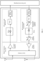
- FIG. 1 is a schematic diagram of a structure of a communication system according to an embodiment of this application.
- the communication system may be a terminal or a network equipment in embodiments of this application.
- the communication system may include a plurality of components, for example, a memory, a baseband processing unit, a radio frequency integrated circuit (radio frequency integrated circuit, RFIC), a radio frequency front end (radio frequency front end, RFFE) device, and an antenna (antenna, ANT). These components may be coupled by using various interconnection buses or other electrical connection manners.
- RFIC radio frequency integrated circuit
- RFFE radio frequency front end
- antenna antenna
- an antenna 1 represents a first antenna
- an antenna N represents an N th antenna
- N is a positive integer greater than 1.
- Different numbers indicate different paths.
- Each path may represent a signal processing channel.
- the receive path may include a feedback receive path (FBRx), a primary receive path (PRx), and a diversity receive path (DRx).
- the path may further be distinguished between a high frequency, a low frequency, and a baseband.
- the high frequency or the low frequency may be a relative high or low frequency.
- a communication system may include more or fewer paths, including more or fewer components.
- a radio frequency integrated circuit including an RFIC 1 and one or more optional RFICs 2 and a radio frequency front end device may jointly form a radio frequency sub-system.
- the radio frequency sub-system may be divided into an RF receive path (RF receive path) and an RF transmit path (RF transmit path).
- the RF transmit path may transmit a radio frequency signal through an antenna
- the RF receive path may receive the radio frequency signal through the antenna, and perform processing (for example, amplification, filtering, and down-conversion) on the radio frequency signal to obtain a baseband signal, and transmit the baseband signal to the baseband processing unit.
- the RF transmit path may receive a baseband signal from the baseband processing unit, perform processing (for example, up-conversion, amplification, and filtering) on the baseband signal to obtain a radio frequency signal, and finally radiate the radio frequency signal to space through the antenna.
- the radio frequency integrated circuit may be referred to as a radio frequency processing chip or a radio frequency chip.
- the radio frequency sub-system may include electronic devices such as an antenna switch, an antenna tuner, a low noise amplifier (low noise amplifier, LNA), a power amplifier, a mixer (mixer), a local oscillator (local oscillator, LO), and a filter (filter). These electronic devices may be integrated into one or more chips as required.
- the radio frequency integrated circuit may be referred to as a radio frequency processing chip or a radio frequency chip.
- the radio frequency front end device may also be an independent chip.
- the radio frequency chip is sometimes referred to as a receiver (receiver), a transmitter (transmitter), or a transceiver (transceiver).
- the antenna sometimes may also be considered as a part of the radio frequency sub-system, and may be integrated into a chip of the radio frequency sub-system.
- the antenna, the radio frequency front end device, and the radio frequency chip can all be manufactured and sold separately.
- the radio frequency sub-system may also use different devices or different integration manners based on power consumption and performance requirements. For example, some devices belonging to the radio frequency front end are integrated into a radio frequency chip, or even both the antenna and the radio frequency front end device are integrated into a radio frequency chip.
- the radio frequency chip may also be referred to as a radio frequency antenna module or an antenna module.
- the radio frequency signal is usually an analog signal
- a signal processed by the baseband processing unit is mainly a digital signal
- an analog to digital conversion component is further required in the communication system.
- the analog to digital conversion component may be disposed in the baseband processing unit, or may be disposed in the radio frequency sub-system.
- the analog to digital conversion component includes an analog to digital converter (analog to digital converter, ADC) that converts an analog signal into a digital signal, and a digital to analog converter (digital to analog converter, DAC) that converts a digital signal into an analog signal.
- ADC analog to digital converter
- DAC digital to analog converter
- the baseband processing unit may include one or more processors.
- the baseband processing unit may further include one or more hardware accelerators (hardware accelerators, HACs).
- the hardware accelerator may be configured to specially complete some sub-functions with relatively high processing overheads, for example, assembling and parsing a data packet (data packet), and encrypting and decrypting a data packet. These sub-functions may also be implemented by using a processor with a general function. However, in consideration of performance or costs, using the hardware accelerator may be more appropriate.
- the hardware accelerator is mainly implemented by using an application specific integrated circuit (application specified integrated circuit, ASIC).
- the hardware accelerator may also include one or more relatively simple processors, for example, an MCU.
- the baseband processing unit and the radio frequency sub-system jointly form a communication sub-system, to provide a wireless communication function for the communication system.
- the baseband processing unit is responsible for managing software and hardware resources of the communication sub-system, and may configure an operating parameter of the radio frequency sub-system.
- a processor of the baseband processing unit may run a sub-operating system of the communication sub-system.
- the sub-operating system may be an embedded operating system or a real time operating system (real time operating system).
- the baseband processing unit may be integrated into one or more chips, and the chip may be referred to as a baseband processing chip or a baseband chip.
- the baseband processing unit may be used as an independent chip, and the chip may be referred to as a modem (modem) or a modem chip.
- the baseband processing unit may be manufactured and sold in a unit of the modem chip.
- the modem chip is sometimes also referred to as a baseband processor or a mobile processor.
- the baseband processing unit may be further integrated into a larger chip, and manufactured and sold in a unit of the larger chip.
- the larger chip may be referred to as a system chip, a chip system, or a system on chip (system on a chip, SoC), or a SoC chip for short.
- Software components of the baseband processing unit may be built in hardware components of the chip before the chip is delivered, or may be imported from another non-volatile memory to hardware components of the chip after the chip is delivered, or may be downloaded and updated online through
- the communication system further includes a memory.
- the baseband processing unit may further include one or more caches.
- the memory may be classified into a volatile memory (volatile memory) and a non-volatile memory (non-volatile memory, NVM).
- the volatile memory is a memory in which data stored in the memory is lost when a power supply is interrupted.
- the volatile memory is mainly a random access memory (random access memory, RAM), including a static random access memory (static RAM, SRAM) and a dynamic random access memory (dynamic RAM, DRAM).
- RAM random access memory
- SRAM static random access memory
- DRAM dynamic random access memory
- the non-volatile memory is a memory in which data stored in the memory is not lost even if a power supply is interrupted.
- a common non-volatile memory includes a read only memory (read only memory, ROM), an optical disc, a magnetic disk, various memories based on a flash memory (flash memory) technology, and the like.
- the volatile memory may be used for the memory and the cache, and the non-volatile memory may be used for a mass memory, such as a flash memory.
- embodiments of this application are not limited to the communication system shown in FIG. 1 .
- a name of the device shown in FIG. 1 is merely used as an example for description herein, and is not intended to limit a device or a network element included in a communication system architecture to which this application is applicable.
- FIG. 2 is a schematic diagram of a structure of another communication system according to an embodiment of this application.
- FIG. 2 shows some common devices used for radio frequency signal processing in a communication system. It should be understood that although FIG. 2 shows only an RF receive path and an RF transmit path, the communication system in this embodiment of this application is not limited thereto.
- the communication system may include one or more RF receive paths and one or more RF transmit paths.
- Each RF transmit path may include devices such as a digital to analog converter (DAC) and a mixer.
- DAC digital to analog converter
- the RF receive path may include devices such as a mixer, a filter, and an analog to digital converter (ADC).
- ADC analog to digital converter
- An antenna that is received by the RF receive path from the antenna may be further processed by a device such as a low noise amplifier (low noise amplifier, LNA).
- a device such as a low noise amplifier (low noise amplifier, LNA).
- FIG. 2 is merely an example. Devices included in the RF receive path and the RF transmit path are not listed one by one in this embodiment of this application.
- to-be-transmitted information may be encoded, and a symbol may represent one or more binary bits of the information.
- Each symbol is encoded as a different combination of amplitude and phase modulation of a carrier.
- a higher modulation requires a higher resolution of encoded and modulated data, and correspondingly, a higher requirement on linearity of the power amplifier.
- power amplification may be performed through a digital PA (digital PA, DPA).
- DPA digital PA
- the DPA combines a high efficiency feature of a switching PA and uses a multi-bit quantization technology to convert the analog signal into the digital signal, and then amplifies a quantization level on each quantization bit in the digital signal, so as to obtain an amplified signal based on each amplified quantization level.
- a binary encoding mode of the digital signal may be converted into a thermometer encoding mode, and a quantization bit value on each quantization bit may be represented by an encoded value by performing the thermometer encoding. Therefore, the corresponding quantization level on each quantization bit may also be determined based on the encoded value by performing the thermometer encoding.
- a quantity of transistors that correspondingly amplify a quantization level on an i th quantization bit is 2 i -1, where i is an integer less than K.
- K is a quantity of quantization bits corresponding to a to-be-amplified signal.
- a quantity of transistors that correspondingly amplify the amplified quantization level is 2 9 -1. That is, each quantization level in the encoded digital signal is sent to a transistor that correspondingly amplifies the quantization level for power amplification, so as to ensure a linearity requirement of the DPA amplified signal and improve efficiency of the power amplifier.
- a DPA receives an analog signal of a baseband processing unit.
- the analog signal may be quantized into a digital signal through a DAC module.
- a binary code may be converted into a thermometer code.
- the digital signal passes through a corresponding filter, for example, an up-sampling interpolation filter, to convert a low-frequency signal of baseband data into a high-frequency signal having a radio frequency carrier, so as to improve an out-of-band signal-to-noise ratio of the signal, thereby meeting a requirement of a spectrum of a protocol.
- a coordinate rotation digital computer (coordinate rotation digital computer, CORDIC) unit divides the digital signal into an amplitude signal and a phase signal.
- the amplitude signal is input to the DPA.
- the phase signal is converted into a radio frequency signal (also a phase-modulated (phase-modulated, PM) signal) by the modulator and input to the DPA.
- the DPA combines the input amplitude signal and the input phase-modulated signal, amplifies the signal, and outputs the amplified signal to the antenna.
- an input signal includes an in-phase input signal I and a quadrature input signal Q, and the signal I and the signal Q in the input signal have a 90-degree phase difference.
- the signal I and the signal Q are input into a digital to analog converter (DAC) 1 and a digital to analog converter (DAC) 2, and the digital to analog converter 1 performs digital to analog conversion on the signal I and outputs the signal I to a filter 1.
- the filter 1 may be a low-pass filter, and the filter 1 is configured to filter out a high frequency in a signal output by the digital to analog converter 1. After performing digital to analog conversion on the signal Q of the digital to analog converter 2, the digital to analog converter 2 outputs the signal Q to the filter 2.
- the filter 2 may be a low-pass filter, and the filter 2 is configured to filter out a high frequency in a signal output by the digital to analog converter 2.
- a mixer performs frequency mixing on the signals output by the filter 1 and the filter 2, and outputs a radio frequency carrier. Amplitude modulation (that is, power amplification) of the radio frequency carrier is implemented through the DPA.
- the two signals namely, the signal I and the signal Q, are input to a quantized DPA for combination, and are finally output to the antenna.
- the following uses decoding and amplification of an amplitude signal in the polar architecture in FIG. 3 as an example for description.
- For an amplification process of the signal I and the signal Q in the IQ architecture refer to a process of decoding and driving amplification of the amplitude signal in the example in FIG. 4 .
- the DPA may include a decoder and a transistor array.
- the decoder is configured to receive a digital signal sent by the baseband processing unit.
- a transistor in the transistor array may be a switched-capacitor power amplifier (switched-capacitor power amplifier, SCPA).
- SCPA switched-capacitor power amplifier
- the amplitude signal in the digital signal is transferred to the decoder of the DPA.
- the amplitude signal may include quantization bit values corresponding to K quantization bits, and the quantization bit value may be represented as an amplitude control word (amplitude control word, ACW).
- the decoder is configured to decode the amplitude control word in the amplitude signal, determine a corresponding quantization level of each quantization bit in the digital signal, and determine a corresponding transistor in the DPA that is driven by each quantization level.
- the ACW is binary encoded. For example, it is determined that the ACW is 4 bits, that is, a quantity of quantization bits of the DPA is 4. Each bit corresponds to a transistor that controls a DPA. In this case, the transistor array in the DPA includes four transistors.
- the decoder may determine, through the ACW, a switch status of a transistor corresponding to each bit.
- the ACW is 1010
- a 0 th bit is 0, a corresponding transistor is in a non-operating state
- a first bit is 1
- a corresponding transistor is configured to amplify a quantization level corresponding to the first bit
- a second bit is 0, a corresponding transistor is in the non-operating state
- a third bit is 1
- a corresponding transistor is configured to amplify a quantization level corresponding to the third bit.
- the decoder decodes the received digital signal, and generates a corresponding quantization level after determining the transistor in a driven DPA.
- a digital gate With reference to a phase-modulated signal, a digital gate combines the phase-modulated signal with the quantization level from the decoder, to generate square wave vectors of the quantization level. After the square wave vectors are fed into a transistor that amplifies the quantization level, the quantization level is amplified. All the amplified quantization levels are transferred to an impedance matching network, and the impedance matching network is configured to adjust load impedance of the DPA.
- the DPA has relatively poor linearity for a binary-encoded digital signal, when a requirement for quantization precision of the digital to analog conversion is relatively high, for example, a quantity of quantization bits of the DPA is 15 bits, in this case, a transistor that is driven by the binary code cannot be directly used to implement power amplification.
- each encoded bit is implemented by a transistor controlled by the thermometer code, that is, each time a quantization bit is added, a quantity of transistors added in the DPA increases exponentially.
- a quantity of quantization bits is K
- a quantity of transistors required for amplifying a quantization level corresponding to an i th quantization bit is 2 i , where i is an integer less than K.
- the quantity of transistors in the DPA reached 2 K -1.
- the quantization bits of the ACW are 15 bits, that is, the quantity of quantization bits of the DPA is 15, and each quantization bit is implemented by a transistor controlled by thermometer encoding
- the quantity of transistors in the DPA reaches 2 15 -1.
- a quantization level corresponding to a 0 th bit is amplified through one transistor
- a first bit is correspondingly amplified through three transistors
- a second bit is correspondingly amplified through three transistors
- a third bit is correspondingly amplified through seven transistors
- ... and a seventeenth bit is correspondingly controlled by 2 14 -1 transistors.
- the encoding may be performed in a manner of hybrid encoding of a thermometer code and a binary code, and take 15 bits are used as an example.
- the high-order 10 bits are implemented by a transistor that uses the thermometer code
- the low-order 5 bits are implemented by a transistor that uses the binary code.
- the decoder decodes each bit in the 10 bits according to a high-order thermometer encoding manner, so as to correspondingly control the transistor of each bit in the 10 bits, and decodes each bit in the 5 bits according to a low-order binary encoding manner, so as to correspondingly control the transistor of each bit in the 5 bits.
- the DPA includes (1023 + 5) transistors.
- a layout requirement needs to be considered for the DPA. For example, a transistor array of 32 rows ⁇ 32 columns is arranged, which increases difficulty in layout design of a decoder and a transistor array of the DPA in an entire circuit.
- the quantity of transistors increases exponentially with the quantity of quantization bits of transistors in the DPA.
- the quantization precision of the DPA is related to the quantity of transistors, and the two are exponentially related. If the precision needs to be further improved, for example, the DPA precision of 16 bits, the quantity of transistors may reach (2047+5).
- the design difficulty of a layout is greatly increased, and a more complex decoder needs to be designed, which additionally increases the power consumption of the digital amplifier.
- the digital power amplifier includes a decoder and N transistor sets.
- the decoder includes an input end and N groups of output ends, the input end of the decoder is connected to a baseband processing unit, the N groups of output ends of the decoder are respectively connected to the N transistor sets, and the N transistor sets operate within at least two different operating voltage ranges.
- the decoder is configured to receive K quantization levels corresponding to a to-be-amplified signal from the baseband processing unit, and send a target quantization level that is within a same operating voltage range and that is of the K quantization levels to a transistor set that operates within the operating voltage range, where N is a positive integer greater than 1, and K is a positive integer.
- the N transistor sets are configured to respectively amplify target quantization levels received by the N transistor sets.
- At least two different operating voltage ranges of the N transistor sets may be determined by a voltage range of the to-be-amplified signal.
- the to-be-amplified signal may determine a corresponding voltage range based on a modulation scheme.
- FIG. 7a is a time envelope signal of an "OFDM+quadrature amplitude modulation (quadrature amplitude modulation, QAM) signal. It may be determined, based on the time envelope signal, that the voltage range of the to-be-amplified signal is [U1, U2]. U1 is less than U2, and U1 and U2 are rational numbers. Therefore, division is performed based on the voltage range of the to-be-amplified signal, to obtain at least two voltage ranges. For example, a voltage range 1 is included, that is, [U1, U0], and a voltage range 2 is included, that is, [U0, U2]. U0 is less than U2 and greater than U1. U0 is a rational number.
- operating voltage ranges corresponding to the N transistor sets include at least the voltage range 1 or the voltage range 2.
- an operating voltage range 1 of at least one transistor set in the N transistor sets includes at least the voltage range 1, for example, [U1, U0'], where U0' is greater than or equal to U0, U0 is less than U2 and greater than U1, and U0' is a rational number.
- the at least one transistor set is configured to amplify a quantization level within the operating voltage range 1.
- each of the N transistor sets corresponds to one or more of K quantization bits. Therefore, the decoder may determine, based on the one or more of the K quantization bits corresponding to each of the N transistor sets, a target quantization bit of the target quantization level in the K quantization bits, and send the target quantization level to a transistor set corresponding to the target quantization bit.
- each of the N transistor sets may be specifically corresponding to one or more of the K quantization bits in a plurality of manners.
- the following uses manner 1 to manner 2 as an example for description.
- Manner 1 At least two transistor sets in the N transistor sets operate within a first operating voltage range, the first operating voltage range includes at least two voltage sub-ranges in which voltage values do not overlap, and the at least two voltage sub-ranges are in a one-to-one correspondence with the at least two transistor sets.
- the decoder is configured to send a target quantization level that is within a same voltage sub-range and that is of the K quantization levels to a transistor set corresponding to the voltage sub-range.
- the transistor set corresponding to the voltage sub-range is configured to amplify a received quantization level within the voltage sub-range.
- the first operating voltage range is a range of the to-be-amplified signal, that is, [U1, U2].
- the first operating voltage range includes at least two voltage sub-ranges in which voltage values do not overlap: a voltage sub-range 1, [U1, V1], and a voltage sub-range 2, [V1, U2].
- Each voltage sub-range may correspond to a quantity of quantization bits within the voltage sub-range, so that the quantity of quantization bits of the first operating voltage range is determined based on a sum of the quantities of quantization bits within the voltage sub-ranges.
- the quantity of transistors in the transistor set may be determined based on the quantity (K) of quantization bits of the DPA and the quantity of quantization bits that are set within each voltage sub-range and that are corresponding to the voltage sub-range.
- a quantity of quantization bits corresponding to each voltage range or voltage sub-range may be implemented in a plurality of manners.
- the following uses a voltage range as an example, and uses a manner A to a manner C as an example for description.
- the quantity of quantization bits of each voltage sub-range is the same. That is, when the quantity of quantization bits corresponding to the first operating voltage range is 12, the quantity of quantization bits of each voltage sub-range may be 6.
- the quantization bit of the transistor set is related to the operating voltage range corresponding to the transistor set.
- the voltage sub-range 1 corresponds to a DPA quantization bit that is a low-order quantization bit
- the voltage sub-range 2 corresponds to a DPA quantization bit that is a high-order quantization bit.
- the voltage sub-range 1 corresponds to six low-order quantization bits of the DPA quantization bits
- the voltage sub-range 2 corresponds to six high-order quantization bits of the DPA quantization bits.
- the voltage sub-range 1 corresponds to a transistor that is of the transistor set and that is configured to amplify a quantization level in the voltage sub-range 1
- the voltage sub-range 2 corresponds to a transistor that is of the transistor set and that is configured to amplify a quantization level in the voltage sub-range 2. Therefore, a maximum quantity of transistors required for the first operating voltage range is 2 6 -1. In this case, a quantity of transistors that amplify the first operating voltage range in the DPA is 127.
- a low-bit transistor set corresponding to the voltage sub-range 1 may further be combined with a binary encoding manner, for example, including three binary-encoded bits and three thermometer-encoded bits.
- a quantity of transistors in the transistor set corresponding to a first voltage range is 2 3 +3.
- a voltage range of an envelope amplitude of the time envelope signal shown in FIG. 7a is divided into six voltage ranges.
- one voltage range corresponds to one operating voltage range of one transistor set
- six operating voltage ranges of the six transistor sets may be correspondingly determined.
- FIG. 7b an example in which quantities of quantization bits corresponding to all operating voltage ranges are the same is still used.
- the quantity of quantization bits of the DPA is 12, the quantity of quantization bits of each operating voltage range may be 2. Therefore, a maximum quantity of transistors required for each voltage range is 2 2 -1. In this case, the quantity of transistors in the DPA is 24.
- N may be correspondingly set, so as to meet requirements of DPA precision, layout design, and cost control.
- the N transistor sets operate within different consecutive N voltage ranges, different power supplies are used to supply power to corresponding transistor sets within different voltage ranges.
- the voltage range of the analog signal amplified by the DPA is obtained by combining the N voltage ranges.
- Power amplifiers of corresponding transistor sets are driven through different voltage ranges, so as to perform power amplification on IQ signals of different amplitudes.
- a magnitude of an envelope amplitude of the time envelope signal is divided into six consecutive voltage ranges, including [0, 0.6] V, [0.6, 1.2] V, ..., [3, 3.6] V. Therefore, six transistor sets may be set, and an operating voltage range of each transistor set includes at least one voltage range, to amplify the quantization level within the voltage range.
- each voltage range corresponds to two quantization bits.
- a quantization bit value corresponding to the signal may be 0000000011111, that is, two lowest bits correspondingly drive transistors in the transistor set corresponding to the first voltage range, and are configured to amplify two quantization levels on the two lowest bits.
- the two consecutive bits correspondingly drive transistors corresponding to the second voltage range, and are configured to amplify two quantization levels on the two bits corresponding to the voltage range.
- the fifth bit correspondingly drives some transistors within the third voltage range, which are configured to amplify a quantization level on the fifth bit corresponding to the voltage range. In this way, quantization levels on the five quantization bits are amplified.
- a magnitude of a voltage range is determined based on a probability that a voltage value of an envelope signal of an analog signal of the to-be-amplified signal appears within the operating voltage range.
- a quantity of quantization bits corresponding to a voltage range is determined based on a probability that a voltage value of an envelope signal of an analog signal of the to-be-amplified signal appears within the operating voltage range.
- any operating voltage range in the N operating voltage ranges, a magnitude of the operating voltage range or a quantity of quantization bits corresponding to a transistor set that operates within the operating voltage range is related to a probability that a voltage value of an envelope signal of an analog signal of the to-be-amplified signal appears within the operating voltage range.
- an amplitude of the time envelope signal changes significantly, and a larger amplitude of the envelope signal indicates a lower probability, and a smaller amplitude of the envelope signal indicates a higher probability of occurrence of an amplitude value of the envelope signal.
- N voltage ranges may be divided based on the probability of occurrence of the amplitude of the envelope signal. A voltage range with a higher probability is smaller, and a voltage range with a lower probability is larger, so as to ensure a linearity requirement of signal transmission.
- a magnitude of the voltage range is determined based on a probability that the voltage range corresponds to power spectral density of an envelope signal of the to-be-amplified signal.
- a quantity of quantization bits corresponding to the voltage range is determined based on a probability that the voltage range corresponds to power spectral density of an envelope signal of the to-be-amplified signal.
- a magnitude of the operating voltage range or a quantity of quantization bits of a transistor set that operates within the operating voltage range is related to a probability that power spectral density of an envelope signal of an analog signal of the to-be-amplified signal appears within the operating voltage range.
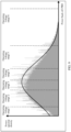
- a horizontal axis in FIG. 9 is a normalized value obtained by taking a logarithm of an amplitude value of an envelope signal of an analog signal of a to-be-amplified signal, and may correspond to a power back-off amount of a transistor.
- a vertical axis is power spectral density corresponding to different amplitude values, that is, may correspond to a probability that a transistor amplifies a quantization level in different voltage ranges.
- a region with higher power spectral density has a higher frequency of the transistor that operates within the voltage range, and efficiency may be reduced after power back-off, a region with a higher power spectral density probability may be divided into a smaller voltage range, so as to reduce a power back-off value of the transistor that amplifies the quantization level within the voltage range, and ensure the linearity requirement of signal transmission.
- the quantity of quantization bits of the DPA is a sum of quantities of quantization bits of the quantization levels that are correspondingly amplified by the N transistor sets and that are of the N voltage ranges. Therefore, after the quantization bits of the quantization levels that are correspondingly amplified by the N transistor sets and that are of the N voltage ranges and the quantization levels are determined, the quantity of transistors in the transistor sets that amplify the quantization levels within the voltage range may be correspondingly determined.
- the following uses a manner B 1 and a manner B2 as examples for description.
- a quantity of quantization bits corresponding to a voltage range is related to a magnitude of the voltage range. For example, when the voltage range is relatively large, a relatively large quantity of quantization bits may be set. With reference to FIG. 9 , when a first voltage range is relatively large, a relatively large quantity of quantization bits may be set, for example, three bits, and when a third voltage range is relatively small, a relatively small quantity of quantization bits may be set, for example, two bits.
- a quantity of quantization bits corresponding to the voltage range may be determined based on a probability that a voltage range of an envelope signal of an analog signal of the to-be-amplified signal appears within the voltage range.
- a relatively large quantity of quantization bits may be set within the voltage range of the envelope signal of the analog signal.
- a relatively small quantity of quantization bits for example, two bits
- a relatively large quantity of quantization bits for example, three bits
- a relatively large quantity of quantization bits for example, four bits
- a relatively small quantity of quantization bits for example, one bit, may be set.
- the bits may sequentially correspond to 2.6 bits, 3 bits, 4 bits, 3 bits, 3 bits, 2 bits, and 1 bit.
- quantization bits respectively corresponding to the N transistor sets form quantization bits of the DPA.
- a voltage range of quantization levels correspondingly amplified by each transistor set may be determined based on the power spectral density in FIG. 9 .
- a quantity of quantization bits corresponding to each voltage range may also be determined based on the power spectral density in FIG. 9 .
- the quantity of quantization bits of the voltage range is determined based on the magnitude of the voltage range.
- the quantity of quantization bits of the voltage range is determined based on the probability of the power spectral density corresponding to the voltage range in the power spectral density of the envelope signal of the analog signal of the to-be-amplified signal. For a specific manner, refer to the manner B1 and the manner B2. Details are not described herein again.
- N voltage ranges of quantization levels correspondingly amplified by N transistor sets may be discontinuous. For example, at least two voltage ranges may overlap.
- the overlap herein may be partial overlap, or may be full overlap.
- two transistor sets in the N transistor sets correspond to a same operating voltage range, and the two transistor sets correspond to different quantities of quantization bits.
- the decoder may be further configured to: determine, from the K quantization levels, a target quantization level within the operating voltage range corresponding to the two transistor sets; select, from the two transistor sets, a target transistor set whose quantity of quantization bits is the same as a quantity of quantization bits corresponding to the target quantization level; and send the target quantization level corresponding to the operating voltage range to the target transistor set.
- the N transistor sets include a transistor set 3-1 and a transistor set 3-2, an operating voltage range corresponding to the transistor set 3-1 includes a voltage range 3, an operating voltage range corresponding to the transistor set 3-2 includes a voltage range 3, and the voltage range 3 is less than a voltage range corresponding to the to-be-amplified signal.
- a quantity of quantization bits corresponding to the transistor set 3-1 is K1
- a quantity of quantization bits corresponding to the transistor set 3-2 is K2, where K1 and K2 are positive integers less than K.
- K is a different value, that is, when quantization precision of the to-be-amplified signal is different, a quantity of quantization bits of a quantization level within an input voltage range 3 may change.
- a target transistor set whose quantity is the same as the quantity of quantization bits corresponding to the target quantization level may be selected based on the quantity of quantization bits corresponding to the transistor set 3-1 and the quantity of quantization bits corresponding to the transistor set 3-2. For example, when the quantity of quantization bits corresponding to the target quantization level within the voltage range 3 is K1, in this case, it may be determined that the target transistor set is the transistor set 3-1. Therefore, the decoder inputs K1 quantization levels within the voltage range 3 to the transistor set 3-1, to implement amplification of the K1 quantization levels.
- a transistor set that matches quantization precision in a corresponding voltage range is selected, thereby improving flexibility and an application range of the DPA amplified signal.
- the following uses a voltage range corresponding to the to-be-amplified signal as an example for description. By setting operating voltage ranges corresponding to different transistor sets and voltage ranges of quantization levels correspondingly amplified by different transistor sets, quantization precision of the to-be-amplified signal is adjusted.
- the following uses a manner 2-1 and a manner 2-2 as examples.
- Manner 2-1 As shown in FIG. 10b , the voltage range of the envelope amplitude of the time envelope signal shown in FIG. 7a is divided into four voltage ranges, which are [U1, V2], [V2, V1], [V1, V3] and [V3, U2].
- an operating voltage range of a first transistor set corresponds to [U1, V1]
- an operating voltage range of a second transistor set corresponds to [V2, V3]
- an operating voltage range of a third transistor set corresponds to [V3, U2].
- V1 is greater than V2
- V3 is greater than V4.
- a quantity of quantization bits of the first transistor set is 7, a quantity of quantization bits of the second transistor set is 8, and a quantity of quantization bits of the third transistor set is 5.
- the decoder may determine, based on the quantity of quantization bits corresponding to each voltage range and the quantity of quantization bits corresponding to each transistor set, a quantization level correspondingly amplified by each transistor set within the voltage range.
- the quantity of quantization bits of the DPA is 12, and the quantities of quantization bits of each voltage range corresponding to ascending order are 3, 4, 4, and 2, seven quantization levels within the voltage ranges [U1, V2] and [V2, V1] may be amplified through the first transistor set. Six quantization levels within the voltage range [V1, V3], [V3, U2] are amplified through the third transistor set.
- the quantity of quantization bits of the DPA is 10
- the quantities of quantization bits of the voltage ranges corresponding to the ascending order are 2, 4, 4, and 1
- two quantization levels within the voltage range [U1, V2] may be amplified through the first transistor set
- eight quantization levels within the voltage ranges [V2, V1] and [V1, V3] may be amplified through the second transistor set.
- One quantization level within the voltage range [V4, U2] is amplified through the third transistor set.
- Manner 2-2 Voltage ranges of quantization levels correspondingly amplified by the N transistor sets partially overlap.
- the voltage range of the envelope amplitude of the time envelope signal shown in FIG. 7a is divided into five voltage ranges, for example, [U1, V2], [V2, V1], [V1, V4], [V4, V3] and [V3, U2] in ascending order.
- operating voltage ranges of three transistor sets are [U1, V1], [V2, V3], and [V1, U2]
- amplified voltage ranges of the three transistor sets are also [U1, V1], [V2, V3], and [V1, U2].
- V1 is greater than V2
- U2 is greater than V1.
- a first non-overlapping voltage range corresponds to [U1, V2]
- a second non-overlapping voltage range corresponds to [V2, V4]
- a third non-overlapping voltage range corresponds to [V4, U2].
- Two overlapping voltage ranges are determined: a first overlapping voltage range corresponds to [V2, V1], and a second overlapping voltage range corresponds to [V4, V3].
- a target transistor set corresponding to the quantization bit may be correspondingly selected.
- the decoder may sequentially determine that the quantity of quantization bits corresponding to the voltage range is 2.
- the decoder may sequentially determine that the quantity of quantization bits corresponding to the voltage range is 2.
- four quantization levels within the first to second voltage ranges may be amplified through the first transistor set
- quantization levels of two quantization bits within the third voltage range may be amplified through the second transistor set
- four quantization levels within the fourth to fifth voltage ranges may be amplified through the third transistor set.
- the amplified quantization level of each transistor set may be further determined in another manner, provided that the transistor set is capable of amplifying the quantization level.
- different operating voltage ranges may be selected based on different signals to amplify the signal.
- different operating voltage ranges may be selected based on different quantization precision requirements to amplify the signal. Therefore, requirements of quantization precision of different signals may be more flexibly adapted, and flexibility of the DPA is improved without redesigning the layout of the DPA.
- the operating voltages of the transistor sets may be different.
- structures of transistors in different transistor sets may also be different.
- a higher operating voltage indicates a larger quantity of transistors that need to be stacked.
- the transistor in this application may be a MOS transistor, or may be another transistor of a switching PA. This is not limited herein.
- three types of transistors shown in FIG. 11 are implemented based on the process, and maximum values of operating voltages of the three types of transistors are 1.2 V, 2.4 V, and 3.6 V.
- a transistor 1 may be used in a transistor set corresponding to a voltage range below 1.2 V
- a transistor 2 may be used in a transistor set corresponding to a voltage range below 2.4 V
- a transistor 3 may be used in a transistor set corresponding to a voltage range below 2.4 V.
- the transistor 2 and the transistor 3 include superposition of a plurality of transistors, there may be a plurality of power supply ports.
- the transistor 2 includes power supply ports of two operating voltages
- the transistor 3 includes power supply ports of three operating voltages.
- a specific power supply voltage may be set according to an actual requirement, and is not limited herein.
- the transistor set includes at least one transistor, and the at least one transistor uses a same operating voltage. Therefore, a circuit design solution may be simplified, and layout design costs and process difficulty may be reduced.
- the transistor set may further include a first switched capacitor, and the first switched capacitor is connected to all transistors in the transistor set.
- the first switched capacitor is configured to receive a quantization level corresponding to the transistor set, and transmit the quantization level to a connected transistor.
- the transistor is configured to amplify the quantization level sent by the switched capacitor.
- the transistor set may further include: each second switched capacitor connected to each transistor in the transistor set.
- Each second switched capacitor is configured to receive a quantization level corresponding to the transistor set, and transmit the quantization level to a connected transistor.
- the transistor is configured to amplify the quantization level sent by the switched capacitor.
- operating voltages of all transistors in the transistor set may be different operating voltages, or may be a same operating voltage.
- Transistors in each transistor set operate at different operating voltages.
- the transistor in the transistor set uses a switched capacitor architecture, and each switched capacitor is controlled to be turned on or off by using a quantization level correspondingly amplified by each transistor.
- the DPA may include an impedance matching network, and the impedance matching network may be configured to match impedance of the N transistor sets.
- the impedance matching network may be configured to match impedance of the N transistor sets.
- a resistor shown in FIG. 13 may be configured to match impedance of the N transistor sets.
- the DPA may further include an inductor.
- the inductor is configured to implement resonance with a capacitor (for example, a first switched capacitor or a second switched capacitor) in the DPA, and control an operating frequency of the DPA.
- operating voltages of all transistors in the transistor set are a same operating voltage.
- Voutn is an output voltage of an n th transistor set
- Vn is an operating voltage of each transistor set
- Cn is a total capacitance of each transistor set
- Ratio n is a ratio of switches in each transistor set being turned on
- Poutn is an output power of the n th transistor set.
- the DPA may be further combined with a method such as a load modulation technology and a power supply modulation technology, to further improve efficiency of the power amplifier, thereby reducing power consumption of the DPA.
- FIG. 15 is an example of a schematic diagram of a structure of a Doherty power amplifier.
- the Doherty power amplifier includes a first power amplification unit, a second power amplification unit, and an impedance transformation network.
- the first power amplification unit is a primary power amplifier
- the second power amplification unit is a secondary power amplifier
- the first power amplification unit is a secondary power amplifier
- the second power amplification unit is a primary power amplifier.
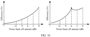
- an operating region of the Doherty power amplifier may be roughly divided into three stages: a low-power region, a backoff return, and a full-power region. The following describes the three phases in detail with reference to an efficiency curve chart of the Doherty power amplifier in FIG. 16 .
- a bias mode of the circuit (peak circuit) of the secondary power amplifier is class C, and input power of the secondary power amplifier is insufficient to drive the secondary power amplifier to work.
- the peak path is open-circuited.
- the impedance of the circuit (main circuit) of the primary power amplifier remains unchanged.
- the primary power amplifier enters a saturation state, and the voltage reaches a full swing, to implement a first high power point during operation of the Doherty power amplifier. For example, as shown in FIG.
- a power back-off point corresponding to the first high power point of the power amplifier is 6 dB, that is, the input power of the power amplifier is 6 dB less than that when both the primary power amplifier and the secondary power amplifier in the power amplifier have full power.
- a peak circuit As the input power of the power amplifier gradually increases, a peak circuit is opened. In this case, the impedance of a main circuit gradually decreases, but the voltage of the main circuit is always full swing and remains in a saturation state. At the same time, the impedance of the peak circuit also gradually decreases, and the voltage gradually increases, but does not reach the saturation state. Therefore, operating efficiency of the Doherty power amplifier slightly decreases.
- both the main circuit and the peak circuit reach the saturation state, and both the voltages reach a full swing.
- the Doherty power amplifier implements a second high power point during operation. For example, as shown in FIG. 16 , a power back-off point of the power amplifier corresponding to a second high-power point is 0 dB. In this case, the power amplifier is in a maximum output power state in the entire system.
- the digital power amplifier in this application may further improve efficiency of the DPA power amplifier with reference to a Doherty principle.
- the DPA in this embodiment of this application may include a first power amplification unit, a second power amplification unit, and a combination unit.
- the N transistor sets are located in the first power amplification unit and/or the second power amplification unit.
- the first power amplification unit is configured to amplify a first sub-signal of the to-be-amplified signal to obtain a first amplified sub-signal, and send the first amplified sub-signal to the combination unit.
- the second power amplification unit is configured to amplify a second sub-signal of the to-be-amplified signal to obtain a second amplified sub-signal, and send the second amplified sub-signal to the combination unit.
- the combination unit is configured to combine the first amplified sub-signal and the second amplified sub-signal to obtain a target amplified signal corresponding to the to-be-amplified signal.
- a signal from the baseband processing unit may be divided into a first sub-signal and a second sub-signal, and the first sub-signal and the second sub-signal are divided into two channels, and are input to the first power amplification unit and the second power amplification unit. Therefore, the first sub-signal may be amplified by the first power amplification unit, and the second sub-signal may be amplified by the second power amplification unit.
- the first amplified sub-signal amplified by the first power amplification unit and the second amplified sub-signal amplified by the second power amplification unit may be combined through the combination unit, so as to obtain the target amplified signal corresponding to the to-be-amplified signal.
- the first power amplification unit and/or the second power amplification unit are/is combined with a power amplification manner of the N transistor sets in the DPA in this application, so that a quantity of transistors required in the first power amplification unit and/or the second power amplification unit may be reduced, and power amplification efficiency and a power amplification effect may be improved.
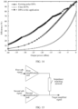
- FIG. 17 is a schematic diagram of a structure of a radio frequency power amplification system with an outphasing architecture.
- a signal control system (Signal Control System, SCS) splits an input baseband digital signal into two digital signals for output.
- SCS Signal Control System
- the digital to analog converter converts the digital signal into the analog signal
- an analog quadrature modulation (Analog Quadrature Modulation, AQM) module performs quadrature modulation on the analog signal, to output the radio frequency signal to the first power amplification unit and the second power amplification unit for power amplification.
- the two radio frequency signals are combined at the combiner.
- For a specific setting manner of the first power amplification unit and the second power amplification unit reference may be made to the setting manner of the first power amplification unit and the second power amplification unit in FIG. 17 , and details are not described herein again.
- another load modulation technology and power supply modulation technology may be further combined, for example, load modulation based on a transformer-based power synthesis network, or power supply modulation based on a Class-G dual power supply, to improve efficiency of a deep backoff region.
- connection in this application describes a connection relationship between two objects, and may represent two connection relationships.
- a connection between A and B may represent two cases: A is directly connected to B, and A is connected to B through C.
- terms “first” and “second” are only used to distinguish the purpose of the description, but cannot be understood as indication or implication of relative importance, and cannot be understood as an indication or implication of a sequence.
- the system structure and the service scenario provided in embodiments of this application are mainly intended to explain some possible implementations of the technical solutions of this application, and should not be construed as a unique limitation on the technical solutions of this application.
- a person of ordinary skill in the art may know that, with evolution of a system and emergence of an updated service scenario, the technical solutions provided in this application are also applicable to a same or similar technical problem.
Landscapes
- Engineering & Computer Science (AREA)
- Power Engineering (AREA)
- Microelectronics & Electronic Packaging (AREA)
- Computer Networks & Wireless Communication (AREA)
- Signal Processing (AREA)
- Amplifiers (AREA)
Applications Claiming Priority (2)
| Application Number | Priority Date | Filing Date | Title |
|---|---|---|---|
| CN202110389641.0A CN115208324A (zh) | 2021-04-12 | 2021-04-12 | 一种数字功率放大器及通信系统 |
| PCT/CN2021/135499 WO2022217945A1 (fr) | 2021-04-12 | 2021-12-03 | Amplificateur de puissance numérique et système de communication |
Publications (2)
| Publication Number | Publication Date |
|---|---|
| EP4311106A1 true EP4311106A1 (fr) | 2024-01-24 |
| EP4311106A4 EP4311106A4 (fr) | 2024-09-11 |
Family
ID=83570926
Family Applications (1)
| Application Number | Title | Priority Date | Filing Date |
|---|---|---|---|
| EP21936811.5A Pending EP4311106A4 (fr) | 2021-04-12 | 2021-12-03 | Amplificateur de puissance numérique et système de communication |
Country Status (3)
| Country | Link |
|---|---|
| EP (1) | EP4311106A4 (fr) |
| CN (1) | CN115208324A (fr) |
| WO (1) | WO2022217945A1 (fr) |
Family Cites Families (5)
| Publication number | Priority date | Publication date | Assignee | Title |
|---|---|---|---|---|
| US20100188148A1 (en) * | 2009-01-26 | 2010-07-29 | Texas Instruments Incorporated | Predistortion mechanism for compensation of transistor size mismatch in a digital power amplifier |
| CN203406835U (zh) * | 2013-09-02 | 2014-01-22 | 武汉芯泰科技有限公司 | 一种功率放大装置 |
| CN106797199B (zh) * | 2014-10-15 | 2020-11-27 | 华为技术有限公司 | 数字正交调制器和开关电容阵列电路 |
| US11424725B2 (en) * | 2018-08-01 | 2022-08-23 | Argo Semiconductors Fs Ltd (He 359654) | Digital power amplifier with filtered output |
| CN111865236B (zh) * | 2019-04-25 | 2022-07-26 | 华为技术有限公司 | 信号处理方法、装置及系统 |
-
2021
- 2021-04-12 CN CN202110389641.0A patent/CN115208324A/zh active Pending
- 2021-12-03 EP EP21936811.5A patent/EP4311106A4/fr active Pending
- 2021-12-03 WO PCT/CN2021/135499 patent/WO2022217945A1/fr not_active Ceased
Also Published As
| Publication number | Publication date |
|---|---|
| WO2022217945A1 (fr) | 2022-10-20 |
| CN115208324A (zh) | 2022-10-18 |
| EP4311106A4 (fr) | 2024-09-11 |
Similar Documents
| Publication | Publication Date | Title |
|---|---|---|
| CN106027132B (zh) | 在高峰均功率比信号下进行功率效率改进的相控阵列加权 | |
| EP2541781B1 (fr) | Architecture de transmetteur RF et procédé associé | |
| US10516424B2 (en) | Signal processing arrangement for a transmitter | |
| US20250392343A1 (en) | DIGITAL PRE-PROCESSING CHIP FOR mmWAVE TRANSCEIVER ARCHITECTURES | |
| CN106877828B (zh) | 变压器正交合成功率放大器 | |
| CN113196669A (zh) | 具有改善的效率和输出功率的rfdac(rf(射频)dac(数字到模拟转换器)) | |
| US10979276B2 (en) | Transmission method, transmission device, reception method, and reception device | |
| US20250192810A1 (en) | Signal processing system, remote radio unit, and antenna unit | |
| EP4131776A1 (fr) | Dispositif de communication sans fil, système, et procédé de traitement de signal | |
| CN112953576A (zh) | 信号发射机 | |
| CN113630094A (zh) | 基于多相位的多合体功率放大器方法及装置 | |
| CN114128138B (zh) | 一种信号处理方法及装置 | |
| Luo et al. | Empowering multifunction: Digital power amplifiers, the last RF frontier of the analog and digital kingdoms | |
| US10142050B2 (en) | Encoding modulation method and transmitter | |
| US11616478B2 (en) | Uplink multiple input-multiple output (MIMO) transmitter apparatus | |
| CN118056362B (zh) | 一种通信装置、通信方法及相关设备 | |
| CN115176426B (zh) | 一种射频电路、信号反馈电路和通信系统 | |
| WO2022217945A1 (fr) | Amplificateur de puissance numérique et système de communication | |
| CN103888155B (zh) | 射频发射机、集成电路器件、无线通信单元及相关方法 | |
| US20260088777A1 (en) | Digital power amplifier with analog clipping scheme | |
| EP4535657A1 (fr) | Dispositif d'amplification de puissance, unité radio distante, station de base et système de communication | |
| Chen et al. | A reconfigurable compact rf module for 5g | |
| Wang et al. | A Compact Quadrature Doherty Digital Power Amplifier with Backoff Efficiency Enhancement | |
| CN108352814A (zh) | 正交数字功率放大器 |
Legal Events
| Date | Code | Title | Description |
|---|---|---|---|
| STAA | Information on the status of an ep patent application or granted ep patent |
Free format text: STATUS: THE INTERNATIONAL PUBLICATION HAS BEEN MADE |
|
| PUAI | Public reference made under article 153(3) epc to a published international application that has entered the european phase |
Free format text: ORIGINAL CODE: 0009012 |
|
| STAA | Information on the status of an ep patent application or granted ep patent |
Free format text: STATUS: REQUEST FOR EXAMINATION WAS MADE |
|
| 17P | Request for examination filed |
Effective date: 20231019 |
|
| AK | Designated contracting states |
Kind code of ref document: A1 Designated state(s): AL AT BE BG CH CY CZ DE DK EE ES FI FR GB GR HR HU IE IS IT LI LT LU LV MC MK MT NL NO PL PT RO RS SE SI SK SM TR |
|
| RAP3 | Party data changed (applicant data changed or rights of an application transferred) |
Owner name: HUAWEI TECHNOLOGIES CO., LTD. |
|
| DAV | Request for validation of the european patent (deleted) | ||
| DAX | Request for extension of the european patent (deleted) | ||
| A4 | Supplementary search report drawn up and despatched |
Effective date: 20240814 |
|
| RIC1 | Information provided on ipc code assigned before grant |
Ipc: H03F 1/02 20060101AFI20240808BHEP |