EP4312128A1 - Verfahren zur verwaltung eines speichers eines sicheren elements - Google Patents
Verfahren zur verwaltung eines speichers eines sicheren elements Download PDFInfo
- Publication number
- EP4312128A1 EP4312128A1 EP23185414.2A EP23185414A EP4312128A1 EP 4312128 A1 EP4312128 A1 EP 4312128A1 EP 23185414 A EP23185414 A EP 23185414A EP 4312128 A1 EP4312128 A1 EP 4312128A1
- Authority
- EP
- European Patent Office
- Prior art keywords
- memory
- pages
- memory page
- page
- data memory
- Prior art date
- Legal status (The legal status is an assumption and is not a legal conclusion. Google has not performed a legal analysis and makes no representation as to the accuracy of the status listed.)
- Pending
Links
Images

Classifications
-
- G—PHYSICS
- G06—COMPUTING OR CALCULATING; COUNTING
- G06F—ELECTRIC DIGITAL DATA PROCESSING
- G06F12/00—Accessing, addressing or allocating within memory systems or architectures
- G06F12/02—Addressing or allocation; Relocation
- G06F12/0223—User address space allocation, e.g. contiguous or non contiguous base addressing
- G06F12/023—Free address space management
- G06F12/0238—Memory management in non-volatile memory, e.g. resistive RAM or ferroelectric memory
- G06F12/0246—Memory management in non-volatile memory, e.g. resistive RAM or ferroelectric memory in block erasable memory, e.g. flash memory
-
- G—PHYSICS
- G11—INFORMATION STORAGE
- G11C—STATIC STORES
- G11C16/00—Erasable programmable read-only memories
- G11C16/02—Erasable programmable read-only memories electrically programmable
- G11C16/06—Auxiliary circuits, e.g. for writing into memory
- G11C16/08—Address circuits; Decoders; Word-line control circuits
-
- G—PHYSICS
- G11—INFORMATION STORAGE
- G11C—STATIC STORES
- G11C16/00—Erasable programmable read-only memories
- G11C16/02—Erasable programmable read-only memories electrically programmable
- G11C16/06—Auxiliary circuits, e.g. for writing into memory
- G11C16/10—Programming or data input circuits
-
- G—PHYSICS
- G11—INFORMATION STORAGE
- G11C—STATIC STORES
- G11C16/00—Erasable programmable read-only memories
- G11C16/02—Erasable programmable read-only memories electrically programmable
- G11C16/06—Auxiliary circuits, e.g. for writing into memory
- G11C16/34—Determination of programming status, e.g. threshold voltage, overprogramming or underprogramming, retention
- G11C16/349—Arrangements for evaluating degradation, retention or wearout, e.g. by counting erase cycles
-
- G—PHYSICS
- G06—COMPUTING OR CALCULATING; COUNTING
- G06F—ELECTRIC DIGITAL DATA PROCESSING
- G06F2212/00—Indexing scheme relating to accessing, addressing or allocation within memory systems or architectures
- G06F2212/10—Providing a specific technical effect
- G06F2212/1032—Reliability improvement, data loss prevention, degraded operation etc
- G06F2212/1036—Life time enhancement
-
- G—PHYSICS
- G06—COMPUTING OR CALCULATING; COUNTING
- G06F—ELECTRIC DIGITAL DATA PROCESSING
- G06F2212/00—Indexing scheme relating to accessing, addressing or allocation within memory systems or architectures
- G06F2212/72—Details relating to flash memory management
- G06F2212/7204—Capacity control, e.g. partitioning, end-of-life degradation
-
- G—PHYSICS
- G06—COMPUTING OR CALCULATING; COUNTING
- G06F—ELECTRIC DIGITAL DATA PROCESSING
- G06F2212/00—Indexing scheme relating to accessing, addressing or allocation within memory systems or architectures
- G06F2212/72—Details relating to flash memory management
- G06F2212/7209—Validity control, e.g. using flags, time stamps or sequence numbers
-
- G—PHYSICS
- G06—COMPUTING OR CALCULATING; COUNTING
- G06F—ELECTRIC DIGITAL DATA PROCESSING
- G06F2212/00—Indexing scheme relating to accessing, addressing or allocation within memory systems or architectures
- G06F2212/72—Details relating to flash memory management
- G06F2212/7211—Wear leveling
-
- G—PHYSICS
- G11—INFORMATION STORAGE
- G11C—STATIC STORES
- G11C16/00—Erasable programmable read-only memories
- G11C16/02—Erasable programmable read-only memories electrically programmable
- G11C16/06—Auxiliary circuits, e.g. for writing into memory
- G11C16/22—Safety or protection circuits preventing unauthorised or accidental access to memory cells
-
- G—PHYSICS
- G11—INFORMATION STORAGE
- G11C—STATIC STORES
- G11C16/00—Erasable programmable read-only memories
- G11C16/02—Erasable programmable read-only memories electrically programmable
- G11C16/06—Auxiliary circuits, e.g. for writing into memory
- G11C16/34—Determination of programming status, e.g. threshold voltage, overprogramming or underprogramming, retention
- G11C16/3436—Arrangements for verifying correct programming or erasure
- G11C16/3454—Arrangements for verifying correct programming or for detecting overprogrammed cells
- G11C16/3459—Circuits or methods to verify correct programming of nonvolatile memory cells
Definitions
- the present invention relates to the field of memory management, in particular the management of the non-volatile memory of a secure element.
- Secure elements traditionally used to authenticate on mobile telephone networks include universal integrated circuit cards (UICC), notably SIM cards (Subscriber Identity Module). subscriber). Each card includes, in addition to an operating system (or OS for “Operating System” in English terminology), data, here subscription data, for example an IMSI identifier (for “International Mobile Subscriber Identity”), cryptographic keys and algorithms (or applications, programs or software), specific to a subscription provided by a mobile telephone operator.
- UICC universal integrated circuit cards
- SIM cards Subscriber Identity Module
- subscriber Subscriber Identity Module
- Each card includes, in addition to an operating system (or OS for “Operating System” in English terminology), data, here subscription data, for example an IMSI identifier (for “International Mobile Subscriber Identity”), cryptographic keys and algorithms (or applications, programs or software), specific to a subscription provided by a mobile telephone operator.
- OS operating system
- IMSI identifier for “International Mobile Subscriber Identity”
- cryptographic keys and algorithms or applications, programs or software
- the operating system is intended to control the use of the card's hardware resources by the installed applications.
- eUICC cards for “embedded UICC” - or embedded UICC
- GSMA group for “Global System for Mobile Communications Association”
- GSMA SGP.02 v3.2 entitled “Remote Provisioning Architecture for Embedded UICC - Technical Specification - Version 4.0” dated February 25, 2019 .
- eUICC cards are reprogrammable and allow multiple subscriber profiles (or communication profiles) to be loaded within the same eUICC card, as well as to update and/or delete one or more of these subscriber profiles.
- These subscriber profiles may include personalized applications and data. They are typically stored in a rewritable non-volatile memory of the card. In the rest of the text, the term “stored” is to be understood in the sense “memorized”. To add a new subscriber profile, modify an existing subscriber profile, or launch an application from an existing subscriber profile, it is necessary to erase and/or write data in the memory not rewritable volatile of the secure element (eUICC or other).
- the rewritable non-volatile memory of a secure element is generally composed of a plurality of memory blocks, each memory block comprising a set of memory pages which can be erased and/or (re)written.
- a zone of rewritable non-volatile memory is made up of all the memory pages storing the operating system.
- the rest of the memory is generally a Data area, made up of all the memory pages for storing data (therefore outside the operating system).
- a “memory page” corresponds to the minimum unit of memory for data erasure (i.e. data erasure can only take place for one or more complete pages (s), and not on part of the page only).
- Writing can be carried out on only part of a page.
- the vocabulary used to designate these elements may vary from one type of memory to another or depending on the manufacturer of the memory card.
- the term "sector” is sometimes used to refer to the minimum unit of memory for erasing data. The person skilled in the art will of course have no difficulty in applying the following teachings to secure elements supplied by manufacturers using terminology other than that used here.
- Any page of a rewritable non-volatile memory has a certain endurance capacity (or simply “endurance”), which corresponds to the maximum number of times that the memory page can be erased and (re)written. Once this maximum number is reached, the memory page is “worn out” and may no longer be able to restore, for reading, the data that was previously written there and/or to allow (re)writing of data and/or or to allow (re)erasure of data. Endurance capacity may vary from page to page. When all memory pages are used up, correct memory operation is no longer ensured.
- the “overall” endurance capacity ie taking into account all the memory pages
- flash EEPROM - from the English “Electrically Erasable Programmable Read Only Memory”). etc.
- It can range from a few thousand write and erase cycles for certain rewritable non-volatile memories to several hundred thousand cycles for others.
- Some operations require more erases and writes than others, and “use” more memory. For example, downloading a new subscriber profile typically requires more erases and writes than using or updating an application already installed on an existing subscriber profile. If such operations are carried out when the memory has reached an excessively worn state, it is possible that all or part of the erasures/writes cannot be carried out on the memory. This may cause failures in the use of the secure element, or even a total interruption of its operation.
- the patent FR 2 977 047 B1 proposes a method for efficiently managing the writing and erasing of data in a non-volatile memory, depending on its state of wear. In particular, it makes it possible to replace a worn working memory sector with a replacement memory sector, available in a reserve of memory sectors.
- the inventor in fact noted that the known techniques ignored the memory area dedicated to the OS, which, due to the little or even non-evolving nature of the operating system, found itself very little worn out at the end of its life. life of the secure element. Also, the invention proposes to exploit this indirect reserve of healthy memory pages, as new memory pages for storing data previously stored on a worn memory page, for example by a simple inversion of the contents of the memory pages.
- the OS finds itself transferred, in whole or in part, to worn memory pages, which is not detrimental to it, due to the poorly scalable, or even non-scalable, nature of the operating system (therefore few new cycles writing will take place). On the other hand, the moved data may again be subject to numerous rewrite cycles.
- OS memory pages we mean all the pages or sectors of the memory which initially store the compiled code of the OS.
- data memory pages we mean all the pages or sectors of the memory which are intended for the storage of data other than the compiled code of the OS, whether or not they contain content (this is i.e. data). This may be applications or software executed in the OS environment (for example compiled code relating to applications or software), but also data (profiles, program data, application data, files, etc.) generated or obtained when using the secure element.
- OS memory pages and data memory pages may initially form two separate partitions within physical memory.
- worn memory page is meant a memory page having already undergone a significant number of erase/write cycles approaching a state of excessive wear where new cycles are likely to be performed incorrectly.
- the moving step involves the inversion (ie permutation or exchange) of the content stored on the first used data memory page with the content stored on the OS memory page.
- Interversion simplifies the management of memory pages.
- the content stored on the OS memory page is moved to a used data memory page different from the first used memory page.
- This configuration is possible when there are worn memory pages available that do not store useful data. This is for example the case when the invention is implemented after exhaustion of healthy pages (ie not worn) of the second zone (storing the data) by page replacement mechanisms such as those of the patent FR 2 977 047 B1 aroused (the worn work sectors are then available).
- This configuration of the invention has the advantage of not requiring backup memory (or “backup” in English terminology) to move the contents of the manipulated memory pages. Indeed, the content (OS portion) of the OS memory page can be directly moved into the available used memory page, leaving the OS memory page available in turn to receive the contents of the first memory page detected as worn.
- the determination step is in response to a step of writing data on the first data memory page.
- the operations according to the invention are thus triggered after the execution of a write instruction. This reduces the risk of clerical errors.
- each data memory page determined to be worn is marked as such, and the movement comprises the following steps: determining an overall wear rate of a block of data memory pages, and whether the rate of global wear reaches a global wear threshold, move the contents of the data memory pages of the block to the first area, while moving the contents of the entire OS memory pages containing the entire operating system to pages data memory.
- the OS is moved as a single block to free up “healthy” memory space, when the data area is too damaged.
- risky content movement operations are limited in time.
- the overall wear rate depends on the marking of the data memory pages of the entire block. Also, in a specific embodiment, the overall wear rate is representative of a number of worn data memory pages or a proportion of worn data memory pages in the block.
- the overall wear threshold is therefore a corresponding value in number of pages or in proportion.
- the block of data memory pages is of equivalent size (e.g. the same) as that of the first zone (therefore of the block formed by the OS memory pages storing the operating system).
- a progressive movement is thus achieved. It advantageously makes it possible to specifically process small data areas that are heavily used and therefore worn out more quickly than the rest of the data memory.
- the selected block of data memory pages is formed from a plurality of contiguous memory pages. This allows for easier content movement.
- selecting one or more of the sections of the OS comprises selecting the smallest set of one or more contiguous sections of the OS having a size greater than the obtained set of data memory pages.
- the movement is triggered by the identification of a set of contiguous data memory pages, including the first worn data memory page, presenting an overall wear rate greater than an overall wear threshold.
- reaching a particular wear rate of the first data memory page worn beyond a critical threshold can trigger the movement procedure (obtaining a block of pages including in particular this memory page at critical wear).
- the method further includes a step of determining whether the contents of the spent first data memory page should be moved. Criteria already mentioned above include in particular the detection of an overall wear rate (of zone 1 or of a set of pages). By avoiding the systematic nature of a trip, memory management is simplified.
- the determination of whether the contents of the first spent data memory page should be moved is based on a type of data memory page associated with the first worn data memory page. This makes it possible, for example, to define a first type of page that cannot be moved, for example due to the nature of the data it contains (cryptographic keys, system area, base memory addresses, etc.) and a second type of page whose content can be moved.
- the method further comprises, during a restart of the secure element, a step of checking whether a used data memory page is marked as being to be moved, and if so a step of triggering the movement of the content of said data memory page marked as being to be moved, to the OS memory page.
- This configuration is useful when the OS is not fully loaded into RAM when using the secure element, to avoid OS malfunction when moving non-RAM parts if they need to be called at the same time.
- the method further comprises triggering a restart of the secure element in response to marking the first used data memory page as being to be moved. This ensures that the move is taken into account as soon as possible, as soon as the move requires a restart.
- the movement is carried out immediately upon determining the worn state of the memory page.
- This variant is similar to moving content on the fly.
- the method further comprises updating an indirection register to store information representative of a new memory address of the contents moved (therefore portion of OS moved and data moved).
- This register can be an address translation table, between the initial addresses and the new memory addresses.
- the information can be a relative value (for example the displacement or offset of the memory address) or an absolute value of the memory address.
- the movement is conditional on the fact that the second zone no longer includes any unused data memory page which is free.
- data movements are first carried out inside the "data” memory area when a page is worn out, and it is only after all the "healthy” pages have been exhausted that the pages OS memory are used to extend memory life even further.
- the OS memory page to which the contents of the first used data memory page are moved is distinct from a used memory page into which the contents of an OS memory page have already been moved. This notably avoids moving a portion of OS that has already been moved a second time (initially to an already used memory page). This arrangement contributes to the effectiveness of the mechanism according to the invention by avoiding replacing data on an already worn data memory page.
- the method further comprises, when the OS memory page to which the content of the first used data memory page has been moved is determined to be worn, moving said content of this used OS memory page to a second OS memory page.
- This arrangement makes it possible to extend the life of the memory when certain data is rewritten intensively. It applies for example in the case of an OS divided into sections, where said data moved is from a first block of OS memory pages to a second block of OS memory pages, when the first block turns out to be worn out. (for example according to a criterion mentioned above).
- the memory can be a non-volatile memory, for example rewritable memory of the FLASH type.
- Another aspect of the invention relates to a host terminal comprising a secure element as defined above.
- the present invention also relates to a computer program comprising instructions for implementing the above method, when this program is executed by a processor.
- This program may use any programming language (e.g., object language or other), and be in the form of interpretable source code, partially compiled code, or fully compiled code.
- object language e.g., object language or other
- the invention also relates to a non-transitory recording medium readable by a computer on which is recorded a program for implementing the above method, when this program is executed by a processor.
- the present invention can take the form of an entirely hardware embodiment, an entirely software embodiment (comprising firmware, resident software, microcodes, etc.) or an embodiment combining software and hardware aspects which can all be collectively called here "circuit", "module” or "system”. Additionally, the present invention may take the form of a computer program product embodied in any tangible expression medium having computer-usable program code embodied in the medium.
- a tangible or non-transitory medium may include a storage medium such as a hard disk drive, a magnetic tape device or a semiconductor memory device and the like.
- a transient medium may include a signal such as an electrical signal, an electronic signal, an optical signal, an acoustic signal, a magnetic signal or an electromagnetic signal, for example a microwave or RF (radio frequency) signal.
- FIG. 1 schematically represents a host device 100 comprising a secure element 107 according to one or more embodiments of the invention.
- the host device 100 may for example be a mobile terminal, a mobile telephone, a digital tablet or any type of electronic equipment.
- the secure element 107 is incorporated into the host device 100.
- the RAM 111 of the secure element 107 may include registers suitable for recording variables and parameters created and modified during the use of the secure element 107, typically during the execution of the security system. exploitation, of the applications which it hosts but also of a computer program comprising instructions for the implementation of a method according to the invention. Typically, the instruction codes of the program stored in non-volatile memory 108 are loaded into memory RAM2 111 with a view to being executed by the processing unit CPU2 110.
- the non-volatile memory 108 of the secure element 107 is typically a rewritable memory of the EEPROM type or a Flash memory which can constitute a medium within the meaning of the invention, that is to say which can include a computer program comprising instructions for the implementation of the processes according to the invention.
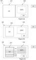
- FIGS. 2a to 2c represent different organizations of a rewritable non-volatile memory of a secure element to which one or more embodiments of the invention can be applied.
- a memory for example the NVM2 rewritable non-volatile memory 108 of the secure element 107, comprises a plurality of memory blocks, in which each memory block comprises a set of memory pages on which data can be written and/or deleted.
- memory page is used to designate the minimum unit for erasing data from the memory. Writing (also called “programming”) can be done on only part of a page.
- each memory card manufacturer provides a value called native endurance, which corresponds to the minimum endurance capacity assured for all memory pages on the card.
- native endurance For example, a native endurance of 10,000 cycles indicates that each memory page can withstand at least 10,000 write and erase cycles.
- Some memory pages can support endurance capacities much higher than this native endurance (here, 10,000 cycles), and there is great variability in the individual values of the endurance capacities of different memory pages.
- the NVM2 rewritable non-volatile memory 108 of the secure element 107 is organized as shown in the Figure 2a .
- the rewritable non-volatile memory 108 (for example, a Flash type memory) comprises two logical partitions defining two distinct memory zones: a first logical partition 201, called OS memory zone, named OS in the figure, dedicated to the storage of the system operating the secure element and a second logical partition 202, called data memory zone, named DATA in the figure, dedicated to the storage of other data, typically applications, profile and personalization data, data generated by applications, etc.
- the NVM2 rewritable non-volatile memory 108 of the secure element 107 comprises a single logical partition in which the operating system of the secure element and other data (applications, profiles, etc.) are stored.
- a first zone 203 called the OS memory zone, named OS in the figure, stores the operating system of the secure element while a second zone 204, called the data memory zone, named DATA in the figure, stores the others data and has sub-areas available for storing additional data.
- the data memory area can be the complement of the OS memory area in the NVM2 memory.
- Each area includes a plurality of memory pages (not shown on the Figures 2a-2b ).
- a memory page is made up of N contiguous bytes (N is typically a power of 2, for example 256, 512, 1024), the memory pages being contiguous within the NVM2 memory.
- the NVM2 memory of a secure element 107 can have a capacity of 512 kilobytes (kb) or 1024 kb.
- the size of the OS is for example 200 to 300 kb. In typical operation, the size of other data stored in the secure element is approximately 100 to 200 kb. However, this can fluctuate greatly depending on the uses of the secure element.
- the data memory zone 202 or 204 is advantageously partitioned into two logical sub-zones of memory pages: a working zone and a replacement zone (also called “endurance tank”, or “replacement tank” corresponding to the pages data memory not yet used).
- the work area includes a set of memory pages called “working pages” or “main pages”.
- a working page When a working page is identified as "worn”, its content is redirected to another page, either primary (if one is available) or replacement. For example, when new data needs to be written to a working page but it is worn out, its contents are copied to another page and the new data is written there. In one or more embodiments, the redirection of the content of the working page to another page is carried out using a pointer including the address of the new page. Furthermore, when such a new page is used in turn, its content is redirected to yet another page (main or replacement) not used.
- worn page is meant a memory page that has reached its endurance capacity and on which it is no longer possible to erase and/or write data correctly. It is noted that a memory page is “used” (ie the page has already been the subject of at least one write or erase) before being “used” (ie the maximum number of writes / erases has been reached for the page).
- a method for determining whether a memory page is worn or not is detailed in the patent FR 2 977 047 B1 and recalled afterwards.
- the card operating system is not or very little scalable over time. It is therefore conventional not to manipulate the OS memory area 201, 203 during the life of the secure element 107, with the exception of readings for loading the OS into RAM2 RAM2. Reusing OS memory pages as a stock of “healthy” memory pages to supplement is therefore not intuitive.
- the invention provides for determining whether at least one first data memory page is worn out, and if so, for moving the contents of the first used data memory page to an OS memory page while moving the contents from this OS memory page to a worn data memory page.
- the invention proposes, in one or more embodiments, to move, at once, the contents of the data memory pages of a block towards the first OS memory zone 201, 203, while moving the contents of the 'set of OS memory pages containing the entire operating system to data memory pages of data memory area 202 or 204.
- the operating system may have been compiled in the form of “relocatable” or “relocatable code” code in order to facilitate its movement within the NVM2 rewritable non-volatile memory.
- a code is said to be “delocalizable” or “relocalizable” when it can be loaded anywhere in the memory due to its independence of its position within the memory. This is particularly the case when using relative addresses.
- “Relocatable” or “relocalizable” code makes it possible in particular to break down the code into “independent” sections which can be loaded anywhere in the memory, and therefore be moved, independently of each other. However, any code referring to another section can be corrected using a relocation table (memorizing the offset); so sections can be linked together.
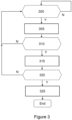
- FIG. 3 illustrates, using a flowchart, steps of a method of managing a rewritable non-volatile memory NVM2 according to one or more embodiments with global movement of the operating system.
- Such memory management can be implemented after exhaustion of the data memory pages as mentioned for example above.
- the movement of the contents of a used data memory page to the OS memory zone 201, 203 is conditional on the fact that the data memory zone 202, 204 no longer includes an unused data memory page or “healthy” that is free.
- step 300 the secure element is waiting for a write instruction in the data memory area 202, 204.
- write instruction is meant any instruction aimed at modifying data stored in a page data memory, therefore also including an erase instruction. Also, when such an instruction is received (“O” branch of step 300), it is executed in step 305, leading to writing on one or more data memory pages, depending on the size of the data to be write or erase. If the instruction received is not a write instruction (“N” branch of step 300), then the process loops back on itself at step 300 waiting for a new write instruction.
- step 310 a wear level of each of the “written” pages is determined.
- the process described in the patent FR 2 977 047 B1 can be used for this purpose.
- a “written” memory page may turn out to be worn out (“O” branch of step 310) in which case it is marked as such in step 315. Also, as the different writes to NVM2 memory progress, each “written” data memory page that is determined to be worn out is marked as such.
- the determined wear level is for example considered “worn” if it exceeds a preset wear threshold value THR1.
- THR1 a preset wear threshold value
- the marking may consist of the activation of a “used” flag associated with the memory page considered.
- a “worn” flag table for all data memory pages can be stored in a register 205 (illustrated in Figures 2a, 2b and 2c ), which could possibly be part of NVM2 memory.
- an identifier of the memory page (for example its address) can be stored in the register.
- ranges of identifiers (by storing the start page identifier and the end page identifier) may be stored to reduce the number of registers used.
- step 310 If no memory page is identified as newly worn (“branch “N” of step 310), then the process restarts at step 300 waiting for a new write instruction.
- the secure element determines in step 320 an overall wear rate of a block of data memory pages of the data memory area 202, 204, which includes the page(s) newly marked as worn.
- the question here is to determine whether a block in the data memory area 202, 204 is found to be too degraded, justifying a movement of its content to the OS memory area 201, 203.
- the block of data memory pages considered here is of equivalent size (e.g. the same size) as that of the OS memory area 201, 203. This aims to carry out, if necessary, a substitution of contents without leaving memory pages unused.
- the data memory area 202, 204 can be divided into N disjoint blocks of contiguous memory pages, each block being the size of the OS memory area 201, 203 with the possible exception of the last block.
- step 320 focuses on the block including the “written” memory page(s) newly marked as worn.
- the data memory area 202, 204 can be divided into M disjoint sub-blocks of one or more contiguous memory pages and of the same size (with the possible exception of the last block), this size being for example a submultiple of that of the OS memory area 201, 203.
- a sub-block therefore comprises a set of one or more contiguous memory pages.
- the block to be considered is made up of several consecutive disjoint sub-blocks.
- the block is therefore made up of several memory pages.
- Step 320 can then focus on all the blocks, each formed of several consecutive disjoint sub-blocks, which include the “written” memory page(s) newly marked as worn.
- the disjoint sub-blocks can be formed so as not to cut data stored on several consecutive memory pages.
- the overall wear rate may be representative of a number of worn data memory pages or a proportion of worn data memory pages in the block.
- the overall wear rate of the sector is Y/X.
- step 320 If several blocks are evaluated in step 320, only the one presenting the highest overall wear rate is considered.
- the overall wear rate of the block considered is compared to a threshold value, called the overall wear threshold, for example 90%.
- step 325 (branch “O” of step 320) aimed at moving the content of the data pages of this block towards the OS memory area 201, 203; otherwise (branch “N” of step 320), the process returns to step 300 waiting for a new instruction to write the NVM2 memory.
- Step 325 therefore consists of moving the content of the data memory pages of the block to the OS memory area 201, 203, while moving the content of all of the OS memory pages containing the entire operating system to data memory pages.
- this movement consists of the interversion (i.e. permutation or exchange) of the contents stored in the block of data memory pages with the contents stored in the OS memory zone 201, 203.
- the permutation of the contents can be on the fly, therefore immediately after step 320.
- Such a permutation, while the secure element 107 is in use, is possible because generally the operating system running has been loaded into RAM2 111. Also, it is possible to move the static compiled code from the operating system.
- step 320 it can first be planned in step 320, when it is determined that the contents of the block must be moved (because overall too worn), to mark this block as being to be moved. Again a flag associated with the block can be activated in register 205, or alternatively a block identifier can be stored.
- the movement step 325 is carried out when the secure element 107 is restarted.
- a step of checking whether a block of data memory pages is marked as being to be moved is carried out. If so, the secure element triggers the movement of the contents of the block of data memory pages marked as being to be moved to the OS memory area 201, 203.
- the restart can be left to the initiative of the user, for example when turning off the host device 100.
- the method according to the invention can trigger such a restart to force the movement of the contents.
- the restart instruction can be provided at the end of step 320.
- the triggering of the restart of the secure element is in response to the marking of the block of data memory pages as being to be moved.
- a backup memory 206 is available to allow movement.
- This memory may form part of NVM2 memory or not.
- NVM2 memory it can consist of a reserved area and therefore not used for data storage, or alternatively be made up of unworn and free memory pages of the data memory area 202, 204.
- the memory backup 206 can be of variable size depending on the number of free memory pages when step 325 is engaged.
- the contents can be moved in a single block, meaning that the backup memory 206 is of the same size as the block to be moved.
- the contents of the block of data memory pages to be moved are copied into the backup memory 206, then the contents of the OS memory area 201, 203, of size equivalent to that of the block of data memory pages. to be moved, is in turn copied into the memory pages forming said block whose content is already moved (so this OS content overwrites the old data content copied into backup memory 206), finally the content in backup memory 206 is copied into the memory pages of the OS memory area 201, 203.
- this can be the entire first zone, formed of the OS memory pages which is copied into backup memory 206.
- the backup memory 206 can be doubled and receive a copy of the two contents to be swapped , before inverted copies on the initial memory pages.
- the movement can be carried out in sub-blocks.
- a sub-block may in particular contain only one memory page (minimum unit).
- the movement is progressive: the first sub-block of the block to be moved and the first sub-block of the OS memory zone 201, 203 are interchanged using the backup memory 206, then the second sub-block of the block to be moved and the second sub-block of the OS memory area 201, 203 are interchanged, and so on.
- the backup memory 206 can be doubled to receive a copy of the two sub-blocks to be swapped.
- Moving the contents of memory pages (whether data memory pages or OS memory pages) requires updating the memory addresses corresponding to the various stored data.
- a memory management unit in a memory controller, not shown on the Figure 1 , maintains a correspondence table or “address translation table” translating the memory addresses sent by the processor CPU2 110 into physical addresses in the memory. Moving the contents of the memory pages modifies the physical address where the contents are stored. Also, when moving the contents of the data memory pages, the physical address of the address translation table is updated to point to the new address, corresponding to the destination OS memory pages in the OS memory area 201, 203.
- the operating system of a secure element generally includes, in hard copy at the start of the compiled code, an absolute memory address where this operating system is initially stored. In other words, this is the memory address starting the OS memory area 201, 203.
- the other addresses provided in the compiled code of the operating system are generally expressed as addresses relative to this absolute address.
- the operating system not being recompiled during the movement according to the invention, it is planned in one or more embodiments to update an indirection register to store information representative of a new memory address of the moved contents, here from the moved OS.
- This indirection register initially set to 0 during installation of the operating system, can include the memory shift or “offset” between the initial address and the destination address of the movement. The stored offset can simply be added to the addresses of loading.
- the call addresses to operating system functions are evaluated as being the sum of the initial absolute address of the OS, the relative address of the called function and the indirection value contained in the register, and therefore allow, before the move and after the move, to make calls to the functions of the operating system, without risk.
- step 325 the process ends.
- the operating system is now stored on a globally used block of memory pages. These therefore no longer constitute a reserve of “healthy” memory pages for a new implementation of the invention.
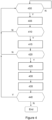
- FIG. 4 illustrates, using a flowchart, steps of a method for managing a rewritable non-volatile memory NVM2 according to one or more embodiments with progressive (or fragmented or piecemeal) movement of the operating system.
- the operating system can be “delocalizable” or “relocalizable” and thus be structured into sections that can be moved independently of each other, subject to updating the associated relocation table, as explained above.
- FIG 2c illustrates an operating system 207, named OS in the figure, structured in sections 208, in the memory configuration of the Figure 2b . It is also possible to use an operating system structured in sections 208, in the partitioned memory configuration of the Figure 2a .
- the stored operating system is therefore a compiled OS, composed of a plurality of sections capable of being stored independently, each being stored on a respective block of OS memory pages.
- the first OS section is stored on four memory pages (each horizontal strip schematically representing a memory page), the second section on two memory pages, etc.
- memory management according to Figure 4 can be implemented after exhaustion of the data memory pages as mentioned above.
- the movement of the contents of a used data memory page to an OS memory page (of zone 201, 203) is conditional on the fact that the data memory zone 202, 204 no longer includes an unused data memory page or " healthy” that is free.
- step 400 the secure element is waiting for a write instruction in the data memory area 202, 204, similarly to step 300 above.
- a write instruction in the data memory area 202, 204, similarly to step 300 above.
- it is executed in step 405 (similar to step 305), leading to writing on one or more data memory pages, depending on the size of the data to be written or erased.
- the instruction received is not a write instruction (“N” branch of step 400)
- the process loops back on itself at step 400 waiting for a new write instruction. With these steps 400 and 405, the rest of the process leading to the movement of contents of used memory pages is conditioned or "in response" to a step of writing data on a data memory page. Other conditions could nevertheless be used.
- step 410 similar to step 310 above, a level of wear of each of the “written” pages is determined. Again, the process described in the patent FR 2 977 047 B1 can be used for this purpose.
- a “written” memory page may turn out to be worn out (branch “O” of step 410) in which case it is marked as such in step 415. Also, as the different writes to NVM2 memory progress, each “written” data memory page that is determined to be worn out is marked as such.
- the determined wear level is for example considered “worn” if it exceeds a preset wear threshold value THR1.
- THR1 a preset wear threshold value
- the erasure quality measured by comparing the threshold voltages is lower than a wear threshold, then the memory page is considered worn (“worn state”).
- At least two different wear states can be evaluated for the memory page examined, depending on two respective threshold values.
- a first threshold value here the wear threshold value THR1 mentioned previously, makes it possible to assign the “worn” state to the memory page examined;
- a second threshold value THR2, called critical wear threshold value makes it possible to assign the “critical” state to the memory page examined.
- the “critical” state being more restrictive than the “worn” state, the threshold value THR2 is higher than the threshold value THR1 (“more high” in the sense of representing a greater level of wear, THR2 being able to be mathematically smaller than THR1).
- the marking mentioned may indicate “unworn”, “worn” or “critical”.
- a greater number of wear states can be used within the framework of the invention.
- the marking can then consist of the activation of a “used” flag or the indication of the state (“used” or “critical”) in a field associated with the memory page considered.
- This information can be stored in register 205, for each of the data memory pages, as explained above in step 315.
- an identifier of the page memory (for example its address) can be stored in the register as explained above in step 315.
- two registers, one associated with the “used” state and the other with the “critical” state can be used.
- step 410 If no memory page is identified as newly worn ("N" branch of step 410), then the process restarts at step 400 waiting for a new write instruction.
- the secure element determines at step 420 if the contents of this used memory page must be moved.
- the movement is systematic once the memory page is marked as worn.
- the movement is triggered if the memory page is marked as “critical”. Also, in these embodiments, reaching a particular wear rate of a data memory page worn beyond a critical threshold triggers the movement procedure.
- the movement is based on a type of data memory page associated with this used memory page.
- a type of data memory page associated with this used memory page.
- certain pages can be declared as unmovable (type 1 pages) because their content is sensitive (cryptographic keys, system area, base memory addresses, etc.). These pages can constitute a protected area of the NVM2 or be mixed with other data memory pages (in which case a marking makes it possible to identify them).
- the other data memory pages are subject to less protection and their contents can therefore be moved (type 2 pages).
- the movement is based on an overall wear rate of a set of data memory pages including the memory page(s) newly marked as worn.
- the secure element 107 can for example analyze one or more sets of contiguous data memory pages, each including the memory page(s) newly marked as worn, then evaluate an overall wear rate of each of these sets. This can for example make it possible to trigger the movement of the contents of a set of contiguous data memory pages including the first worn memory page, in the event of identification that this set of contiguous data memory pages has a higher overall wear rate. at an overall wear threshold.
- the overall wear rate may include a weighting of the Y/X ratio (described above at step 320, scaled to the set considered here) by the number of memory pages forming the set analyzed.
- the overall wear rate can be equal to Y/X 2 .
- the question here is to determine whether a sub-part of the data memory zone 202, 204 is found to be too degraded, justifying a movement of its contents to the OS memory zone 201, 203.
- step 420 If the overall wear rate of the assembly considered reaches the overall wear threshold (branch “O” of step 420), then the process continues in step 425 aimed at selecting one or more of the sections 208 of OS 207. If the overall wear rate of the assembly considered does not reach the overall wear threshold (branch “N” of step 420), then the process restarts at step 400 in waiting for a new write instruction.
- the selection referred to in step 425 consists of selecting the smallest set (in number of associated OS memory pages) of one or more contiguous sections of the OS having a size greater than the obtained set (in step 420) of data memory pages. We thus seek to identify the part of the OS memory area that is best suited (in terms of size) to the generally used memory pages to be moved.
- moving a memory page, moving a block, moving a section are to be understood in the sense of “moving the content” which is stored in the memory page(s) considered, in the block(s) considered or the section(s). considered.
- the optional step 430 consists of the secure element determining a final block of data memory page to be moved. This step is optional, because it can be decided to move only the set obtained in step 420 (possibly a single data memory page).
- the final block to be moved can for example be obtained by updating the set of data memory pages obtained in step 420, for example by adding neighboring data memory pages preceding and/or succeeding said set, depending on the selected OS section(s).
- the set of data memory pages is increased until it reaches the size of the OS section(s) selected in step 425.
- the data stored in this increased set is of course taken into account, in order not to not truncate them.
- the augmented assembly forming the final block has a size equivalent, possibly equal, to that of the selected OS section(s).
- step 430 Once the block of memory pages to be moved is obtained in step 430, its content is moved, during step 435, to the OS memory area 201, 203, typically by interchanging this content with that of the OS memory page block. corresponding to the selected section(s).
- the content stored on the selected section(s) is moved to one or more available data memory pages, preferably globally worn (according to an overall wear rate) different from the block of data memory pages (possibly the single memory page newly marked as worn) whose contents are moved in parallel.
- the permutation of the contents can be done on the fly, or during the next restart of the secure element (in which case a marking is put in place indicating when the block of memory pages obtained in step 430 is to be moved).
- the movement of contents can be done in a single block or in sub-blocks, depending on the size of the backup memory 206 available.
- the memory addresses are updated, typically in the address translation table for the data, and via the indirection register and/or the relocation table for the OS section(s) being moved
- step 440 may consist of checking whether there remains at least one unmoved OS section. Indeed, in this condition, there remains a reserve of “healthy” memory pages from which the invention could take advantage in order to extend the life of the NVM2 memory.
- step 440 returns to step 400 while waiting for a new write instruction. Otherwise (branch “N” of step 440), the process ends because there is no longer a reserve of “healthy” memory pages for a new implementation of the invention.
- the above description mainly envisages moving the contents of a data memory page to an OS memory page in order to benefit from the low wear of the latter. As long as there remain OS memory pages (or OS sections) that have not yet been moved, it is also possible to move data content already moved to an OS memory page again, to a new OS memory page if the first OS memory page turns out to be worn out (for example by multiple rewrites of the data it contains).
- the secure element determines that a first OS memory page to which the content of a used data memory page has already been moved, is worn out, and in response to this determination, moves said contents of this now used first OS memory page to a second OS memory page (the contents of which have not yet been moved).
- the invention therefore makes it possible to significantly extend the lifespan of a secure element.
- the proposed method and the equipment for implementing the method include different variants, modifications and improvements which will be obvious to those skilled in the art, it being understood that these different variants, modifications and improvements form part of the scope of the invention, as defined by the claims which follow.
- different aspects and characteristics described above can be implemented together, or separately, or substituted for each other. to others, and all of the different combinations and sub-combinations of aspects and characteristics are part of the scope of the invention. Additionally, some systems and equipment described above may not incorporate all of the modules and functions described for the preferred embodiments.
Landscapes
- Engineering & Computer Science (AREA)
- Theoretical Computer Science (AREA)
- Physics & Mathematics (AREA)
- General Engineering & Computer Science (AREA)
- General Physics & Mathematics (AREA)
- Techniques For Improving Reliability Of Storages (AREA)
- Memory System Of A Hierarchy Structure (AREA)
Applications Claiming Priority (1)
| Application Number | Priority Date | Filing Date | Title |
|---|---|---|---|
| FR2207787A FR3138536B1 (fr) | 2022-07-28 | 2022-07-28 | Procédé de gestion d’une mémoire d’un élément sécurisé |
Publications (1)
| Publication Number | Publication Date |
|---|---|
| EP4312128A1 true EP4312128A1 (de) | 2024-01-31 |
Family
ID=84330912
Family Applications (1)
| Application Number | Title | Priority Date | Filing Date |
|---|---|---|---|
| EP23185414.2A Pending EP4312128A1 (de) | 2022-07-28 | 2023-07-13 | Verfahren zur verwaltung eines speichers eines sicheren elements |
Country Status (2)
| Country | Link |
|---|---|
| EP (1) | EP4312128A1 (de) |
| FR (1) | FR3138536B1 (de) |
Citations (9)
| Publication number | Priority date | Publication date | Assignee | Title |
|---|---|---|---|---|
| EP1182669A2 (de) * | 2000-08-23 | 2002-02-27 | Sharp Kabushiki Kaisha | Nichtflüchtige Halbleiterspeicheranordnung |
| US20040057316A1 (en) * | 2002-09-25 | 2004-03-25 | Renesas Technology Corp. | Nonvolatile memory |
| US20070294490A1 (en) * | 2006-06-20 | 2007-12-20 | International Business Machines Corporation | System and Method of Updating a Memory to Maintain Even Wear |
| US20090172340A1 (en) * | 2007-12-28 | 2009-07-02 | Jian Tang | Methods and arrangements to remap non-volatile storage |
| WO2009100149A1 (en) * | 2008-02-10 | 2009-08-13 | Rambus, Inc. | Segmentation of flash memory for partial volatile storage |
| US20110271046A1 (en) * | 2008-10-28 | 2011-11-03 | Iyer Rahul N | Wear leveling for low-wear areas of low-latency random read memory |
| FR2977047A1 (fr) * | 2011-06-22 | 2012-12-28 | Starchip | Procede de gestion de l'endurance de memoires non volatiles. |
| US20130024609A1 (en) * | 2011-05-17 | 2013-01-24 | Sergey Anatolievich Gorobets | Tracking and Handling of Super-Hot Data in Non-Volatile Memory Systems |
| US20210019050A1 (en) * | 2019-07-15 | 2021-01-21 | Micron Technology, Inc. | Maintenance operations for memory devices |
-
2022
- 2022-07-28 FR FR2207787A patent/FR3138536B1/fr active Active
-
2023
- 2023-07-13 EP EP23185414.2A patent/EP4312128A1/de active Pending
Patent Citations (10)
| Publication number | Priority date | Publication date | Assignee | Title |
|---|---|---|---|---|
| EP1182669A2 (de) * | 2000-08-23 | 2002-02-27 | Sharp Kabushiki Kaisha | Nichtflüchtige Halbleiterspeicheranordnung |
| US20040057316A1 (en) * | 2002-09-25 | 2004-03-25 | Renesas Technology Corp. | Nonvolatile memory |
| US20070294490A1 (en) * | 2006-06-20 | 2007-12-20 | International Business Machines Corporation | System and Method of Updating a Memory to Maintain Even Wear |
| US20090172340A1 (en) * | 2007-12-28 | 2009-07-02 | Jian Tang | Methods and arrangements to remap non-volatile storage |
| WO2009100149A1 (en) * | 2008-02-10 | 2009-08-13 | Rambus, Inc. | Segmentation of flash memory for partial volatile storage |
| US20110271046A1 (en) * | 2008-10-28 | 2011-11-03 | Iyer Rahul N | Wear leveling for low-wear areas of low-latency random read memory |
| US20130024609A1 (en) * | 2011-05-17 | 2013-01-24 | Sergey Anatolievich Gorobets | Tracking and Handling of Super-Hot Data in Non-Volatile Memory Systems |
| FR2977047A1 (fr) * | 2011-06-22 | 2012-12-28 | Starchip | Procede de gestion de l'endurance de memoires non volatiles. |
| FR2977047B1 (fr) | 2011-06-22 | 2013-08-16 | Starchip | Procede de gestion de l'endurance de memoires non volatiles. |
| US20210019050A1 (en) * | 2019-07-15 | 2021-01-21 | Micron Technology, Inc. | Maintenance operations for memory devices |
Also Published As
| Publication number | Publication date |
|---|---|
| FR3138536B1 (fr) | 2025-03-28 |
| FR3138536A1 (fr) | 2024-02-02 |
Similar Documents
| Publication | Publication Date | Title |
|---|---|---|
| JP5696118B2 (ja) | 不揮発性メモリシステムのためのウィーブシーケンスカウンタ | |
| US8775758B2 (en) | Memory device and method for performing a write-abort-safe firmware update | |
| US20130219106A1 (en) | Trim token journaling | |
| US20050060699A1 (en) | Method and system for updating software | |
| US20090037648A1 (en) | Input/output control method and apparatus optimized for flash memory | |
| US9665496B2 (en) | Non-volatile memory write mechanism | |
| EP2302637A1 (de) | Verfahren zum Schreiben von Daten in einen nichtflüchtigen Speicher, der gegen Herausreißen geschützt ist | |
| US9710340B2 (en) | Replacement of a corrupt driver variable record | |
| US7222214B2 (en) | Device-level address translation within a programmable non-volatile memory device | |
| EP2724237B1 (de) | Verfahren zur verwaltung der robustheit von nichtflüchtigen speichern | |
| KR100698655B1 (ko) | 이동통신 단말기의 파일 업데이트 시스템과, efs 영역헤더 손실로 인한 치명적인 에러를 방지하는 이동통신단말기의 부팅 관리 시스템과, 이동통신 단말기의 파일업데이트 방법 및 efs 영역 헤더 손실로 인한 치명적인에러를 방지하는 이동통신 단말기의 부팅 방법 | |
| CN111597066A (zh) | Ssd修复方法、装置、计算机设备及存储介质 | |
| EP4312128A1 (de) | Verfahren zur verwaltung eines speichers eines sicheren elements | |
| KR100677227B1 (ko) | 이동단말기의 갱신속도 개선 방법 | |
| KR101676175B1 (ko) | 전원 손실 이후 데이터 손실을 방지하기 위한 메모리 저장 장치 및 방법 | |
| CN1977244A (zh) | 安全闪存 | |
| WO2003027851A1 (fr) | Procede et dispositif de verifieur de code optimise | |
| FR3074317B1 (fr) | Procede d'acces a une zone memoire non volatile de type flash d'un element securise, tel qu'une carte a puce | |
| FR3125897A1 (fr) | Procédé pour optimiser un fonctionnement d’un élément sécurisé | |
| KR20060068558A (ko) | 휴대 단말기를 위한 펌웨어 업그레이드 방법 | |
| CN114546463A (zh) | 一种软件更新方法及装置 | |
| US20030237021A1 (en) | Automatic restoration of software applications in a mobile computing device | |
| CN110262916B (zh) | 系统码的管理装置及其管理方法 | |
| JP2014115927A (ja) | プログラム更新装置、方法、プログラム、及び記憶媒体 | |
| KR20100001741A (ko) | 불휘발성 메모리를 포함하는 이레이저 시스템 및 그것의구동방법 |
Legal Events
| Date | Code | Title | Description |
|---|---|---|---|
| PUAI | Public reference made under article 153(3) epc to a published international application that has entered the european phase |
Free format text: ORIGINAL CODE: 0009012 |
|
| STAA | Information on the status of an ep patent application or granted ep patent |
Free format text: STATUS: REQUEST FOR EXAMINATION WAS MADE |
|
| 17P | Request for examination filed |
Effective date: 20230713 |
|
| AK | Designated contracting states |
Kind code of ref document: A1 Designated state(s): AL AT BE BG CH CY CZ DE DK EE ES FI FR GB GR HR HU IE IS IT LI LT LU LV MC ME MK MT NL NO PL PT RO RS SE SI SK SM TR |
|
| P01 | Opt-out of the competence of the unified patent court (upc) registered |
Free format text: CASE NUMBER: APP_23806/2025 Effective date: 20250519 |
|
| RAP1 | Party data changed (applicant data changed or rights of an application transferred) |
Owner name: IDEMIA FRANCE |
|
| GRAP | Despatch of communication of intention to grant a patent |
Free format text: ORIGINAL CODE: EPIDOSNIGR1 |
|
| STAA | Information on the status of an ep patent application or granted ep patent |
Free format text: STATUS: GRANT OF PATENT IS INTENDED |
|
| INTG | Intention to grant announced |
Effective date: 20260309 |