EP4315533B1 - Circuit d'allumage de diodes lasers - Google Patents
Circuit d'allumage de diodes lasers Download PDFInfo
- Publication number
- EP4315533B1 EP4315533B1 EP22716915.8A EP22716915A EP4315533B1 EP 4315533 B1 EP4315533 B1 EP 4315533B1 EP 22716915 A EP22716915 A EP 22716915A EP 4315533 B1 EP4315533 B1 EP 4315533B1
- Authority
- EP
- European Patent Office
- Prior art keywords
- current
- shunt
- laser diode
- circuit
- lasing
- Prior art date
- Legal status (The legal status is an assumption and is not a legal conclusion. Google has not performed a legal analysis and makes no representation as to the accuracy of the status listed.)
- Active
Links
Images

Classifications
-
- H—ELECTRICITY
- H01—ELECTRIC ELEMENTS
- H01S—DEVICES USING THE PROCESS OF LIGHT AMPLIFICATION BY STIMULATED EMISSION OF RADIATION [LASER] TO AMPLIFY OR GENERATE LIGHT; DEVICES USING STIMULATED EMISSION OF ELECTROMAGNETIC RADIATION IN WAVE RANGES OTHER THAN OPTICAL
- H01S5/00—Semiconductor lasers
- H01S5/04—Processes or apparatus for excitation, e.g. pumping, e.g. by electron beams
- H01S5/042—Electrical excitation ; Circuits therefor
-
- H—ELECTRICITY
- H01—ELECTRIC ELEMENTS
- H01S—DEVICES USING THE PROCESS OF LIGHT AMPLIFICATION BY STIMULATED EMISSION OF RADIATION [LASER] TO AMPLIFY OR GENERATE LIGHT; DEVICES USING STIMULATED EMISSION OF ELECTROMAGNETIC RADIATION IN WAVE RANGES OTHER THAN OPTICAL
- H01S5/00—Semiconductor lasers
- H01S5/06—Arrangements for controlling the laser output parameters, e.g. by operating on the active medium
- H01S5/0607—Arrangements for controlling the laser output parameters, e.g. by operating on the active medium by varying physical parameters other than the potential of the electrodes, e.g. by an electric or magnetic field, mechanical deformation, pressure, light, temperature
- H01S5/0608—Arrangements for controlling the laser output parameters, e.g. by operating on the active medium by varying physical parameters other than the potential of the electrodes, e.g. by an electric or magnetic field, mechanical deformation, pressure, light, temperature controlled by light, e.g. optical switch
-
- H—ELECTRICITY
- H01—ELECTRIC ELEMENTS
- H01S—DEVICES USING THE PROCESS OF LIGHT AMPLIFICATION BY STIMULATED EMISSION OF RADIATION [LASER] TO AMPLIFY OR GENERATE LIGHT; DEVICES USING STIMULATED EMISSION OF ELECTROMAGNETIC RADIATION IN WAVE RANGES OTHER THAN OPTICAL
- H01S5/00—Semiconductor lasers
- H01S5/06—Arrangements for controlling the laser output parameters, e.g. by operating on the active medium
- H01S5/068—Stabilisation of laser output parameters
- H01S5/06825—Protecting the laser, e.g. during switch-on/off, detection of malfunctioning or degradation
-
- H—ELECTRICITY
- H01—ELECTRIC ELEMENTS
- H01S—DEVICES USING THE PROCESS OF LIGHT AMPLIFICATION BY STIMULATED EMISSION OF RADIATION [LASER] TO AMPLIFY OR GENERATE LIGHT; DEVICES USING STIMULATED EMISSION OF ELECTROMAGNETIC RADIATION IN WAVE RANGES OTHER THAN OPTICAL
- H01S5/00—Semiconductor lasers
- H01S5/06—Arrangements for controlling the laser output parameters, e.g. by operating on the active medium
- H01S5/068—Stabilisation of laser output parameters
- H01S5/0683—Stabilisation of laser output parameters by monitoring the optical output parameters
-
- H—ELECTRICITY
- H01—ELECTRIC ELEMENTS
- H01S—DEVICES USING THE PROCESS OF LIGHT AMPLIFICATION BY STIMULATED EMISSION OF RADIATION [LASER] TO AMPLIFY OR GENERATE LIGHT; DEVICES USING STIMULATED EMISSION OF ELECTROMAGNETIC RADIATION IN WAVE RANGES OTHER THAN OPTICAL
- H01S5/00—Semiconductor lasers
- H01S5/40—Arrangement of two or more semiconductor lasers, not provided for in groups H01S5/02 - H01S5/30
- H01S5/4018—Lasers electrically in series
-
- H—ELECTRICITY
- H01—ELECTRIC ELEMENTS
- H01S—DEVICES USING THE PROCESS OF LIGHT AMPLIFICATION BY STIMULATED EMISSION OF RADIATION [LASER] TO AMPLIFY OR GENERATE LIGHT; DEVICES USING STIMULATED EMISSION OF ELECTROMAGNETIC RADIATION IN WAVE RANGES OTHER THAN OPTICAL
- H01S5/00—Semiconductor lasers
- H01S5/40—Arrangement of two or more semiconductor lasers, not provided for in groups H01S5/02 - H01S5/30
- H01S5/42—Arrays of surface emitting lasers
- H01S5/423—Arrays of surface emitting lasers having a vertical cavity
Definitions
- This invention relates to semiconductor lasers used in lighting applications.
- Laser diodes are known for their reliable operation with enormous brightness and high quality of light.
- White laser-based light sources have also recently become available. They typically employ a blue laser diode combined with a phosphor converter adding yellow components to the blue laser light resulting in a white light with CRI (Color rendering index) of about 70.
- CRI Color rendering index
- laser diodes are susceptible to damage. Operating frequencies may exceed 1 GHz and, in addition to this, laser diodes are low voltage devices that are typically operated at 2-3 volts. The combination of these two factors make them very susceptible to surge-damage.
- Laser diodes are so responsive at high frequencies that they are easily damaged by transients with relatively little energy content. This is especially true when they are operated near to their nominal power, and the headroom for any overheating effects is very limited.
- Overvoltage such as due to glitches in the supply or ESD (Electro-Static Discharge) damage the semiconductor layers.
- Over-temperature can also directly damage or lead to a thermal runaway, as the threshold voltage and impedance change.
- multiple laser diodes are bundled in one housing as a laser diode bank.
- the individual laser diodes may be connected in series (as a laser diode string) by means of a printed circuit board (PCB) and they can be powered from a common connector from a single shared driver.
- PCB printed circuit board
- multiple strings of laser diodes may be electrically connected in parallel.
- This invention relates, in particular, to the control of such bundled laser diode packs.
- the laser diodes of the bundled laser diode pack are for example powered up together. This has several implications, for example the laser diodes cannot individually be controlled nor protected.
- the voltage division between the laser diodes is heavily dependent on the rate of change of current and the individual laser parameters, and this voltage division cannot be controlled. It is also not possible to address overvoltage issues at the level of the individual laser diodes when there is only a single connector or driver.
- stray inductances as well as stray capacitances can severely influence the division of the overall string voltage between the individual laser diodes.
- impedance of a laser diode changes at the moment it starts lasing, which substantially influences the voltage as seen over individual laser diode devices during the current ramp up.
- US 2014/0226688 discloses a driver for series connected loads, each having a laser diode.
- a shunt device is connected in parallel with at least one of the loads to reduce a DC pump current to the load.
- the shunt device means that different loads in series connection can be driven at different DC drive currents.
- WO 2014/208048 discloses a laser diode driver which is provided with a driving means which, in response to the output state of a plurality of laser diodes connected in series between two power sources, controls the driving of a prescribed laser diode.
- the driving means includes a current control means taking as an input a signal corresponding to the output of an individual laser diode and controlling the current supplied to the individual laser diode in response to the input signal, a current path control means for controlling the current control means in response to the input signal, and a laser diode control means for controlling the current supplied between the power sources in response to the input signal.
- a lighting circuit comprising:
- This lighting circuit makes use of local circuitry shunting the current away from one or more selected laser diodes.
- These laser diodes are in particular the ones which start lasing earlier than others (because of the slightly different device characteristics of the laser diodes). For devices for which a high current is needed before lasing starts, the current shunting may not be required and is thus not activated.
- the circuit in particular addresses the issue that high frequency components can result in crystal damage as discussed above, and these high frequency components may be generated when neighboring lasers start to lase.
- a laser e.g. LD1
- another laser e.g. LD2
- the voltage drop over LD2 will suddenly change. This influences the voltage division in the series connection, and as a consequence results in additional current insertion at LD1. This gives the risk of inducing a failure mechanism as discussed above.
- the ability to control current transients reduces that risk.
- VCSEL vertical cavity surface emitting laser
- This approach reduces driving effort for laser diode arrays. It provides a low effort solution when compared to active current shifting, and it may be used to make sure all laser diodes start lasing at the same moment when switched on. It may also be used to provide pixelated laser diode addressing in a simple way. This is possible by simply shunting all the current around a laser generated pixel to keep it off. These shunting elements do not need to be big and/or complex.
- the control arrangement may operate local control, whereby the control of a current shunt circuit is determined based on the current and/or voltage at the respective laser diode, or there may be centralized control, whereby a central control system knows the timing of the start of lasing of all of the laser diodes and controls them all in dependence on the overall circuit response.
- the lasers can be driven in order, by delaying the lasers with a low laser threshold current to make sure that they all start lasing synchronously. This helps as the voltage change during the start of lasing will not initiate current spikes in other devices which are already at nominal lasing (as they all start synchronously). In an optimal system, the voltage drops of all lasers will be synchronized and the voltage division will not be influenced. As a result, each laser diode can be made to start lasing, based on the current reaching the laser threshold level, at a desired time.
- the invention in particular aims to use the shunt switch during the moment in time that the associated laser diode starts to operate in lasing mode. During the transition time to lasing, a steep negative rate of change of voltage occurs. This is caused by the current flowing through the laser diodes.
- the current shunt circuit is used to reduce the current through the laser diode so that the rate of change of voltage is reduced.
- the lighting circuit may further comprise a filter across the output terminals of the current drive circuit.
- Filtering for example by means of a capacitor, keeps operation conditions at the laser diode string free of ringing and high frequency components.
- the filter can prevent the string voltage from varying rapidly.
- the lighting circuit may further comprise a voltage sensor for sensing a forward voltage of each laser diode.
- the control arrangement may for example be adapted to control the level of the shunt currents such that each laser diode has a same forward voltage during the start-up period of time. Thus, the voltage division is made uniform.
- the lighting circuit may further comprise a monitor for detecting the start of lasing of each laser diode, wherein the controller is adapted to control the shunt circuit based on the monitored start of lasing.
- Laser diodes which will start lasing at a low current can thus be delayed so that the lasing takes place at the same time, and the voltage division remains uniform during the start of lasing.
- the monitor may comprise a voltage monitor for monitoring a forward voltage of each laser diode and a current monitor for monitoring a laser diode current. In combination, this provides one way to detect lasing based on the electrical parameters of the laser diode.
- the monitor may instead comprise a light detector for monitoring a light output of each laser diode. This provides an alternative way to detect lasing based on an external light monitor.
- the control arrangement may be adapted to delay the start of lasing of selected laser diodes such that all laser diodes start lasing closer together in time. They may ideally all start lasing at the same time.
- the control arrangement may be adapted to control the level of the shunt currents after the start-up period of time by ramping down to a zero shunt current. This minimizes losses in the current sourcing components.
- the control arrangement may also be adapted to control the level of the shunt currents after the start-up period of time for setting non-equal currents through the laser diodes.
- These non-equal currents may for example be used to provide color point control when different laser diodes have different output colors.
- the control arrangement may be adapted to control the level of the shunt currents after the start-up period of time by increasing a shunt current in response to a detected light output above a threshold. This may be used in order to stabilize the laser output and protect against the COD as discussed above.
- the lighting circuit may further comprise:
- the control arrangement may comprise a central controller which connects to each current shunt circuit.
- control arrangement may comprise a set of distributed controller units, each associated with a respective current shunt circuit.
- Each current shunt circuit then has a separate controller which may uses observation circuitry for the laser diode behavior to control the shunting.
- Each laser diode and associated current shunt may comprise a module within a single housing.
- the invention also provides a laser diode module for use in the lighting circuit defined above, wherein the laser diode module comprises:
- the invention provides a lighting circuit comprising a current driver circuit and a series connection of at least two laser diodes, supplied with current from the current driver circuit.
- a current shunt circuit is in parallel with each laser diode for diverting a shunt current away from the respective laser diode.
- the level of the shunt currents is controlled during a start-up period of time of the current driver circuit in order to control the rate of change of voltage across selected laser diodes.
- Figure 1 shows a lighting circuit 10 comprising a current driver circuit 12 which connects to a lighting unit 14 for example over a twisted pair cable 16.
- the current driver circuit 12 delivers a regulated lighting string current I LSt .
- the current level is for example controlled based on an external control input to the current driver.
- the driver for example comprises a switch mode power supply.
- the string current may be a DC current (with different possible analogue current levels) or it may be a PWM current with constant current level.
- the PWM frequency needs to take account of the slopes of the current rise edges.
- the lighting unit 14 comprises a series connection of at least two laser diodes, for example laser diodes 20 1 to 20 8 and they are supplied with the string current I Lst from the current driver circuit 12.
- Each laser diode has a respective current shunt circuit 22 1 to 22 8 in parallel with the laser diode for diverting a shunt current (which is a portion or all of the string current I Lst ) away from the respective laser diode.
- Figure 1 shows an example with a central control arrangement 30 for controlling the current shunt circuits 22 1 to 22 8 .
- monitor unit 24 for generating feedback information to the control arrangement 30 for use in controlling at least the timing but preferably also the current level of the shunt current of each current shunt circuit 22 1 to 22 8 .
- the levels of the shunt currents are in particular controlled during a start-up period of time of the current driver circuit 12 during which the output of the current driver circuit 12 ramps from zero to a drive current.
- This level may be controlled as on or off, or it may be controlled as selected one of a multi-level signal, or it may be controlled as an analog current level.
- the aim is to reduce a rate of change of voltage across selected laser diodes during the start-up period of time, and thereby reduce the risk of damage to the laser diodes.
- the shunt control takes place when the laser diode starts to operate in lasing mode.
- the shunt control takes place when the laser diode starts to operate in lasing mode.
- there is a rise in forward voltage for a laser diode when it starts to lase and this in turn causes the other laser diodes in series to experience a step down in forward voltage.
- lasing (of the other laser diodes) may not start or may be cut off momentarily which can cause disastrous oscillations between two or more laser diodes.
- this leads to a delayed lasing for the other laser diodes in series with a higher lasing threshold current.
- the first laser diode may then reach full power by the time the others start lasing. This increases the risk of small overshoots due to noise in the current (e.g. because there are stray inductances reacting to the voltage steps and/or oscillations, or because the control in the driver tries counteracting for the spurious output voltage changes and overreacts).
- the photon headroom may then be exceeded causing facet destruction.
- the current shunt circuits are used to reduce the current through the laser diodes so that the rate of change of voltage is reduced.
- the current shunt circuits may for example be mounted on the backside of a PCB which carries the array of laser diodes.
- the current shunt circuits are shown as controllable current sources.
- the current through each of the laser diodes 20 1 -20 8 is reduced by enabling the associated current shunt circuit.
- the monitor 24 in this example is a light detector. It is used to inform the control arrangement 30 of the start of lasing of each individual laser diode.
- the current driver circuit 12 supplies the circuit by means of two conductors 16 with the string current I LSt .
- a filter such as a capacitor 40
- the capacitor 40 keeps the overall string voltage U LSt from varying rapidly.
- the filter is across the output terminals of the current drive circuit 12 and preferably at the location of the laser diodes.
- the use of the filter has the side-effect that the impedance change which arises when the first laser diode starts to lase will influence the voltage division over the string of series connected laser diodes. This will have an influence on the start of lasing in the other laser diodes.
- each of the eight laser diodes has a forward voltage of 1/8 U LSt .
- the control arrangement is able to dynamically balance the voltage division between all laser diodes, since all laser diode voltages can be monitored centrally.
- Each laser diode may then include a voltage sensor (not shown in Figure 1 ) so that the control arrangement can monitor the voltages at each node along the series chain.
- the effect of equilibrating the voltages across the laser diodes is to make them all lase at the same time. This is achieved by keeping early lasing diodes (ones with a low threshold current) at a low lasing status until all laser diodes are starting to lase. The lasing power in all laser diodes will thereby be low when any spurious currents due to the start of lasing may occur. In this way, no fatal overheating failures occur.
- the shunt currents may be smoothly brought back to zero, in order to allow each laser diode to start lasing at its individual lasing threshold.
- the destructive mechanisms act in microseconds, so the shunt currents may be relaxed after a short time period, for example in the range 10 to 1000 ⁇ s.
- One result of the current shunting function is that the rising current edges become flattened. This has to be taken into account when setting the maximum PWM rate for the laser bank.
- An external control signal may be used to influence the current division between individual laser diodes when they are being operated in their steady state (i.e. after the start-up period). This may be achieved by controlling the level of the shunt currents after the start-up period, for setting non-equal currents through the laser diodes. This may be used for example to set a specific color point in systems with multiple spectra coming from laser diodes with different color points.
- FIG. 1 shows an optional series switch 50 which allows the deactivation of the whole string in the case of over voltage or over current conditions.
- a voltage monitor for monitoring a forward voltage of each laser diode
- a current monitor for monitoring a laser diode current.
- this may allow the use of simple (LED grade) current drivers to supply the laser diode string.
- FIG. 1 shows a centralized control arrangement 30. Instead, the control arrangement may be distributed. Each current shunt circuit then has a separate controller which uses observation circuitry for the laser diode behavior to control the shunting.
- One way to control the shunting is by means of light flux observation as discussed above, using the monitor 24.
- the current source may then be directly controlled based on the flux emitted. If there is no flux, there is no need for current shunting. If there is a lasing flux, the current shunting is enabled.
- the shunting may start when lasing starts with a fixed shunting current, and then ramp automatically down to zero. This gives any filters (parasitic or designed) in the laser string supply sufficient time to discharge. This is particularly relevant as the laser diode string has a lower supply voltage than the string before start of lasing.
- Shunting current away from the laser diodes when the flux rises above a nominal value may also be used in order to stabilize the laser output and protect against thermal runaway in the resonating crystal.
- the monitoring of the forward voltage of the laser diodes may also be used to compensate for the drop in impedance as reported by Feng, Liefeng et. al: "Sudden Change of Electrical Characteristics at Lasing Threshold of a Semiconductor Laser”; Quantum Electronics, IEEE Journal of. 43. 458 - 461. 2007 .
- the current shunting does not require any access to or change in the optical path.
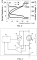
- Figure 2 is repeated from this reference. It shows the resistance and junction voltage as a function of current for two different laser diodes.
- the lasing threshold in each case is around 30mA.
- the measurements show that at the start of lasing, the laser diode impedance falls.
- a drop in the forward voltage might be expected in response to the drop in impedance, but instead there is a step increase in the forward voltage, as mentioned above.
- the junction voltage jumps abruptly to a saturated value at the onset of lasing. Electrically, the input power increases at this time, corresponding to the increase in optical output power at lasing.
- the voltage jump can be explained as a reaction inside the laser crystal when the number of photons is rising due to lasing, which reduces the recombination rate of electrons generating photons.
- This voltage behavior is directly related to the start of lasing.
- the effect is explained in Feng as being caused by a photo diode effect resulting from high photon density in the lasing layer.
- the amplitude of the voltage jump can be used to steer the current to be shunted away from the laser diode in order to enable the voltage to remain steady as seen from the outside or driver side.
- the monitor for detecting the start of lasing may comprise a voltage monitor for monitoring a forward voltage of each laser diode and a current monitor for monitoring a laser diode current.
- control arrangement may be distributed.
- Figure 3 shows a single laser diode 20 and its associated current shunt circuit 22, as a well as a local control circuit 70.
- the forward voltage is obtained using a measurement amplifier 72 which obtains a voltage difference between the anode and cathode of the laser diode 20.
- a current sensor 74 provides sensing of the string current to the local control circuit.
- the controller 70 When the voltage jumps without a related jump in the string current I LSt the controller 70 operates the current switching circuit 22 to carry as much current I Snt as required to compensate for the jump. In this way, the protection method involves slowing down the start of lasing by stealing current from the laser diode when lasing commences. The dynamics in the series connection are thereby reduced. Each laser diode will then start lasing at its respective individual lasing threshold current, but the lasing increase will be moderated.
- the individual lasing threshold current can be measured by the controller as it is the current when the voltage starts jumping.
- the shunting circuitry as well as the controller and the measurement circuitry may be supplied with power by scavenging from the voltage U LD over the laser diode 20. It will hence not consume power when the laser is off.
- the shunt currents will be controlled at each PWM rising edge.
- Typical PWM duty cycles for LED lighting are above 400Hz. High frequency operation around or above 20kHz is also used to prevent audible noise.
- the influence of a slowdown of the rising edge of ones or tens of microseconds can already cause visible distortions, as the full cycle is then only 50 ⁇ s. Therefore, the PWM frequency in this application is typically in the range 400 Hz to 1000 Hz.
- a delay of the current ramp-up time may be at most 100 ⁇ s, allowing for minimally distorted PWM of about 250Hz-400Hz.
- the current shunt circuit may be integrated with the laser diode in a single housing as the current shunt circuit does not need to be large or complex. If no external control is needed and only smooth voltage transitions are desired, a simple measurement analog circuit may be used. This can be integrated on a single die so integration in a laser diode housing is viable. Such an integrated protection circuitry does not require any additional housing pins or wires.
- the current shunting may be used to stabilize color or color temperature in a multi laser diode system with multiple spectral contributions.
- the circuit may also be applied for the selective driving of individual laser diode sources in one string as individual pixels. This is possible by simply shunting all the current around a pixel to keep it off. The smooth current takeovers can be guaranteed by soft adjustments of the current sources in order to omit any ringing or risking over voltage at the other pixels.
- control of the current shunt circuits may be guided by external parameters such as the temperature of the cooling aid of the laser diode arrangement.
- the lasing threshold for each laser diode may be calibrated over the typical temperature range. Feed forward calculations can compensate for the temperature difference between the cooling aid temperature and the semiconductor temperature.
- the monitoring unit (e.g. for monitoring the total flux generated by the bank of laser diodes) may be used to check whether the lasing threshold is as expected from calibration. It may be recalibrated during its lifetime whenever substantial differences to the calibration are detected. Auto-calibration may be supported e.g. during power up / power-down cycles when required. For these auto-calibration functions, the current slope may be slow to allow accurate measurements.
- the invention is for example of particular interest for spotlight applications, e.g. in museums and retail, multi-color laser applications like projection and city beautification, and for structured light laser projection.
Landscapes
- Physics & Mathematics (AREA)
- Condensed Matter Physics & Semiconductors (AREA)
- General Physics & Mathematics (AREA)
- Electromagnetism (AREA)
- Optics & Photonics (AREA)
- Semiconductor Lasers (AREA)
- Circuit Arrangement For Electric Light Sources In General (AREA)
Claims (13)
- Circuit d'éclairage (10) comprenant :un circuit d'attaque de courant (12) ;une connexion en série d'au moins deux diodes laser (20), alimentées en courant par le circuit d'attaque de courant ;un circuit en dérivation de courant respectif (22) en parallèle avec chaque diode laser pour détourner un courant en dérivation de la diode laser respective ; etun agencement de commande (30) pour commander les circuits en dérivation de courant, dans lequel l'agencement de commande est conçu pour :commander un niveau des courants en dérivation pendant une période de temps de démarrage du circuit d'attaque de courant, pendant laquelle la sortie du circuit d'attaque de courant passe de zéro à un courant d'attaque, réduisant ainsi un taux de changement de tension aux bornes de diodes laser sélectionnées pendant ladite période de temps de démarrage,caractérisé en ce que le circuit d'éclairage (10) comprend en outre un moniteur (24) pour détecter le début de l'activité laser de chaque diode laser, dans lequel l'agencement de commande est conçu pour commander le circuit en dérivation sur la base du début surveillé de l'activité laser.
- Circuit d'éclairage selon la revendication 1, comprenant en outre un filtre (40) à des bornes de sortie du circuit d'attaque de courant.
- Circuit d'éclairage selon la revendication 1 ou 2, comprenant en outre un capteur de tension (72) pour détecter une tension directe de chaque diode laser.
- Circuit d'éclairage selon la revendication 3, dans lequel l'agencement de commande (30) est conçu pour commander le niveau des courants en dérivation de telle sorte que chaque diode laser ait une même tension directe pendant la période de temps de démarrage.
- Circuit d'éclairage selon la revendication 1, dans lequel le moniteur comprend un moniteur de tension (72) pour surveiller une tension directe de chaque diode laser et un moniteur de courant (74) pour surveiller un courant de diode laser.
- Circuit d'éclairage selon la revendication 1, dans lequel le moniteur comprend un détecteur de lumière (24) pour surveiller une sortie de lumière de chaque diode laser.
- Circuit d'éclairage selon l'une quelconque des revendications 1 à 6, dans lequel l'agencement de commande (30) est conçu pour retarder le début de l'activité laser de diodes laser sélectionnées de telle sorte que toutes les diodes laser débutent leur activité laser de manière plus rapprochée dans le temps.
- Circuit d'éclairage selon l'une quelconque des revendications 1 à 7, dans lequel l'agencement de commande (30) est conçu pour commander le niveau des courants en dérivation après la période de temps de démarrage en diminuant progressivement jusqu'à un courant en dérivation nul.
- Circuit d'éclairage selon l'une quelconque des revendications 1 à 7, dans lequel l'agencement de commande (30) est conçu pour commander le niveau des courants en dérivation après la période de temps de démarrage pour établir des courants non égaux entre les diodes laser.
- Circuit d'éclairage selon l'une quelconque des revendications 1 à 9, dans lequel l'agencement de commande (30) est conçu pour commander le niveau des courants en dérivation après la période de temps de démarrage en augmentant un courant en dérivation en réponse à une sortie de lumière détectée au-dessus d'un seuil.
- Circuit d'éclairage selon l'une quelconque des revendications 1 à 10, comprenant en outre :un commutateur série (50) en série avec la connexion en série d'au moins deux diodes laser ; etun circuit de détection pour détecter une surtension ou une surintensité et commander le commutateur série en réponse à cela.
- Circuit d'éclairage selon l'une quelconque des revendications 1 à 11, dans lequel l'agencement de commande comprend :un dispositif de commande central (30) qui se connecte à chaque circuit en dérivation de courant ; ouun ensemble d'unités de commande distribuées (70), chacune associée à un circuit en dérivation de courant respectif.
- Circuit d'éclairage selon l'une quelconque des revendications 1 à 12, dans lequel chaque diode laser et dérivation de courant associée comprennent un module au sein d'un boîtier unique.
Applications Claiming Priority (2)
| Application Number | Priority Date | Filing Date | Title |
|---|---|---|---|
| EP21166068 | 2021-03-30 | ||
| PCT/EP2022/057271 WO2022207377A1 (fr) | 2021-03-30 | 2022-03-21 | Circuit d'éclairage à diodes laser |
Publications (2)
| Publication Number | Publication Date |
|---|---|
| EP4315533A1 EP4315533A1 (fr) | 2024-02-07 |
| EP4315533B1 true EP4315533B1 (fr) | 2024-11-20 |
Family
ID=75302406
Family Applications (1)
| Application Number | Title | Priority Date | Filing Date |
|---|---|---|---|
| EP22716915.8A Active EP4315533B1 (fr) | 2021-03-30 | 2022-03-21 | Circuit d'allumage de diodes lasers |
Country Status (5)
| Country | Link |
|---|---|
| US (1) | US20240162680A1 (fr) |
| EP (1) | EP4315533B1 (fr) |
| JP (1) | JP7522942B2 (fr) |
| CN (1) | CN117099276A (fr) |
| WO (1) | WO2022207377A1 (fr) |
Families Citing this family (1)
| Publication number | Priority date | Publication date | Assignee | Title |
|---|---|---|---|---|
| CN117074836B (zh) * | 2023-10-12 | 2024-03-12 | 成都明夷电子科技有限公司 | 一种激光器检测方法、检测器、电子设备及存储介质 |
Family Cites Families (6)
| Publication number | Priority date | Publication date | Assignee | Title |
|---|---|---|---|---|
| US7701990B2 (en) * | 2004-12-08 | 2010-04-20 | Mitsubishi Denki Kabushiki Kaisha | Laser diode pumped solid-state laser oscillator and laser diode control method of the oscillator |
| US10264637B2 (en) | 2009-09-24 | 2019-04-16 | Cree, Inc. | Solid state lighting apparatus with compensation bypass circuits and methods of operation thereof |
| US20140226688A1 (en) | 2013-02-11 | 2014-08-14 | Raytheon Company | Multiple output diode driver with independent current control and output current modulation |
| WO2014208048A1 (fr) | 2013-06-24 | 2014-12-31 | 日本電気株式会社 | Pilote de diode laser, dispositif d'amplification de lumière directe, système de transmission de signal lumineux et procédé de pilotage de diode laser |
| JP6283542B2 (ja) | 2014-03-14 | 2018-02-21 | 株式会社小糸製作所 | 車両用灯具およびその駆動装置 |
| WO2017168565A1 (fr) * | 2016-03-29 | 2017-10-05 | 三菱電機株式会社 | Module source de lumière laser, dispositif source de lumière et procédé de spécification de la défaillance d'une diode laser |
-
2022
- 2022-03-21 EP EP22716915.8A patent/EP4315533B1/fr active Active
- 2022-03-21 WO PCT/EP2022/057271 patent/WO2022207377A1/fr not_active Ceased
- 2022-03-21 CN CN202280025570.9A patent/CN117099276A/zh active Pending
- 2022-03-21 US US18/284,203 patent/US20240162680A1/en active Pending
- 2022-03-21 JP JP2023560787A patent/JP7522942B2/ja active Active
Also Published As
| Publication number | Publication date |
|---|---|
| WO2022207377A1 (fr) | 2022-10-06 |
| CN117099276A (zh) | 2023-11-21 |
| EP4315533A1 (fr) | 2024-02-07 |
| JP2024513418A (ja) | 2024-03-25 |
| JP7522942B2 (ja) | 2024-07-25 |
| US20240162680A1 (en) | 2024-05-16 |
Similar Documents
| Publication | Publication Date | Title |
|---|---|---|
| EP2659745B1 (fr) | Alimentation électrique | |
| US9220137B2 (en) | Method for driving a light-emitting unit and circuit therefor | |
| JP2004253364A (ja) | 照明装置 | |
| KR20100136571A (ko) | Led 구동 유닛 | |
| EP2073607A1 (fr) | Contrôleur de DEL pour optimiser la durée de vie de la DEL | |
| EP4315533B1 (fr) | Circuit d'allumage de diodes lasers | |
| JPS58140175A (ja) | 半導体レ−ザダイオ−ドの異常検出方式 | |
| KR101296364B1 (ko) | 발광 다이오드 구동회로 및 이를 구비한 백라이트 유닛과액정표시장치 | |
| US6350978B1 (en) | Deterioration sensing device for light-emitting diode | |
| US5488625A (en) | Semiconductor laser device having chip-mounted heating element | |
| KR102050440B1 (ko) | 백라이트 유닛 및 이의 구동방법 | |
| KR101945589B1 (ko) | 제어장치 및 전력의 공급을 제어하는 방법 | |
| EP3105993B1 (fr) | Système d'éclairage comprenant un circuit de protection et procédé correspondant permettant de protéger des sources de lumière des décharges électrostatiques | |
| WO2005079248A2 (fr) | Methodes et systemes pour une protection de jonction de diode semi-conductrice a courant eleve | |
| US9462652B2 (en) | Device for LED operation | |
| KR101980724B1 (ko) | Led 발광 장치 및 그 구동 방법 | |
| KR101352123B1 (ko) | 백라이트 유닛 및 그 구동방법 | |
| US10264648B2 (en) | Systems and methods for a paralleled hybrid horticulture system | |
| US20250038477A1 (en) | Active current shifting for lasers to rebalance lasing current differences | |
| KR102148468B1 (ko) | Oled 조명장치용 구동모듈 | |
| JP4055694B2 (ja) | レーザ駆動回路 | |
| JP6997885B2 (ja) | 交換可能なモジュールのピーク電流除去のための放電回路設計 | |
| KR101890214B1 (ko) | Led 발광 장치 | |
| JP2918783B2 (ja) | 光開閉装置 | |
| JPH0445269Y2 (fr) |
Legal Events
| Date | Code | Title | Description |
|---|---|---|---|
| STAA | Information on the status of an ep patent application or granted ep patent |
Free format text: STATUS: UNKNOWN |
|
| STAA | Information on the status of an ep patent application or granted ep patent |
Free format text: STATUS: THE INTERNATIONAL PUBLICATION HAS BEEN MADE |
|
| PUAI | Public reference made under article 153(3) epc to a published international application that has entered the european phase |
Free format text: ORIGINAL CODE: 0009012 |
|
| STAA | Information on the status of an ep patent application or granted ep patent |
Free format text: STATUS: REQUEST FOR EXAMINATION WAS MADE |
|
| 17P | Request for examination filed |
Effective date: 20231030 |
|
| AK | Designated contracting states |
Kind code of ref document: A1 Designated state(s): AL AT BE BG CH CY CZ DE DK EE ES FI FR GB GR HR HU IE IS IT LI LT LU LV MC MK MT NL NO PL PT RO RS SE SI SK SM TR |
|
| GRAP | Despatch of communication of intention to grant a patent |
Free format text: ORIGINAL CODE: EPIDOSNIGR1 |
|
| STAA | Information on the status of an ep patent application or granted ep patent |
Free format text: STATUS: GRANT OF PATENT IS INTENDED |
|
| DAV | Request for validation of the european patent (deleted) | ||
| DAX | Request for extension of the european patent (deleted) | ||
| INTG | Intention to grant announced |
Effective date: 20240612 |
|
| P01 | Opt-out of the competence of the unified patent court (upc) registered |
Free format text: CASE NUMBER: APP_44555/2024 Effective date: 20240731 |
|
| GRAS | Grant fee paid |
Free format text: ORIGINAL CODE: EPIDOSNIGR3 |
|
| GRAA | (expected) grant |
Free format text: ORIGINAL CODE: 0009210 |
|
| STAA | Information on the status of an ep patent application or granted ep patent |
Free format text: STATUS: THE PATENT HAS BEEN GRANTED |
|
| AK | Designated contracting states |
Kind code of ref document: B1 Designated state(s): AL AT BE BG CH CY CZ DE DK EE ES FI FR GB GR HR HU IE IS IT LI LT LU LV MC MK MT NL NO PL PT RO RS SE SI SK SM TR |
|
| REG | Reference to a national code |
Ref country code: GB Ref legal event code: FG4D |
|
| REG | Reference to a national code |
Ref country code: CH Ref legal event code: EP |
|
| REG | Reference to a national code |
Ref country code: DE Ref legal event code: R096 Ref document number: 602022007969 Country of ref document: DE |
|
| REG | Reference to a national code |
Ref country code: IE Ref legal event code: FG4D |
|
| REG | Reference to a national code |
Ref country code: LT Ref legal event code: MG9D |
|
| REG | Reference to a national code |
Ref country code: NL Ref legal event code: MP Effective date: 20241120 |
|
| PG25 | Lapsed in a contracting state [announced via postgrant information from national office to epo] |
Ref country code: IS Free format text: LAPSE BECAUSE OF FAILURE TO SUBMIT A TRANSLATION OF THE DESCRIPTION OR TO PAY THE FEE WITHIN THE PRESCRIBED TIME-LIMIT Effective date: 20250320 Ref country code: PT Free format text: LAPSE BECAUSE OF FAILURE TO SUBMIT A TRANSLATION OF THE DESCRIPTION OR TO PAY THE FEE WITHIN THE PRESCRIBED TIME-LIMIT Effective date: 20250320 Ref country code: HR Free format text: LAPSE BECAUSE OF FAILURE TO SUBMIT A TRANSLATION OF THE DESCRIPTION OR TO PAY THE FEE WITHIN THE PRESCRIBED TIME-LIMIT Effective date: 20241120 |
|
| PG25 | Lapsed in a contracting state [announced via postgrant information from national office to epo] |
Ref country code: FI Free format text: LAPSE BECAUSE OF FAILURE TO SUBMIT A TRANSLATION OF THE DESCRIPTION OR TO PAY THE FEE WITHIN THE PRESCRIBED TIME-LIMIT Effective date: 20241120 Ref country code: NL Free format text: LAPSE BECAUSE OF FAILURE TO SUBMIT A TRANSLATION OF THE DESCRIPTION OR TO PAY THE FEE WITHIN THE PRESCRIBED TIME-LIMIT Effective date: 20241120 |
|
| REG | Reference to a national code |
Ref country code: AT Ref legal event code: MK05 Ref document number: 1744459 Country of ref document: AT Kind code of ref document: T Effective date: 20241120 |
|
| PG25 | Lapsed in a contracting state [announced via postgrant information from national office to epo] |
Ref country code: BG Free format text: LAPSE BECAUSE OF FAILURE TO SUBMIT A TRANSLATION OF THE DESCRIPTION OR TO PAY THE FEE WITHIN THE PRESCRIBED TIME-LIMIT Effective date: 20241120 |
|
| PG25 | Lapsed in a contracting state [announced via postgrant information from national office to epo] |
Ref country code: ES Free format text: LAPSE BECAUSE OF FAILURE TO SUBMIT A TRANSLATION OF THE DESCRIPTION OR TO PAY THE FEE WITHIN THE PRESCRIBED TIME-LIMIT Effective date: 20241120 |
|
| PG25 | Lapsed in a contracting state [announced via postgrant information from national office to epo] |
Ref country code: NO Free format text: LAPSE BECAUSE OF FAILURE TO SUBMIT A TRANSLATION OF THE DESCRIPTION OR TO PAY THE FEE WITHIN THE PRESCRIBED TIME-LIMIT Effective date: 20250220 |
|
| PG25 | Lapsed in a contracting state [announced via postgrant information from national office to epo] |
Ref country code: GR Free format text: LAPSE BECAUSE OF FAILURE TO SUBMIT A TRANSLATION OF THE DESCRIPTION OR TO PAY THE FEE WITHIN THE PRESCRIBED TIME-LIMIT Effective date: 20250221 Ref country code: LV Free format text: LAPSE BECAUSE OF FAILURE TO SUBMIT A TRANSLATION OF THE DESCRIPTION OR TO PAY THE FEE WITHIN THE PRESCRIBED TIME-LIMIT Effective date: 20241120 Ref country code: AT Free format text: LAPSE BECAUSE OF FAILURE TO SUBMIT A TRANSLATION OF THE DESCRIPTION OR TO PAY THE FEE WITHIN THE PRESCRIBED TIME-LIMIT Effective date: 20241120 |
|
| PG25 | Lapsed in a contracting state [announced via postgrant information from national office to epo] |
Ref country code: PL Free format text: LAPSE BECAUSE OF FAILURE TO SUBMIT A TRANSLATION OF THE DESCRIPTION OR TO PAY THE FEE WITHIN THE PRESCRIBED TIME-LIMIT Effective date: 20241120 |
|
| PG25 | Lapsed in a contracting state [announced via postgrant information from national office to epo] |
Ref country code: RS Free format text: LAPSE BECAUSE OF FAILURE TO SUBMIT A TRANSLATION OF THE DESCRIPTION OR TO PAY THE FEE WITHIN THE PRESCRIBED TIME-LIMIT Effective date: 20250220 |
|
| PG25 | Lapsed in a contracting state [announced via postgrant information from national office to epo] |
Ref country code: SM Free format text: LAPSE BECAUSE OF FAILURE TO SUBMIT A TRANSLATION OF THE DESCRIPTION OR TO PAY THE FEE WITHIN THE PRESCRIBED TIME-LIMIT Effective date: 20241120 |
|
| PGFP | Annual fee paid to national office [announced via postgrant information from national office to epo] |
Ref country code: DE Payment date: 20250528 Year of fee payment: 4 |
|
| PG25 | Lapsed in a contracting state [announced via postgrant information from national office to epo] |
Ref country code: DK Free format text: LAPSE BECAUSE OF FAILURE TO SUBMIT A TRANSLATION OF THE DESCRIPTION OR TO PAY THE FEE WITHIN THE PRESCRIBED TIME-LIMIT Effective date: 20241120 |
|
| PG25 | Lapsed in a contracting state [announced via postgrant information from national office to epo] |
Ref country code: EE Free format text: LAPSE BECAUSE OF FAILURE TO SUBMIT A TRANSLATION OF THE DESCRIPTION OR TO PAY THE FEE WITHIN THE PRESCRIBED TIME-LIMIT Effective date: 20241120 |
|
| PG25 | Lapsed in a contracting state [announced via postgrant information from national office to epo] |
Ref country code: RO Free format text: LAPSE BECAUSE OF FAILURE TO SUBMIT A TRANSLATION OF THE DESCRIPTION OR TO PAY THE FEE WITHIN THE PRESCRIBED TIME-LIMIT Effective date: 20241120 |
|
| PG25 | Lapsed in a contracting state [announced via postgrant information from national office to epo] |
Ref country code: SK Free format text: LAPSE BECAUSE OF FAILURE TO SUBMIT A TRANSLATION OF THE DESCRIPTION OR TO PAY THE FEE WITHIN THE PRESCRIBED TIME-LIMIT Effective date: 20241120 |
|
| PG25 | Lapsed in a contracting state [announced via postgrant information from national office to epo] |
Ref country code: CZ Free format text: LAPSE BECAUSE OF FAILURE TO SUBMIT A TRANSLATION OF THE DESCRIPTION OR TO PAY THE FEE WITHIN THE PRESCRIBED TIME-LIMIT Effective date: 20241120 |
|
| PG25 | Lapsed in a contracting state [announced via postgrant information from national office to epo] |
Ref country code: IT Free format text: LAPSE BECAUSE OF FAILURE TO SUBMIT A TRANSLATION OF THE DESCRIPTION OR TO PAY THE FEE WITHIN THE PRESCRIBED TIME-LIMIT Effective date: 20241120 |
|
| REG | Reference to a national code |
Ref country code: DE Ref legal event code: R097 Ref document number: 602022007969 Country of ref document: DE |
|
| PG25 | Lapsed in a contracting state [announced via postgrant information from national office to epo] |
Ref country code: SE Free format text: LAPSE BECAUSE OF FAILURE TO SUBMIT A TRANSLATION OF THE DESCRIPTION OR TO PAY THE FEE WITHIN THE PRESCRIBED TIME-LIMIT Effective date: 20241120 |
|
| PLBE | No opposition filed within time limit |
Free format text: ORIGINAL CODE: 0009261 |
|
| STAA | Information on the status of an ep patent application or granted ep patent |
Free format text: STATUS: NO OPPOSITION FILED WITHIN TIME LIMIT |
|
| PG25 | Lapsed in a contracting state [announced via postgrant information from national office to epo] |
Ref country code: MC Free format text: LAPSE BECAUSE OF FAILURE TO SUBMIT A TRANSLATION OF THE DESCRIPTION OR TO PAY THE FEE WITHIN THE PRESCRIBED TIME-LIMIT Effective date: 20241120 |
|
| 26N | No opposition filed |
Effective date: 20250821 |
|
| REG | Reference to a national code |
Ref country code: CH Ref legal event code: H13 Free format text: ST27 STATUS EVENT CODE: U-0-0-H10-H13 (AS PROVIDED BY THE NATIONAL OFFICE) Effective date: 20251024 |
|
| PG25 | Lapsed in a contracting state [announced via postgrant information from national office to epo] |
Ref country code: LU Free format text: LAPSE BECAUSE OF NON-PAYMENT OF DUE FEES Effective date: 20250321 |
|
| REG | Reference to a national code |
Ref country code: BE Ref legal event code: MM Effective date: 20250331 |
|
| PG25 | Lapsed in a contracting state [announced via postgrant information from national office to epo] |
Ref country code: BE Free format text: LAPSE BECAUSE OF NON-PAYMENT OF DUE FEES Effective date: 20250331 |
|
| PG25 | Lapsed in a contracting state [announced via postgrant information from national office to epo] |
Ref country code: CH Free format text: LAPSE BECAUSE OF NON-PAYMENT OF DUE FEES Effective date: 20250331 |
|
| PG25 | Lapsed in a contracting state [announced via postgrant information from national office to epo] |
Ref country code: IE Free format text: LAPSE BECAUSE OF NON-PAYMENT OF DUE FEES Effective date: 20250321 |
|
| PGFP | Annual fee paid to national office [announced via postgrant information from national office to epo] |
Ref country code: GB Payment date: 20260319 Year of fee payment: 5 |
|
| PGFP | Annual fee paid to national office [announced via postgrant information from national office to epo] |
Ref country code: FR Payment date: 20260323 Year of fee payment: 5 |