EP4316945B1 - Dispositif de transmission de signal d'une installation technique de sécurité de signal destiné à la transmission sécurisée d'un signal de courant alternatif - Google Patents
Dispositif de transmission de signal d'une installation technique de sécurité de signal destiné à la transmission sécurisée d'un signal de courant alternatif Download PDFInfo
- Publication number
- EP4316945B1 EP4316945B1 EP22188972.8A EP22188972A EP4316945B1 EP 4316945 B1 EP4316945 B1 EP 4316945B1 EP 22188972 A EP22188972 A EP 22188972A EP 4316945 B1 EP4316945 B1 EP 4316945B1
- Authority
- EP
- European Patent Office
- Prior art keywords
- signal
- output channel
- channel
- output
- transmission device
- Prior art date
- Legal status (The legal status is an assumption and is not a legal conclusion. Google has not performed a legal analysis and makes no representation as to the accuracy of the status listed.)
- Active
Links
Images

Classifications
-
- B—PERFORMING OPERATIONS; TRANSPORTING
- B61—RAILWAYS
- B61L—GUIDING RAILWAY TRAFFIC; ENSURING THE SAFETY OF RAILWAY TRAFFIC
- B61L1/00—Devices along the route controlled by interaction with the vehicle or train
- B61L1/16—Devices for counting axles; Devices for counting vehicles
- B61L1/168—Specific transmission details
-
- B—PERFORMING OPERATIONS; TRANSPORTING
- B61—RAILWAYS
- B61L—GUIDING RAILWAY TRAFFIC; ENSURING THE SAFETY OF RAILWAY TRAFFIC
- B61L27/00—Central railway traffic control systems; Trackside control; Communication systems specially adapted therefor
- B61L27/70—Details of trackside communication
-
- B—PERFORMING OPERATIONS; TRANSPORTING
- B61—RAILWAYS
- B61L—GUIDING RAILWAY TRAFFIC; ENSURING THE SAFETY OF RAILWAY TRAFFIC
- B61L5/00—Local operating mechanisms for points or track-mounted scotch-blocks; Visible or audible signals; Local operating mechanisms for visible or audible signals
- B61L5/12—Visible signals
- B61L5/18—Light signals; Mechanisms associated therewith, e.g. blinders
- B61L5/1809—Daylight signals
- B61L5/1881—Wiring diagrams for power supply, control or testing
Definitions
- the invention relates to a signal transmission device of a signaling security system for the secure transmission of signal information of an AC signal to a processing unit, having an input circuit for detecting the AC signal, wherein the input circuit comprises a first input channel and a second input channel, and an output circuit for evaluating the AC signal, wherein the output circuit comprises at least one first output channel and at least one second output channel, wherein the first output channel and the second output channel are galvanically isolated from one another, wherein the first input channel is connected to the at least one first output channel via a first coupling element but is galvanically isolated from the at least one first output channel, wherein the second input channel is connected to the at least one second output channel via a second coupling element but is galvanically isolated from the at least one second output channel, wherein each input channel comprises a plurality of resistors connected in series.
- the invention also relates to a signaling security system with a signal transmission device according to the invention.
- the invention also relates to the use of a signal transmission device according to the invention.
- a secure signal transmission of AC signals is important, for example, in order to provide the processing unit with information regarding a signal aspect of a traffic signal or axle counting information and to reveal errors in the signal transmission.
- AC signals are picked up by a component of a signaling safety system, e.g. from a signal lamp, and the information obtained from them is sent back to the signal box as a command.
- Such a signal transmission device is known from the transmission system Vital21 [01], which is used, among other things, for the secure transmission of data for controlling signal boxes and for fault detection.
- the transmission system Vital21 has an input/output unit with a two-channel interface module controlled by a microcontroller.
- the interface module reads input information via optocoupler inputs and passes on output information via output relays.
- the two data channels are designed independently of each other.
- the signal transmission device comprises two input channels and two output channels, each with a microcontroller for evaluating the signals.
- the electrical resistors are designed in a safety design.
- the signal transmission device disclosed in [01] requires comparatively complex and expensive electrical components in order to avoid disruption of the signal transmission due to a failure of these components.
- a circuit for the separate transmission of different half-waves is known from CN 105759204 B [02]. This is a diagnostic circuit for chargers of electric vehicles.
- the DE 33 38 490 A1 also discloses a two-channel signal transmission device of a signaling security system.
- the signal transmission device is characterized in that at least two of the resistances of each input channel differ in at least one characteristic value, and in that each input channel comprises a plurality of voltage-direction-dependent electronic switching devices connected in series, wherein at least two of the voltage-direction-dependent electronic switching devices of each input channel differ in at least one characteristic value, and wherein the voltage-direction-dependent electronic switching devices of the first input channel are electrically connected to the AC signal source with opposite polarity than the voltage-direction-dependent electronic switching devices of the second input channel.
- the AC signal from the AC signal source activates the first or second input channel alternately, depending on the polarity.
- the first and second input channels also activate the associated coupling elements, so that the first coupling element transmits a first partial signal of the AC signal and the second coupling element transmits a second partial signal of the AC signal from the associated input channel to the output circuit.
- the first partial signal is the part of the AC signal with a first polarity
- the second partial signal is the part of the AC signal with a second polarity that is opposite to the first polarity.
- the partial signals follow one another directly and are designed as half-waves, particularly in the case of sinusoidal AC signals.
- the coupling elements thus alternately and in a pulsed form transmit a transmission signal or output signal in the form of one of the two partial signals of the AC signal from the input circuit to the output circuit.
- the two output signals of the coupling elements have a time offset that is related to the duration of the polarity of the input signal.
- independent signal information is generated for the two (or possibly several) independent output channels from different time intervals (positive half-wave or negative half-wave) of the AC signal of the signal source. This enables reliable detection and evaluation of this signal for its presence at the input.
- the partial signals of the AC signal transmitted by the coupling elements can be compared with one another to find transmission errors and/or reassembled into an overall signal.
- the partial signals can be analyzed in particular using an FPGA (Field Programmable Gate Array) and/or a monostable circuit.
- FPGA Field Programmable Gate Array
- the resistors and voltage-direction-dependent electronic switching devices exhibit different failure behavior due to the different parameters.
- the resistors or voltage-direction-dependent electronic switching devices in an input channel are prevented from failing at the same time. If one of the aforementioned components fails, damage to the signal transmission device is prevented by the other electrical components in the input channel.
- a failure of one of the electrical components in one of the input channels leads to a change in the output signal emitted by the coupling element arranged in the relevant input channel.
- the failure of the relevant electrical component can thus be reliably detected by comparing this output signal with the output signal of the coupling element in the other input channel. Signaling reliability in the Transmission of the AC signal is thus ensured even when using structurally simple, cost-effective electrical components in the signal transmission device.
- the use of resistors and voltage-direction-dependent electronic switching devices with different parameters is also referred to in the application as "diversification" of these electrical components.
- the diversification according to the invention ensures in particular that common mode errors cannot occur, since the different components have different robustness and production-related errors do not have the same effect (type of failure) and at the same time (time of failure).
- the input circuit can be used as a safe AC input.
- the coupling elements between the input channels and the output channels enable transmission of the AC signal, whereby the galvanic isolation between the input channels and the output channels prevents interference currents between the input channels and the output channels during signal transmission.
- the galvanic isolation of the output channels achieves signal independence.
- Signal independence means in particular that two or more functionally interacting output channels cannot lead to a dangerous condition due to their joint malfunction. This means that systematic multiple failures are ruled out. This enables proof that individual failures are not dangerous and thus ensures reliable operation.
- the signal independence is achieved in particular by preventing distortion of the signals in the input channels and/or the output channels due to a faulty current flow between the input channels and the output channels and/or the output channels among themselves, by ensuring that the respective signal transmission takes place without electrical conductors.
- the basic circuit could be multiplied again to increase the number of channels and thus the independence of the signal evaluation. There would then be several channels for the negative half-wave and/or several channels for positive half-waves, creating redundancy for the corresponding time interval.
- the device according to the invention enables a signal information to be input in a signal-technically secure manner.
- the signal source is, for example, a signal lamp whose signal aspect is to be transmitted to a signal box.
- the AC current flowing through the light source of the signal lamp is tapped.
- the voltage direction-dependent electronic switching devices are diodes.
- the series-connected diodes are connected in series with the series-connected resistors.
- An advantageous embodiment of the signal transmission device is characterized in that at least one of the resistors, preferably all resistors, have a design that allows a short circuit in the event of a defect. This means that components with a safety design (inherently safe components) can be dispensed with. This saves costs and time in development.
- a preferred embodiment of the signal transmission device is characterized in that the at least one parameter is the manufacturer and/or the service life and/or the robustness and/or nominal values and/or component shapes and/or component technologies.
- Sufficiently different characteristics of the resistors in the respective input channel from each other and/or of the voltage direction-dependent electronic switching devices in the respective input channel from each other ensure that the relevant electrical components do not fail in the same way, that a short circuit occurs during operation of the signal transmission device in the first or second input channel.
- the characteristics of two resistors in an input channel differ by at least a factor of 1.1 or the characteristics of voltage direction-dependent electronic switching devices in an input channel differ by at least a factor of 1.1
- the aforementioned parameters also influence the change behavior of the electrical components of the respective input channels through use. This means that individual components that initially exhibit a relatively small defect through use can be detected and/or replaced at an early stage, while the other components in the relevant input channel are still functional. This avoids reaching a critical situation.
- the coupling elements are optocouplers.
- Optocouplers are advantageously designed to be compact and transmit the AC signal using light signals with little or no delay.
- the transmitting parts of the optocouplers are in particular each part of one of the input channels (first optocoupler in the first input channel, second optocoupler in the second input channel), whereas the receiving parts of the optocouplers are each part of one of the output channels.
- the polarity/pass direction of the optocouplers is preferably selected according to the pass direction of the diodes in the corresponding input channel.
- a transformer, a DC/DC transformer or an optical fiber (FO) with an optical fiber transmitter and optical fiber receiver can be used.
- An embodiment of the signal transmission device is advantageous, which is characterized in that the output circuit is designed to transmit signal information from the first output channel to the second output channel and from the second output channel to the first output channel by means of further coupling elements.
- the entire signal information that is transmitted to the output circuit can be evaluated on just one output channel. This increases the reliability of the transmission of the partial signals of the AC signal, since the entire signal information can be tapped externally on each of the two output channels.
- Each of the two output channels always has independent information from both channels, which is important for a reliable evaluation of the presence of the signal from the signal source.
- the signal transmission device can be used more flexibly due to the various options for tapping the partial signals of the AC signal.
- a further development of the aforementioned embodiment is characterized in that a third optocoupler is used to transmit the signal information from the first output channel to the second output channel and a fourth optocoupler is used to transmit the signal information from the second output channel to the first output channel, wherein the first output channel comprises the transmitting part of the third optocoupler and the receiving part of the fourth optocoupler, and wherein the second output channel comprises the transmitting part of the fourth optocoupler and the receiving part of the third optocoupler.
- the third and fourth optocouplers enable fast signal transmission between the output channels in a compact design. They also ensure galvanic isolation of the output channels in order to avoid interference between the output channels during signal transmission.
- An advantageous embodiment of the embodiments of the signal transmission device with the coupling elements for coupling the output channels is characterized in that the output channels are designed to are to compare the signal information of the first output channel with the signal information of the second output channel.
- an evaluation unit for comparing the signal information from the output channels is located on at least one of the output channels.
- the optocoupler outputs of the first and second optocouplers show different signals. Accordingly, the optocoupler outputs of the third and fourth optocouplers show different signals and the error can be immediately identified by comparison.
- the comparison takes place in the signal transmission device, i.e. before transmission to the processing unit.
- the signal transmission device By directly tapping and evaluating the signal information on the relevant output channel, longer transmission paths for the evaluation are avoided, which can cause a time delay in the evaluation and can distort the signal information.
- a further embodiment of the signal transmission device is characterized in that the signal transmission device is part of a signal box, a vehicle device, a field element, in particular an axle counter, or an operating element.
- the signal transmission device ensures secure signal transmission from the element of which it is designed to be a part to a processing unit, whereby comparatively inexpensive, simply structured electrical components can be used in the signal transmission device.
- a signaling safety system has a processing unit, an AC signal source for providing an AC signal, and a signal transmission device according to the invention as described above.
- secure communication between modules of the control and safety technology of the signaling safety system can take place if the components of the signal transmission device are constructed using a material-saving method.
- An advantageous embodiment of the signaling safety system is characterized in that the AC signal source is a field element, in particular a traffic signal, and that the AC signal indicates the state of the field element, whereby the state of the field element is a prerequisite for the output of an associated signal image, for example.
- Traffic signals are among the critical components of a signaling safety system, so that secure data transmission between a traffic signal and a processing unit of the signaling safety system is particularly important.
- the signal transmission device can reliably transmit signal information indicating whether the traffic signal indicates through its switching state that a train route is open or closed.
- the signal transmission device can be used to reveal errors in a safety-critical system.
- faulty signals in the safety-critical system in particular in a signaling security system, are reliably detected, whereby the components in the signal transmission device are comparatively simply structured and inexpensive to manufacture.
- Fig. 1 shows a schematic view of a signaling safety system 1 in which an AC signal source 2 transmits an AC signal through lines 13a, 13b, 13c, 13d, via a signal transmission device 3 to a processing unit 4, for example a signal box.
- the AC signal source 2 can be, for example, a field element of the signaling safety system 1, for example a traffic signal or an axle counting point, from which the AC signal is to be transmitted to the processing unit 4.
- the AC signal reaches an input circuit 6 of the signal transmission device 3 via two input lines 13a, 13b from the AC signal source 2.
- the input circuit 6 has two transmitting parts 7a, 7b of a first and a second coupling element 8a, 8b , wherein the coupling elements 8a, 8b transmit the AC signal to an output circuit 9 .
- the input circuit 6 and the output circuit 9 are galvanically isolated from each other, which is indicated by a dashed line GT1 between the input circuit 6 and the output circuit 9.
- the input circuit 6 is designed in such a way (cf. Fig. 2 ) that the first coupling element 8a transmits a first partial signal of the AC signal, while the second coupling element 8b transmits a second partial signal of the AC signal.
- the output circuit 9 is designed with a first output channel 10a and a second output channel 10b , which have receiving parts 11a, 11b of the first and second coupling elements 8a, 8b.
- Each partial signal of the AC signal is transmitted for processing and output from the signal transmission device 3 through the coupling elements 8a, 8b into one of the output channels 10a, 10b.
- the output channels 10a, 10b are galvanically isolated from one another, which is indicated by a further dashed line GT2 .
- the partial signals are from the output channels 10a, 10b via output lines 13c, 13d to the processing unit 4, whereby the partial signals can be compared with each other by an evaluation unit 23 (here: within the processing unit (4)) in order to find possible errors in the transmission of the AC signal.
- the partial signals can be reassembled to form an overall signal.
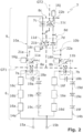
- Fig. 2 shows a schematic circuit diagram of the signal transmission device 3.
- the signal transmission device 3 is designed with the input circuit 6, wherein the input circuit 6 comprises a first input channel 14a and a second input channel 14b .
- the input channels 14a, 14b both run from a first signal input 15a to a second signal input 15b of the signal transmission device 3, to which the poles of the AC signal source 2 are connected (see Fig. 1 ).
- the first input channel 14a is used to receive the first partial signal of the AC signal
- the second input channel 14b is designed to receive the second partial signal of the AC signal.
- the first partial signal of the alternating current signal is a part of the AC signal with a first polarity
- the second partial signal is a part of the AC signal with a second polarity that is opposite to the first polarity.
- the two partial signals follow one another alternately when the AC signal is transmitted and are designed in particular as half-waves.
- the coupling elements 8a, 8b are activated alternately in the sequence of the partial signals of the AC signal in order to feed the respective partial signal of the AC signal from the input circuit 6 into the output circuit 9.
- the signal transmission device 3 has the output circuit 9, wherein the input circuit 6 and the output circuit 9 are galvanically isolated, which is indicated by the dashed line GT1.
- the first input channel 14a has three series-connected electrical resistors 16a, 16b, 16c in the direction from the first signal input 15a to the second signal input 15b to avoid short circuits and for voltage regulation, wherein at least two of the resistors 16a, 16b, 16c of the first input channel 14a differ in at least one characteristic value, especially in their service life.
- the different parameters prevent several or all resistors 16a, 16b, 16c from failing at the same time, which can lead to damage to the signal transmission device 3 and distortion of the AC signal to be transmitted due to the change in the current flow through the first input channel 14a.
- the three resistors 16a, 16b, 16c are followed by the transmitting part 7a of the first coupling element 8a, which is connected in series with the resistors 16a, 16b, 16c, here in the form of a first optocoupler, the transmitting part 7a being designed here as a light-emitting diode or laser diode and the associated receiving part 11a of the first optocoupler 8a being designed here in the form of a phototransistor.
- the receiving part 11a is part of the first output channel 10a of the output circuit 9. In the embodiment shown, the receiving part 11a of the first optocoupler 8a is at a reference potential (here: ground).
- a first collector voltage is applied to a resistor 16g on the receiving part 11a of the first optocoupler 8a.
- the first optocoupler 8a enables transmission of the first partial signal of the AC signal into the first output channel 10a, whereby the first input channel 14a and the first output channel 10a are galvanically isolated from one another.
- a protective diode 18a is connected in parallel to the transmitting part 7a of the first optocoupler 8a.
- voltage direction-dependent electronic switching devices 19a, 19b, 19c are connected in series in the first input channel 14a in the direction from the first signal input 15a to the second signal input 15b after the transmitting part 7a of the first optocoupler 8a.
- These voltage direction-dependent electronic switching devices 19a, 19b, 19c are designed as rectifier diodes, with at least two of the rectifier diodes 19a, 19b, 19c differing in at least one characteristic, in particular in their service life.
- the rectifier diodes 19a, 19b, 19c are aligned with their forward direction towards the second signal input 15b and ensure that only the first partial signal of the AC signal flows through the first input channel 14a, but the second partial signal of the AC signal is blocked.
- the first input channel 14a is therefore only available in one of the two polarities the AC signal source 2 (see Fig. 1 ) is activated.
- the different characteristics of the rectifier diodes 19a, 19b, 19c prevent the rectifier diodes 19a, 19b, 19c from failing at the same time. In particular, it prevents current from flowing through the first input channel 14a with both polarities of the AC signal source 2 and the AC signal to be transmitted from being distorted.
- the second input channel 14b has, corresponding to the first input channel 14a, three series-connected resistors 16d, 16e, 16f in the direction from the second signal input 15b to the first signal input 15a, which are followed by the transmitting part 7b of the second coupling element 8b in the form of a second optocoupler 8b .
- the second optocoupler 8b serves to couple the second partial signal, the polarity of which is opposite to the first partial signal of the AC signal, into the second output channel 10b of the output circuit 9 via the receiving part 11b of the second optocoupler 8b.
- the receiving part 11b of the second optocoupler 8b is at a reference potential (here: ground), whereby the reference potential of the receiving part 11b of the second optocoupler 8b can differ from the reference potential of the receiving part 11a of the first optocoupler 8a.
- a second collector voltage is applied to the resistor 16h on the receiving part 11b of the second optocoupler 8b, which can in particular be identical to the first collector voltage.
- the second partial signal is coupled in by the second optocoupler 8b with galvanic isolation of the second input channel 14b from the second output channel 10b.
- the transmitting part 7b of the second optocoupler 8b is protected against overvoltages by a second protective diode 18b connected in parallel.
- the transmitting part 7b of the second optocoupler 8b is connected in the direction from the second signal input 15b to the first signal input 15a by three series-connected voltage-direction-dependent electronic switching devices 19d, 19e, 19f in the form of rectifier diodes, which are aligned with the forward direction towards the first signal input 15a.
- the rectifier diodes 19a, 19b, 19c of the first input channel 14a on the one hand and the rectifier diodes 19d, 19e, 19f of the second input channel 14b on the other hand are connected with opposite polarity to the AC signal source 2 (see Fig. 1 ) electrically connected.
- the AC signal source 2 see Fig. 1
- At least two of the resistors 16d, 16e, 16f of the second input channel 14b differ in at least one characteristic, in particular the service life.
- at least two of the rectifier diodes 19d, 19e, 19f of the second input channel 14b differ in at least one characteristic. This prevents the resistors 16d, 16e, 16f or the rectifier diodes 19d, 19e, 19f from failing at the same time, which would distort the AC signal to be transmitted.
- each electrical resistor 16a, 16b, 16c of the first input channel 14a match the characteristics of each electrical resistor 16d, 16e, 16f of the second input channel 14b.
- the characteristics of each voltage-direction-dependent electronic switching device 19a, 19b, 19c, here in the form of the rectifier diodes 19a, 19b, 19c, of the first input channel 14a match the characteristics of each voltage-direction-dependent electronic switching device 19d, 19e, 19f of the second input channel 14b.
- the characteristics of the first and second optocouplers 8a, 8b also preferably match.
- the transmitting part 7a of the first optocoupler 8a emits a light signal whose course follows the first partial signal of the AC signal.
- the receiving part 11a of the first optocoupler 8a converts the light signal emitted by the transmitting part 7a of the first optocoupler 8a back into a voltage whose course represents the first partial signal of the AC signal.
- the voltage generated in the transmitting part 7a of the first optocoupler 8a can be tapped from the outside at a first output 21a of the first output channel 10a in order to transmit the first partial signal of the AC signal to an external system, in particular to a processing unit.
- the transmitting part 7b of the second optocoupler 8b emits a light signal whose course follows the second partial signal of the AC signal.
- the receiving part 11b of the second optocoupler 8b converts the light signal emitted by the transmitting part 7b of the second optocoupler 8b back into a voltage whose course represents the second partial signal of the AC signal.
- the voltage generated in the transmitting part 7b of the second optocoupler 8b can be tapped from the outside at a first output 22a of the second output channel 10b in order to transmit the second partial signal of the AC signal to an external system.
- the two partial signals of the AC signal transmitted in this way can be reassembled into an overall signal after transmission or compared with each other with regard to errors during transmission (in particular due to defective components of the signal transmission device 3).
- a transmitting part 7c of a third coupling element 8c in the form of a third optocoupler 8c is arranged in the first output channel 10a, which emits a light signal whose course follows the voltage that is present at the receiving part 11a of the first optocoupler 8a.
- This signal is received by a receiving part 11c of the third optocoupler 8c, which is arranged in the second output channel 10b. Since the voltage at the receiving part 11a of the first optocoupler 8a follows the first partial signal of the AC signal, the signal transmitted by the third optocoupler 8c represents the first partial signal of the AC signal.
- a transmitting part 7d of a fourth coupling element 8d in the form of a fourth optocoupler 8d is arranged, wherein the transmitting part 7d emits a light signal, the course of which follows the voltage applied to the receiving part 11b of the second optocoupler 8b.
- This signal is received by a receiving part 11d of the fourth optocoupler 8d, wherein the receiving part 11d is arranged in the first output channel 10a. Since the voltage at the receiving part 11b of the second optocoupler 8b follows the second partial signal of the AC signal, the signal transmitted by the fourth optocoupler 8d represents the second partial signal of the AC signal.
- the second partial signal of the AC signal is thus also transmitted to the first output channel 10a and can be tapped there at a second output 21b of the first output channel 10a.
- the first collector voltage is preferably present at a resistor 16i on the fourth optocoupler 8d.
- the partial signals tapped at the outputs 21a, 21b of the first output channel 10a can be compared with one another by means of an evaluation unit (not shown).
- the partial signals tapped at the outputs 22a, 22b of the second output channel 10b can be compared with one another by means of the evaluation unit.
- the first output channel 10a and the second output channel 10b are grounded between the receiving parts 11c, 11d and the transmitting parts 7c, 7d of the third and fourth optocouplers 8c, 8d so that the signals transmitted in the third and fourth optocouplers 8c, 8d do not influence each other.
- the coupling of the first and second partial signals from one output channel 10a, 10b into the other output channel 10a, 10b is carried out by the third and fourth optocouplers 8c, 8d with galvanic isolation of the output channels 10a, 10b (shown by the dashed line GT2 ) in order to avoid interference potentials between the output channels 10a, 10b.
Landscapes
- Engineering & Computer Science (AREA)
- Mechanical Engineering (AREA)
- Automation & Control Theory (AREA)
- Train Traffic Observation, Control, And Security (AREA)
- Transmitters (AREA)
- Dc Digital Transmission (AREA)
Claims (11)
- Dispositif de transmission de signal (3) d'une installation de sécurité de signalisation (1) permettant la transmission sûre d'une information de signal d'un signal AC à une unité de traitement (4), présentant :• un circuit d'entrée (6) permettant la détection du signal AC, dans lequel le circuit d'entrée (6) comprend un premier canal d'entrée (14a) et un second canal d'entrée (14b),• un circuit de sortie (9) permettant l'évaluation du signal AC, dans lequel le circuit de sortie (9) comprend au moins un premier canal de sortie (10a) et au moins un second canal de sortie (10b), dans lequel le premier canal de sortie (10a) et le second canal de sortie (10b) sont séparés galvaniquement l'un de l'autre,dans lequel le premier canal d'entrée (14a) est relié à l'au moins un premier canal de sortie (10a) par l'intermédiaire d'un premier élément de couplage (8a), mais est séparé galvaniquement de l'au moins un premier canal de sortie (10a),dans lequel le second canal d'entrée (14b) est relié à l'au moins un second canal de sortie (10b) par l'intermédiaire d'un second élément de couplage (8b), mais est séparé galvaniquement de l'au moins un second canal de sortie (10b),dans lequel chaque canal d'entrée (14a, 14b) comprend plusieurs résistances (16a - 16f) connectées en série,caractérisé en cequ'au moins deux des résistances (16a - 16f) de chaque canal d'entrée (14a, 14b) se différencient par au moins une grandeur caractéristique, etque chaque canal d'entrée (14a, 14b) comprend plusieurs dispositifs de commutation électroniques (19a - 19f) dépendant du sens de la tension, connectés en série, dans lequel au moins deux des dispositifs de commutation électroniques (19a - 19f) dépendant du sens de la tension de chaque canal d'entrée (14a, 14b) se différencient par au moins une grandeur caractéristique, et dans lequel les dispositifs de commutation électroniques (19a - 19c) dépendant du sens de la tension du premier canal d'entrée (14a) sont reliés électriquement à la source de signal AC (2) avec une polarité opposée à celle des dispositifs de commutation électroniques (19d - 19f) dépendant du sens de la tension du second canal d'entrée (14b).
- Dispositif de transmission de signal selon la revendication 1,
caractérisé en ce qu'au moins l'une des résistances (16a - 16f), de préférence toutes les résistances (16a - 16f), présentent une construction qui permet un court-circuit en cas de défaut. - Dispositif de transmission de signal selon l'une des revendications précédentes, caractérisé en ce que l'au moins une grandeur caractéristique est le fabricant et/ou la durée de vie et/ou la robustesse et/ou des valeurs nominales et/ou des formes de composants et/ou des technologies de composants.
- Dispositif de transmission de signal selon l'une des revendications précédentes, caractérisé en ce que les éléments de couplage (8a, 8b) sont des optocoupleurs.
- Dispositif de transmission de signal selon l'une des revendications précédentes, caractérisé en ce que le circuit de sortie (9) est conçu pour transmettre des informations de signal du premier canal de sortie (10a) au second canal de sortie (10b) et du second canal de sortie (10b) au premier canal de sortie (10a) à l'aide d'autres éléments de couplage (8c, 8d).
- Dispositif de transmission de signal selon la revendication 5,
caractérisé en ce qu'un troisième optocoupleur (8c) est utilisé pour la transmission des informations de signal du premier canal de sortie (10a) au second canal de sortie (10b) et un quatrième optocoupleur (8d) est utilisé pour la transmission des informations de signal du second canal de sortie (10b) au premier canal de sortie (10a), dans lequel le premier canal de sortie (10a) comprend la partie d'émission (7c) du troisième optocoupleur (8c) et la partie de réception (11d) du quatrième optocoupleur (8d), et dans lequel le second canal de sortie (10b) comprend la partie d'émission (7d) du quatrième optocoupleur (8d) et la partie de réception (11c) du troisième optocoupleur (8c). - Dispositif de transmission de signal selon la revendication 5 ou 6, caractérisé en ce que les canaux de sortie (10a, 10b) sont conçus pour comparer l'information de signal du premier canal de sortie (10a) à l'information de signal du second canal de sortie (10b).
- Dispositif de transmission de signal selon l'une des revendications précédentes, caractérisé en ce que le dispositif de transmission de signal (3) fait partie d'un poste d'aiguillage, d'un appareil de véhicule, d'un élément de champ, en particulier d'un compteur d'essieux, ou d'un élément de commande.
- Installation de sécurité de signalisation (1) comportant une unité de traitement (4), une source de signal AC (2) pour la fourniture d'un signal AC, et un dispositif de transmission de signal (3) selon l'une des revendications précédentes.
- Installation de sécurité de signalisation selon la revendication 9, caractérisée en ce que la source de signal AC (2) est un élément de champ, en particulier un signal de trafic, et en ce que le signal AC indique l'état de commutation de l'élément de champ.
- Utilisation d'un dispositif de transmission de signal (3) selon l'une des revendications 1 à 8 pour la révélation de défauts dans un système critique pour la sécurité.
Priority Applications (7)
| Application Number | Priority Date | Filing Date | Title |
|---|---|---|---|
| PL22188972.8T PL4316945T3 (pl) | 2022-08-05 | 2022-08-05 | Urządzenie do przesyłania sygnałów w sygnałowej instalacji bezpieczeństwa, służące do bezpiecznego przesyłania sygnału zmiennoprądowego |
| HUE22188972A HUE071483T2 (hu) | 2022-08-05 | 2022-08-05 | Jelátviteli berendezés jelzéstechnikai biztosítóberendezésben egy AC jel biztonságos átviteléhez |
| DK22188972.8T DK4316945T3 (da) | 2022-08-05 | 2022-08-05 | Signaloverførselsindretning i et signalteknisk sikkerhedsanlæg til sikker overførsel af et vekselstrømssignal |
| FIEP22188972.8T FI4316945T3 (fi) | 2022-08-05 | 2022-08-05 | Signaaliturvajärjestelmän signaalinlähetyslaite ac-signaalin suojattua lähettämistä varten |
| ES22188972T ES3028087T3 (en) | 2022-08-05 | 2022-08-05 | Signal transmission device of a signal securing system for securely transmitting an ac signal |
| PT221889728T PT4316945T (pt) | 2022-08-05 | 2022-08-05 | Dispositivo de transmissão de sinais de um sistema de proteção de sinais para a transmissão segura de um sinal de corrente alternada |
| EP22188972.8A EP4316945B1 (fr) | 2022-08-05 | 2022-08-05 | Dispositif de transmission de signal d'une installation technique de sécurité de signal destiné à la transmission sécurisée d'un signal de courant alternatif |
Applications Claiming Priority (1)
| Application Number | Priority Date | Filing Date | Title |
|---|---|---|---|
| EP22188972.8A EP4316945B1 (fr) | 2022-08-05 | 2022-08-05 | Dispositif de transmission de signal d'une installation technique de sécurité de signal destiné à la transmission sécurisée d'un signal de courant alternatif |
Publications (2)
| Publication Number | Publication Date |
|---|---|
| EP4316945A1 EP4316945A1 (fr) | 2024-02-07 |
| EP4316945B1 true EP4316945B1 (fr) | 2025-01-22 |
Family
ID=83232726
Family Applications (1)
| Application Number | Title | Priority Date | Filing Date |
|---|---|---|---|
| EP22188972.8A Active EP4316945B1 (fr) | 2022-08-05 | 2022-08-05 | Dispositif de transmission de signal d'une installation technique de sécurité de signal destiné à la transmission sécurisée d'un signal de courant alternatif |
Country Status (7)
| Country | Link |
|---|---|
| EP (1) | EP4316945B1 (fr) |
| DK (1) | DK4316945T3 (fr) |
| ES (1) | ES3028087T3 (fr) |
| FI (1) | FI4316945T3 (fr) |
| HU (1) | HUE071483T2 (fr) |
| PL (1) | PL4316945T3 (fr) |
| PT (1) | PT4316945T (fr) |
Family Cites Families (4)
| Publication number | Priority date | Publication date | Assignee | Title |
|---|---|---|---|---|
| DE3338490A1 (de) * | 1983-10-22 | 1985-05-02 | Standard Elektrik Lorenz Ag, 7000 Stuttgart | Schaltungsanordnung zur ueberwachung des betriebszustandes von in der aussenanlage eines stellwerks eingesetzten wechselstromverbrauchern |
| DE102007004917B4 (de) * | 2007-01-26 | 2010-09-30 | Siemens Ag | Verfahren und Anordnung zur Ansteuerung und Überwachung von Feldelementen |
| CN105759204B (zh) | 2016-04-15 | 2018-11-30 | 上汽通用汽车有限公司 | 车用交流充电装置的诊断电路及诊断方法 |
| WO2020210321A1 (fr) * | 2019-04-08 | 2020-10-15 | Metrom Rail, Llc. | Procédés et systèmes pour accomplir une commande vitale de train à base de bande ultralarge (uwb) |
-
2022
- 2022-08-05 ES ES22188972T patent/ES3028087T3/es active Active
- 2022-08-05 PT PT221889728T patent/PT4316945T/pt unknown
- 2022-08-05 EP EP22188972.8A patent/EP4316945B1/fr active Active
- 2022-08-05 DK DK22188972.8T patent/DK4316945T3/da active
- 2022-08-05 FI FIEP22188972.8T patent/FI4316945T3/fi active
- 2022-08-05 HU HUE22188972A patent/HUE071483T2/hu unknown
- 2022-08-05 PL PL22188972.8T patent/PL4316945T3/pl unknown
Also Published As
| Publication number | Publication date |
|---|---|
| FI4316945T3 (fi) | 2025-04-09 |
| PL4316945T3 (pl) | 2025-08-11 |
| PT4316945T (pt) | 2025-04-04 |
| HUE071483T2 (hu) | 2025-08-28 |
| ES3028087T3 (en) | 2025-06-18 |
| DK4316945T3 (da) | 2025-04-07 |
| EP4316945A1 (fr) | 2024-02-07 |
Similar Documents
| Publication | Publication Date | Title |
|---|---|---|
| EP2980659B1 (fr) | Dispositif et procédé destinés à la surveillance et la commutation d'un circuit de charge | |
| EP2906441B1 (fr) | Ensemble de circuit de décharge d'un accumulateur d'énergie électrique et convertisseur statique équipé d'un tel ensemble de circuit | |
| EP3014365B1 (fr) | Dispositif de commutation de sécurité pour détecter des entrées non conformes | |
| DE4441070C2 (de) | Sicherheitsschalteranordnung | |
| EP2956366B1 (fr) | Surveillance de circuit de sécurité avec tension alternative | |
| EP2720094A1 (fr) | Système de sécurité | |
| EP2378663B1 (fr) | Circuit d'entrée sécurisé doté d'un raccordement périphérique sur un canal unique pour l'entrée d'un utilisateur de bus | |
| DE102014019725C5 (de) | Elektronische Schaltvorrichtung und elektronisches Schaltverfahren | |
| WO2007112942A1 (fr) | Dispositif de commutation et de contrôle d'un système de signaux lumineux pour trafic ferroviaire | |
| EP3745596B1 (fr) | Circuit d'entrée numérique permettant de recevoir des signaux d'entrée numérique d'au moins un émetteur de signaux | |
| EP0172454B1 (fr) | Dispositif de contrôle pour installations de feux de signalisation | |
| EP0660043B1 (fr) | Dispositif de commande pour commander des appareils de commutation selon un programme de temps | |
| EP4316945A1 (fr) | Dispositif de transmission de signal d'une installation technique de sécurité de signal destiné à la transmission sécurisée d'un signal ca | |
| EP0809361B1 (fr) | Dispositif électronique de commutation et circuit pour la surveillance d'une installation technique | |
| EP1034553A1 (fr) | Circuit de surveillance d'un commutateur a courant alternatif | |
| DE102020112985A1 (de) | IO-Link-Adapter | |
| DE3519252A1 (de) | Fehlersichere logikschaltung | |
| DE19620065C2 (de) | Schaltungsanordnung zur Überwachung des fehlerfreien und/oder zur Erkennung eines fehlerbehafteten Zustands einer Anlage | |
| DE102010045990B4 (de) | Verfahren zum Betreiben eines Kraftwagens | |
| EP3281365B1 (fr) | Dispositif d'extension d'interface pour un dispositif réseau et procédé de fonctionnement d'un dispositif d'extension d'interface | |
| EP1068700B1 (fr) | Etage de sortie de signalisation servant a produire des signaux de tension numeriques sur un systeme de bus | |
| EP0596584B1 (fr) | Arrangement de saisie de perturbation | |
| DE102016119496A1 (de) | System zur Erfassung eines Sicherungszustands | |
| DE102014116188A1 (de) | System zum fehlersicheren Abschalten eines elektrischen Verbrauchers | |
| EP0763877A2 (fr) | Systéme de communication |
Legal Events
| Date | Code | Title | Description |
|---|---|---|---|
| PUAI | Public reference made under article 153(3) epc to a published international application that has entered the european phase |
Free format text: ORIGINAL CODE: 0009012 |
|
| STAA | Information on the status of an ep patent application or granted ep patent |
Free format text: STATUS: THE APPLICATION HAS BEEN PUBLISHED |
|
| AK | Designated contracting states |
Kind code of ref document: A1 Designated state(s): AL AT BE BG CH CY CZ DE DK EE ES FI FR GB GR HR HU IE IS IT LI LT LU LV MC MK MT NL NO PL PT RO RS SE SI SK SM TR |
|
| STAA | Information on the status of an ep patent application or granted ep patent |
Free format text: STATUS: REQUEST FOR EXAMINATION WAS MADE |
|
| 17P | Request for examination filed |
Effective date: 20240410 |
|
| RBV | Designated contracting states (corrected) |
Designated state(s): AL AT BE BG CH CY CZ DE DK EE ES FI FR GB GR HR HU IE IS IT LI LT LU LV MC MK MT NL NO PL PT RO RS SE SI SK SM TR |
|
| P01 | Opt-out of the competence of the unified patent court (upc) registered |
Free format text: CASE NUMBER: APP_35463/2024 Effective date: 20240613 |
|
| GRAP | Despatch of communication of intention to grant a patent |
Free format text: ORIGINAL CODE: EPIDOSNIGR1 |
|
| STAA | Information on the status of an ep patent application or granted ep patent |
Free format text: STATUS: GRANT OF PATENT IS INTENDED |
|
| RIC1 | Information provided on ipc code assigned before grant |
Ipc: B61L 27/70 20220101ALI20240731BHEP Ipc: B61L 5/18 20060101ALI20240731BHEP Ipc: B61L 1/16 20060101AFI20240731BHEP |
|
| INTG | Intention to grant announced |
Effective date: 20240813 |
|
| RAP3 | Party data changed (applicant data changed or rights of an application transferred) |
Owner name: HITACHI RAIL GTS DEUTSCHLAND GMBH |
|
| GRAS | Grant fee paid |
Free format text: ORIGINAL CODE: EPIDOSNIGR3 |
|
| GRAA | (expected) grant |
Free format text: ORIGINAL CODE: 0009210 |
|
| STAA | Information on the status of an ep patent application or granted ep patent |
Free format text: STATUS: THE PATENT HAS BEEN GRANTED |
|
| AK | Designated contracting states |
Kind code of ref document: B1 Designated state(s): AL AT BE BG CH CY CZ DE DK EE ES FI FR GB GR HR HU IE IS IT LI LT LU LV MC MK MT NL NO PL PT RO RS SE SI SK SM TR |
|
| REG | Reference to a national code |
Ref country code: GB Ref legal event code: FG4D Free format text: NOT ENGLISH |
|
| REG | Reference to a national code |
Ref country code: CH Ref legal event code: EP |
|
| REG | Reference to a national code |
Ref country code: IE Ref legal event code: FG4D Free format text: LANGUAGE OF EP DOCUMENT: GERMAN |
|
| REG | Reference to a national code |
Ref country code: DE Ref legal event code: R096 Ref document number: 502022002698 Country of ref document: DE |
|
| REG | Reference to a national code |
Ref country code: PT Ref legal event code: SC4A Ref document number: 4316945 Country of ref document: PT Date of ref document: 20250404 Kind code of ref document: T Free format text: AVAILABILITY OF NATIONAL TRANSLATION Effective date: 20250331 |
|
| REG | Reference to a national code |
Ref country code: DK Ref legal event code: T3 Effective date: 20250403 |
|
| REG | Reference to a national code |
Ref country code: FI Ref legal event code: FGE |
|
| REG | Reference to a national code |
Ref country code: NL Ref legal event code: FP |
|
| REG | Reference to a national code |
Ref country code: SE Ref legal event code: TRGR |
|
| REG | Reference to a national code |
Ref country code: ES Ref legal event code: FG2A Ref document number: 3028087 Country of ref document: ES Kind code of ref document: T3 Effective date: 20250618 |
|
| PG25 | Lapsed in a contracting state [announced via postgrant information from national office to epo] |
Ref country code: RS Free format text: LAPSE BECAUSE OF FAILURE TO SUBMIT A TRANSLATION OF THE DESCRIPTION OR TO PAY THE FEE WITHIN THE PRESCRIBED TIME-LIMIT Effective date: 20250422 |
|
| REG | Reference to a national code |
Ref country code: LT Ref legal event code: MG9D |
|
| PG25 | Lapsed in a contracting state [announced via postgrant information from national office to epo] |
Ref country code: IS Free format text: LAPSE BECAUSE OF FAILURE TO SUBMIT A TRANSLATION OF THE DESCRIPTION OR TO PAY THE FEE WITHIN THE PRESCRIBED TIME-LIMIT Effective date: 20250522 |
|
| PG25 | Lapsed in a contracting state [announced via postgrant information from national office to epo] |
Ref country code: HR Free format text: LAPSE BECAUSE OF FAILURE TO SUBMIT A TRANSLATION OF THE DESCRIPTION OR TO PAY THE FEE WITHIN THE PRESCRIBED TIME-LIMIT Effective date: 20250122 |
|
| REG | Reference to a national code |
Ref country code: SK Ref legal event code: T3 Ref document number: E 46445 Country of ref document: SK |
|
| PG25 | Lapsed in a contracting state [announced via postgrant information from national office to epo] |
Ref country code: LV Free format text: LAPSE BECAUSE OF FAILURE TO SUBMIT A TRANSLATION OF THE DESCRIPTION OR TO PAY THE FEE WITHIN THE PRESCRIBED TIME-LIMIT Effective date: 20250122 |
|
| PG25 | Lapsed in a contracting state [announced via postgrant information from national office to epo] |
Ref country code: BG Free format text: LAPSE BECAUSE OF FAILURE TO SUBMIT A TRANSLATION OF THE DESCRIPTION OR TO PAY THE FEE WITHIN THE PRESCRIBED TIME-LIMIT Effective date: 20250122 Ref country code: GR Free format text: LAPSE BECAUSE OF FAILURE TO SUBMIT A TRANSLATION OF THE DESCRIPTION OR TO PAY THE FEE WITHIN THE PRESCRIBED TIME-LIMIT Effective date: 20250423 |
|
| PGFP | Annual fee paid to national office [announced via postgrant information from national office to epo] |
Ref country code: LU Payment date: 20250725 Year of fee payment: 4 |
|
| REG | Reference to a national code |
Ref country code: HU Ref legal event code: AG4A Ref document number: E071483 Country of ref document: HU |
|
| PGFP | Annual fee paid to national office [announced via postgrant information from national office to epo] |
Ref country code: NL Payment date: 20250814 Year of fee payment: 4 |
|
| PGFP | Annual fee paid to national office [announced via postgrant information from national office to epo] |
Ref country code: HU Payment date: 20250813 Year of fee payment: 4 |
|
| PG25 | Lapsed in a contracting state [announced via postgrant information from national office to epo] |
Ref country code: SM Free format text: LAPSE BECAUSE OF FAILURE TO SUBMIT A TRANSLATION OF THE DESCRIPTION OR TO PAY THE FEE WITHIN THE PRESCRIBED TIME-LIMIT Effective date: 20250122 |
|
| PGFP | Annual fee paid to national office [announced via postgrant information from national office to epo] |
Ref country code: PT Payment date: 20250718 Year of fee payment: 4 Ref country code: FI Payment date: 20250814 Year of fee payment: 4 Ref country code: ES Payment date: 20250905 Year of fee payment: 4 |
|
| PGFP | Annual fee paid to national office [announced via postgrant information from national office to epo] |
Ref country code: DE Payment date: 20250730 Year of fee payment: 4 Ref country code: DK Payment date: 20250814 Year of fee payment: 4 |
|
| PGFP | Annual fee paid to national office [announced via postgrant information from national office to epo] |
Ref country code: NO Payment date: 20250808 Year of fee payment: 4 |
|
| PGFP | Annual fee paid to national office [announced via postgrant information from national office to epo] |
Ref country code: PL Payment date: 20250729 Year of fee payment: 4 Ref country code: IT Payment date: 20250901 Year of fee payment: 4 Ref country code: TR Payment date: 20250729 Year of fee payment: 4 |
|
| PGFP | Annual fee paid to national office [announced via postgrant information from national office to epo] |
Ref country code: BE Payment date: 20250818 Year of fee payment: 4 |
|
| PGFP | Annual fee paid to national office [announced via postgrant information from national office to epo] |
Ref country code: FR Payment date: 20250808 Year of fee payment: 4 Ref country code: AT Payment date: 20251020 Year of fee payment: 4 |
|
| PGFP | Annual fee paid to national office [announced via postgrant information from national office to epo] |
Ref country code: SE Payment date: 20250728 Year of fee payment: 4 Ref country code: CH Payment date: 20250901 Year of fee payment: 4 |
|
| PG25 | Lapsed in a contracting state [announced via postgrant information from national office to epo] |
Ref country code: EE Free format text: LAPSE BECAUSE OF FAILURE TO SUBMIT A TRANSLATION OF THE DESCRIPTION OR TO PAY THE FEE WITHIN THE PRESCRIBED TIME-LIMIT Effective date: 20250122 |
|
| PGFP | Annual fee paid to national office [announced via postgrant information from national office to epo] |
Ref country code: CZ Payment date: 20250729 Year of fee payment: 4 |
|
| REG | Reference to a national code |
Ref country code: DE Ref legal event code: R097 Ref document number: 502022002698 Country of ref document: DE |
|
| PGFP | Annual fee paid to national office [announced via postgrant information from national office to epo] |
Ref country code: RO Payment date: 20250728 Year of fee payment: 4 |
|
| PGFP | Annual fee paid to national office [announced via postgrant information from national office to epo] |
Ref country code: SK Payment date: 20250723 Year of fee payment: 4 |
|
| PLBE | No opposition filed within time limit |
Free format text: ORIGINAL CODE: 0009261 |
|
| STAA | Information on the status of an ep patent application or granted ep patent |
Free format text: STATUS: NO OPPOSITION FILED WITHIN TIME LIMIT |
|
| 26N | No opposition filed |
Effective date: 20251023 |
|
| PG25 | Lapsed in a contracting state [announced via postgrant information from national office to epo] |
Ref country code: MC Free format text: LAPSE BECAUSE OF FAILURE TO SUBMIT A TRANSLATION OF THE DESCRIPTION OR TO PAY THE FEE WITHIN THE PRESCRIBED TIME-LIMIT Effective date: 20250122 |