EP4317545A1 - Einkristalliner diamant und herstellungsverfahren dafür - Google Patents
Einkristalliner diamant und herstellungsverfahren dafür Download PDFInfo
- Publication number
- EP4317545A1 EP4317545A1 EP22781144.5A EP22781144A EP4317545A1 EP 4317545 A1 EP4317545 A1 EP 4317545A1 EP 22781144 A EP22781144 A EP 22781144A EP 4317545 A1 EP4317545 A1 EP 4317545A1
- Authority
- EP
- European Patent Office
- Prior art keywords
- crystal diamond
- less
- crystal
- diamond
- sample
- Prior art date
- Legal status (The legal status is an assumption and is not a legal conclusion. Google has not performed a legal analysis and makes no representation as to the accuracy of the status listed.)
- Pending
Links
Images

Classifications
-
- C—CHEMISTRY; METALLURGY
- C30—CRYSTAL GROWTH
- C30B—SINGLE-CRYSTAL GROWTH; UNIDIRECTIONAL SOLIDIFICATION OF EUTECTIC MATERIAL OR UNIDIRECTIONAL DEMIXING OF EUTECTOID MATERIAL; REFINING BY ZONE-MELTING OF MATERIAL; PRODUCTION OF A HOMOGENEOUS POLYCRYSTALLINE MATERIAL WITH DEFINED STRUCTURE; SINGLE CRYSTALS OR HOMOGENEOUS POLYCRYSTALLINE MATERIAL WITH DEFINED STRUCTURE; AFTER-TREATMENT OF SINGLE CRYSTALS OR A HOMOGENEOUS POLYCRYSTALLINE MATERIAL WITH DEFINED STRUCTURE; APPARATUS THEREFOR
- C30B29/00—Single crystals or homogeneous polycrystalline material with defined structure characterised by the material or by their shape
- C30B29/02—Elements
- C30B29/04—Diamond
-
- B—PERFORMING OPERATIONS; TRANSPORTING
- B01—PHYSICAL OR CHEMICAL PROCESSES OR APPARATUS IN GENERAL
- B01J—CHEMICAL OR PHYSICAL PROCESSES, e.g. CATALYSIS OR COLLOID CHEMISTRY; THEIR RELEVANT APPARATUS
- B01J3/00—Processes of utilising sub-atmospheric or super-atmospheric pressure to effect chemical or physical change of matter; Apparatus therefor
- B01J3/06—Processes using ultra-high pressure, e.g. for the formation of diamonds; Apparatus therefor, e.g. moulds or dies
-
- C—CHEMISTRY; METALLURGY
- C01—INORGANIC CHEMISTRY
- C01B—NON-METALLIC ELEMENTS; COMPOUNDS THEREOF; METALLOIDS OR COMPOUNDS THEREOF NOT COVERED BY SUBCLASS C01C
- C01B32/00—Carbon; Compounds thereof
- C01B32/25—Diamond
-
- C—CHEMISTRY; METALLURGY
- C01—INORGANIC CHEMISTRY
- C01B—NON-METALLIC ELEMENTS; COMPOUNDS THEREOF; METALLOIDS OR COMPOUNDS THEREOF NOT COVERED BY SUBCLASS C01C
- C01B32/00—Carbon; Compounds thereof
- C01B32/25—Diamond
- C01B32/26—Preparation
-
- C—CHEMISTRY; METALLURGY
- C30—CRYSTAL GROWTH
- C30B—SINGLE-CRYSTAL GROWTH; UNIDIRECTIONAL SOLIDIFICATION OF EUTECTIC MATERIAL OR UNIDIRECTIONAL DEMIXING OF EUTECTOID MATERIAL; REFINING BY ZONE-MELTING OF MATERIAL; PRODUCTION OF A HOMOGENEOUS POLYCRYSTALLINE MATERIAL WITH DEFINED STRUCTURE; SINGLE CRYSTALS OR HOMOGENEOUS POLYCRYSTALLINE MATERIAL WITH DEFINED STRUCTURE; AFTER-TREATMENT OF SINGLE CRYSTALS OR A HOMOGENEOUS POLYCRYSTALLINE MATERIAL WITH DEFINED STRUCTURE; APPARATUS THEREFOR
- C30B19/00—Liquid-phase epitaxial-layer growth
Definitions
- the present disclosure relates to a single-crystal diamond and a method of manufacturing the single-crystal diamond.
- the present application claims priority to Japanese Patent Application No. 2021-061207, filed March 31, 2021 . The entire contents of this Japanese patent application are incorporated herein by reference.
- Diamonds have been used in various applications, such as heat sinks, wire-drawing dies, precision machining tools, optical components, laser windows, crystals for spectroscopy, monochromators, anvils for ultra-high pressure generators, and semiconductor diamond substrates.
- applications in particular, in the fields of optical components, laser windows, crystals for spectroscopy, monochromators, anvils for ultra-high pressure generators, and semiconductor diamond substrates, diamonds with fewer crystal defects and less distortion have been developed to improve performance (for example, Patent Literature 1 to Patent Literature 3).
- the present disclosure provides a single-crystal diamond having an X-ray diffraction rocking curve with a half-width of 20 seconds or less,
- the present disclosure provides a method of manufacturing the single-crystal diamond, the method including:
- substitutional nitrogen is added to a diamond.
- To add an appropriate amount of impurity it is necessary to devise the addition of a specific element to a solvent metal or a raw material for single-crystal diamond synthesis, or the like.
- Such a contrivance causes a specific element raw material to be incorporated into a crystal and induces a crystal defect. Furthermore, contamination with impurities itself caused fluctuations in contamination with impurities during growth and caused a difference in the manner of incorporating impurities between growth sectors. This caused a subtle difference in lattice spacing and caused distortion.
- the present disclosure can provide a single-crystal diamond with fewer crystal defects and less distortion even to which nitrogen is added in a controlled manner.
- a to B refers to the upper and lower limits of the range (that is, A or more and B or less).
- the unit of A and the unit of B are the same.
- half-width refers to the "full-width at half maximum (FWHM)”.
- () indicates an individual plane, and ⁇ ⁇ indicates a group plane.
- a single-crystal diamond according to an embodiment of the present disclosure (hereinafter also referred to as "the present embodiment")
- a single-crystal diamond having an X-ray diffraction rocking curve with a smaller half-width has higher crystallinity and fewer crystal defects and less distortion.
- the single-crystal diamond according to the present embodiment has an X-ray diffraction rocking curve with a half-width of 20 seconds or less, high crystallinity, and fewer crystal defects and less distortion.
- the upper limit of the half-width of the X-ray diffraction rocking curve of the single-crystal diamond is 20 seconds or less, preferably 10 seconds or less, more preferably 8 seconds or less, still more preferably 6 seconds or less, from the perspective of improving crystallinity.
- the lower limit of the half-width of the X-ray diffraction rocking curve of the single-crystal diamond can be 4.2 seconds or more from the perspective of manufacture.
- the half-width of the X-ray diffraction rocking curve of the single-crystal diamond is preferably 4.2 seconds to 20 seconds, more preferably 4.2 seconds to 10 seconds, still more preferably 4.2 seconds to 8 seconds, still more preferably 4.2 seconds to 6 seconds.
- the half-width of the X-ray diffraction rocking curve of the single-crystal diamond is measured with CuK ⁇ radiation in a (004) plane parallel arrangement using a diamond crystal as a first crystal in X-ray diffraction by a double-crystal method.
- a diamond crystal cut out from the single-crystal diamond to be measured is used as the first crystal and a second crystal.
- the half-width of the rocking curve reflects the crystallinity of both the first crystal and the second crystal.
- the half-width of the rocking curve is a value that sensitively reflects the quality of the crystallinity of the sample.
- a single-crystal diamond has higher crystallinity when a diamond phonon peak appearing at a Raman shift in the range of 1332 cm -1 to 1333 cm -1 in Raman spectroscopy of the single-crystal diamond is sharp and has a smaller half-width.
- the single-crystal diamond according to the present embodiment has a half-width of 2.0 cm -1 or less in a peak at a Raman shift in the range of 1332 cm -1 to 1333 cm -1 in a Raman spectrum (hereinafter also referred to as a "half-width of a peak in a Raman spectrum”) and has high crystallinity.
- the upper limit of the half-width of a peak in a Raman spectrum of a single-crystal diamond is 2.0 cm -1 or less, preferably 1.9 cm -1 or less, more preferably 1.8 cm -1 or less, still more preferably 1.7 cm -1 or less.
- the lower limit of the half-width of a peak in a Raman spectrum of a single-crystal diamond can be 1.6 cm -1 or more from the perspective of manufacture.
- the half-width of a peak in a Raman spectrum of a single-crystal diamond preferably ranges from 1.6 cm -1 to 2.0 cm -1 , more preferably 1.6 cm -1 to 1.9 cm -1 , still more preferably 1.6 cm -1 to 1.8 cm -1 , still more preferably 1.6 cm -1 to 1.7 cm -1 .
- the half-width of a peak in a Raman spectrum is measured by the following procedure.
- a surface of a measurement sample that is, a single-crystal diamond is polished with a metal bonded grinding wheel to a surface roughness Ra of 20 nm or less.
- the measurement sample is typically and preferably close to square or octagonal.
- the polished surface is irradiated with a laser under the following conditions, and scattered Raman lines are detected.
- a spectrum analysis is performed on the Raman lines detected at the five positions to identify a diamond phonon peak appearing at a Raman shift in the range of 1332 cm -1 to 1333 cm -1 .
- the Lorentz function is fitted to the diamond phonon peak by the least squares method to determine the half-width of the peak at each of the five positions at the Raman shift in the range of 1332 cm -1 to 1333 cm -1 .
- the half-width at the central portion and the half-widths at the other four positions are weighted-averaged at a ratio of 4:1.
- the crystallinity, such as distortion, of a sample can be uniquely evaluated and compared among samples by the setting of the measurement regions at the five positions and by the calculation method of the weighted average thereof.
- etch-pit density refers to a measure indicating the number of linear defects derived from a needle-like defect linearly extending in a single-crystal diamond, and is measured in an etching test described later.
- a single-crystal diamond with a smaller etch-pit density has fewer defects and higher crystallinity.
- the single-crystal diamond according to the present embodiment has an etch-pit density of 10,000 /cm 2 or less and high crystallinity.
- the upper limit of the etch-pit density of a single-crystal diamond is 10,000 /cm 2 or less, preferably 1000 /cm 2 or less, more preferably 100 /cm 2 or less, still more preferably 10 /cm 2 or less.
- the lower limit of the etch-pit density of a single-crystal diamond can be 0 /cm 2 or more.
- the etch-pit density of a single-crystal diamond preferably ranges from 0 /cm 2 to 10,000 /cm 2 , more preferably 0 /cm 2 to 1000 /cm 2 , still more preferably 0 /cm 2 to 100 /cm 2 , still more preferably 0 /cm 2 to 10 /cm 2 .
- the etch-pit density of the single-crystal diamond is measured in an etching test. More specifically, it is measured by the following procedure.
- a single-crystal diamond is immersed in a potassium nitrate (KNO 3 ) melt etchant and is heated in a platinum crucible at 600°C to 700°C for 0.5 to 2 hours. After slow cooling, the single-crystal diamond is taken out, and the main growth surface is observed with an optical microscope. An inverted pyramidal etch pit is observed, and the size of the etch pit is adjusted by the crucible temperature and the treatment time depending on the etch-pit density. For this adjustment, first, the etch-pit density is roughly determined by treatment under conditions where a small etch pit can be formed (the crucible temperature and the treatment time), and the measurement conditions (the crucible temperature and the treatment time) are then determined.
- KNO 3 potassium nitrate
- the dimensions (size) of an etch pit are determined for each etch-pit density such that etch pits do not overlap.
- the number of etch pits does not change while the etch pits are enlarged, and the size of etch pits is adjusted to the size of the field of view to be evaluated (the density of etch pits).
- the size of etch pits ranges from approximately 5 to 20 ⁇ m square such that etch pits do not overlap.
- Three regions with a high etch-pit density are selected in a growth surface, and a rectangular measurement region of 1 mm or less is determined in each region.
- the area where 100 etch pits are present is measured in each measurement region, and the number of etch pits per cm 2 is calculated on the basis of the number of etch pits (100) and the area.
- the average of the etch-pit densities in the three measurement regions is referred to as "the etch-pit density of a single-crystal diamond" in the present description.
- etch-pit density is referred to as "the etch-pit density of a single-crystal diamond" in the present description.
- etch pit refers to a clear inverted pyramidal pit. Etch pits of approximately the same size are distributed and can be identified as etch pits. In a sample of 5000 /cm 2 or more, etch pits with a size in the range of 1/4 of the size of the majority of etch pits (the size of d50 on an area basis) to the largest size are counted. In a sample of less than 5000 /cm 2 , etch pits with a size in the range of 1/8 of the size of the majority of etch pits (the size of d50 on an area basis) to the largest size are counted.
- the number of etch pits per cm 2 corresponds to the density of the linear defects.
- the average number of etch pits in the measurement method is referred to as "the density of dislocation defects passing through the main growth surface" in the present embodiment.
- the nitrogen in a single-crystal diamond causes a crystal defect and distortion, and from this perspective the amount of nitrogen is preferably reduced.
- nitrogen is an element for the fluorescence intensity of a luminescent center for a magnetic sensor, and from this perspective the amount of nitrogen is preferably increased. There is therefore an optimal range.
- the nitrogen content based on the number of atoms (hereinafter also referred to as "the nitrogen content") is more than 0.1 ppm and 50 ppm or less. This reduces crystal defects and distortion and enhances the fluorescence intensity in the single-crystal diamond.
- the upper limit of the nitrogen content of the single-crystal diamond is 50 ppm or less, preferably 25 ppm or less, more preferably 10 ppm or less, still more preferably 7.0 ppm or less.
- the lower limit of the nitrogen content of the single-crystal diamond is more than 0.1 ppm, more preferably 0.5 ppm or more, still more preferably 1.0 or more, still more preferably 2.0 or more.
- the nitrogen content of the single-crystal diamond is more than 0.1 ppm and 50 ppm or less, preferably 0.5 ppm to 25 ppm, more preferably 1.0 ppm to 10 ppm, still more preferably 2.0 ppm to 7.0 ppm.
- the nitrogen content of a single-crystal diamond is measured by secondary ion mass spectrometry (SIMS) or ESR.
- Lone boron in a single-crystal diamond causes a crystal defect and distortion. It also reduces the number of luminescent centers required for a magnetic sensor and reduces the fluorescence intensity.
- the boron content based on the number of atoms (hereinafter referred to as "the boron content”) is preferably lower than the nitrogen content based on the number of atoms. This reduces crystal defects and distortion and enhances the fluorescence intensity in the single-crystal diamond.
- the upper limit of the boron content of the single-crystal diamond is preferably lower than the nitrogen content, more preferably 10% or less of the nitrogen content, still more preferably 1% or less of the nitrogen content, still more preferably 0.1% or less of the nitrogen content.
- the lower limit of the boron content of the single-crystal diamond is preferably 0 ppm or more because a smaller content is more preferred from the perspective of increasing the fluorescence intensity.
- the boron content of the single-crystal diamond is preferably 0 ppm or more and lower than the nitrogen content, more preferably 0 ppm or more and 10% or less of the nitrogen content, still more preferably 0 ppm or more and 1% or less of the nitrogen content, still more preferably 0 ppm or more and 0.1% or less of the nitrogen content.
- the amount of boron smaller than a predetermined value with respect to the amount of nitrogen is preferred to increase the fluorescence intensity and reduce the size of a magnetic sensor.
- the lengths of arms bonded to carbon compensate each other and become close to the bond length between carbons, so that crystal defects and distortion derived from lone nitrogen and lone boron tend to be reduced.
- the boron content of the single-crystal diamond is preferably 0.5% or more of the nitrogen content and lower than the nitrogen content, more preferably 1% to 30% of the nitrogen content, still more preferably 3% to 10% of the nitrogen content. Containing nitrogen and boron at a predetermined ratio is preferred to reduce crystal defects and distortion and increase the magnetic sensitivity while at least maintaining the fluorescence intensity.
- the boron content of a single-crystal diamond is measured by secondary ion mass spectrometry (SIMS).
- a defect in a single-crystal diamond may be a point defect, such as a vacancy, a linearly extending needle-like defect, an impurity, a stacking fault, a distortion, or the like.
- a linear defect and a stacking fault can be identified in an X-ray topographic image.
- These defects have higher X-ray reflection intensity than the rest of the crystal (a portion with fewer defects, that is, a portion with high crystallinity) and, in an X-ray topographic image, are indicated as dark portions in a positive image and as bright portions in a negative image.
- the term "the number of defects”, as used herein, refers to a measure indicating the number of defects derived from the number of linear defects in a single-crystal diamond.
- the number of defects in the single-crystal diamond according to the present embodiment is preferably 1000 /cm 2 or less. This further reduces crystal defects and distortion in the single-crystal diamond. From the perspective of reducing crystal defects and distortion, the upper limit of the number of defects of the single-crystal diamond is preferably 1000 /cm 2 or less, more preferably 100 /cm 2 or less, still more preferably 10 /cm 2 or less, still more preferably 5 /cm 2 or less.
- the lower limit of the number of defects in the single-crystal diamond is preferably 0 /cm 2 or more. The lower limit of the number of defects in the single-crystal diamond can be 0 /cm 2 or more.
- the number of defects in the single-crystal diamond preferably ranges from 0 /cm 2 to 1000 /cm 2 , more preferably 0 /cm 2 to 100 /cm 2 , still more preferably 0 /cm 2 to 10 /cm 2 , still more preferably 0 /cm 2 to 5 /cm 2 .
- a diamond is an isotropic crystal and typically has an isotropic refractive index (a dielectric constant).
- a diamond with a defect and distortion has a birefringence index.
- a defect in a diamond irradiated with circularly polarized light causes a phase difference between polarized light along the slow axis and polarized light along the fast axis and emits elliptically polarized light (including linearly polarized light).
- An anisotropic refractive index due to a defect or distortion in a diamond crystal results in a polarization direction in which light is slowest (the slow axis) and a polarization direction in which light is fastest (the fast axis).
- a portion with an isotropic refractive index other than the defects causes no phase difference and emits the circularly polarized light.
- the optical axis and the phase difference can be determined by determining the directions of the major axis and the minor axis of the ellipse in elliptically polarized light and the ratio of the length of the major axis to the length of the minor axis.
- a lens and a microscope can be combined to acquire information on a local phase difference in a fine portion.
- polarizers integrated in front of pixels of a digital detector can be arranged to two-dimensionally acquire information in each pixel (that is, information at a local position of the sample).
- the phase difference measured at each local position is a value integrated in the thickness direction of the substrate.
- samples with the same thickness are compared, or samples with the normalized thickness are compared.
- the phase difference is described on the basis of a thickness of 1 mm (unit: nm/mm).
- a value measured at a thickness of 0.1 mm is multiplied by 10
- a value measured at a thickness of 0.2 mm is multiplied by 5
- a value measured at a thickness of 0.5 mm is multiplied by 2.
- the value of a two-dimensional phase difference indicates the distribution on a substrate surface.
- the characteristics of a substrate are appropriately represented by an in-plane average value.
- an average of a phase difference of a substrate means an average value in an effective area within the size of the substrate.
- effective area refers to an area portion excluding an end portion of a substrate because the value of the phase difference cannot be accurately measured at the end portion of the substrate. More precisely, when the distance from the center of gravity to an end of the main surface of a substrate is 100%, the effective area is defined as the area within the distance range from the center of gravity to 90%.
- an average value in an effective area does not mean the phase difference per area, but refers to a value obtained by averaging the phase difference of each local portion over the plane, and refers to the average of the frequency distribution of the phase difference in the plane.
- the average value is also expressed in nm/mm.
- the phase difference is accumulated and increased in a substrate with a larger thickness. Furthermore, in a substrate with a larger area, defects have a greater influence on the entire surface, and the phase difference is increased. For such reasons, a smaller phase difference per unit thickness and/or a smaller average of a phase difference of the in-plane frequency distribution results in a diamond with higher quality. Even if the phase difference is the same, a larger substrate results in a diamond with higher quality. This is because cutting into small pieces relaxes the stress and reduces the phase difference. As a parameter of the distortion quality, the magnitude of the phase difference and the size of the substrate have an influence.
- the phase difference has a positive correlation with the number of defects and the magnitude of distortion in a single-crystal diamond.
- the single-crystal diamond according to the present embodiment preferably has an average of a phase difference per unit thickness of 30 nm/mm or less. This further reduces crystal defects and distortion in the single-crystal diamond. From the perspective of reducing defects and distortion, the upper limit of the average of the phase difference per unit thickness of the single-crystal diamond is preferably 30 nm/mm or less, more preferably 10 nm/mm or less, still more preferably 5 nm/mm or less, still more preferably 2 nm/mm or less.
- the lower limit of the average of the phase difference per unit thickness of the single-crystal diamond is preferably 0 nm/mm. From the perspective of manufacture, the lower limit of the standard deviation of the phase difference can be, for example, 0.01 nm/mm or more.
- the average of the phase difference per unit thickness of the single-crystal diamond preferably ranges from 0 nm/mm to 30 nm/mm, more preferably 0 nm/mm to 10 nm/mm, still more preferably 0 nm/mm to 5 nm/mm, still more preferably 0 nm/mm to 2 nm/mm.
- the average of the phase difference per unit thickness of the single-crystal diamond preferably ranges from 0.01 nm/mm to 30 nm/mm, more preferably 0.01 nm/mm to 10 nm/mm, still more preferably 0.01 nm/mm to 5 nm/mm, still more preferably 0.01 nm/mm to 2 nm/mm.
- the phase difference per unit thickness of a single-crystal diamond is measured by the following procedure. First, a single-crystal diamond is processed into a sheet with a thickness in the range of 0.1 to 5 mm. The processing method may be polishing or etching. The phase difference per unit thickness is a value based on a single-crystal diamond with a thickness of 1 mm.
- phase difference of a single-crystal diamond is measured with a birefringence distribution measuring apparatus ("WPA-micro” (trademark) or "WPA-100” (trademark) manufactured by Photonic Lattice, Inc.).
- WPA-micro trademark
- WPA-100 trademark
- Photonic Lattice, Inc. a birefringence distribution measuring apparatus
- this birefringence distribution measuring apparatus uses an integrated wave plate system instead of an integrated polarizer system, and the measurement range is extended to a phase difference of 180 degrees (1/2 of the wavelength). It has been experimentally verified that the use of three wavelengths (one center wavelength and two wavelengths close to the center wavelength) extends the measurement range to five to six times the wavelength.
- the average of the phase difference per unit thickness is determined by processing a value measured with the birefringence distribution measuring apparatus using software ("PA-View” (trademark) manufactured by Photonic Lattice, Inc.).
- the measuring apparatus measures the surface distribution to calculate an in-plane average, which is not affected by the measurement arrangement. It has been confirmed that the measurement results do not vary even if the setting position in the measurement region is changed.
- a NV center 100 is a complex defect composed of a substitutional nitrogen atom (N) and a vacancy (V) formed by eliminating carbon adjacent to the substitutional nitrogen atom in a diamond crystal.
- the NV center captures one electron and is negatively (-) charged, forming a state called a spin triplet that senses a magnetic field, an electric field, and the temperature. Even with a single spin, the NV center can be sensitively detected by light. Furthermore, due to strong interatomic bond strength, spins in a diamond are not easily disturbed, and sensitive measurement is possible even at room temperature. For these reasons, the NV center is suitable for use in a sensitive magnetic sensor that can be used very conveniently.
- the single-crystal diamond according to the present embodiment preferably has a NV center and has a NV center content of 40 ppm or less.
- the NV center can be formed by irradiating a single-crystal diamond with an electron beam having an energy of 3 MeV, for example, at a dose (electron-beam irradiation amount) of 3 ⁇ 10 17 cm -2 per 1 ⁇ 10 17 cm -3 of nitrogen concentration (nitrogen content based on the number of atoms) in the single-crystal diamond, and then performing vacuum annealing treatment at 900°C. This can form a NV center in an amount smaller than the nitrogen content.
- the electron-beam irradiation amount is preferably in the proper range by changing the dose according to the nitrogen content of a single-crystal diamond.
- the single-crystal diamond is suitable for use in a sensitive magnetic sensor.
- the phrase "a single-crystal diamond has a NV center", as used herein, means that the single-crystal diamond has a NV center content of not less than the concentration at which fluorescence can be detected by a NV center measurement method.
- the upper limit of the NV center content of the single-crystal diamond is preferably 40 ppm or less, more preferably 25 ppm or less, still more preferably 20 ppm or less, still more preferably 10 ppm or less, still more preferably 7 ppm or less.
- the lower limit of the NV center content of the single-crystal diamond is preferably 0.01 ppm or more, more preferably 0.1 ppm or more.
- the single-crystal diamond preferably has a NV center and has a NV center content of 40 ppm or less, more preferably has a NV center and has a NV center content of 25 ppm or less, still more preferably has a NV center and has a NV center content of 20 ppm or less, and still more preferably has a NV center content of 0.01 ppm to 10 ppm, still more preferably 0.1 ppm to 7 ppm.
- the NV center content of the single-crystal diamond is observed and calculated by an electron spin resonance method (ESR).
- ESR electron spin resonance method
- measurement can be performed by observation with a fluorescence microscope and by counting single NV centers.
- a value at a low concentration can be converted into fluorescence intensity, and the fluorescence intensity ratio can be converted.
- the 13 C content based on the number of atoms is preferably 1.0% or less. This can reduce noise due to nuclear magnetism and improve the magnetic sensitivity. From the perspective of rapidly reducing the influence from the upper limit of noise without control, the upper limit of the 13 C content based on the number of atoms of the single-crystal diamond is preferably 1.0% or less, more preferably 0.3% or less, still more preferably 0.05% or less, still more preferably 0.005% or less. From the perspective of comparison with the amount of nitrogen added, the lower limit of the 13 C content based on the number of atoms of the single-crystal diamond is preferably 0.00001% or more.
- the 13 C content based on the number of atoms of the single-crystal diamond preferably ranges from 0.00001% to 1.0%, more preferably 0.00001% to 0.3%, still more preferably 0.00001% to 0.05%, still more preferably 0.00001% to 0.005%.
- a natural diamond has a 13 C content of approximately 1.1%.
- the 13 C content based on the number of atoms of a single-crystal diamond is measured by SIMS.
- a main surface of a single-crystal diamond preferably has an inscribed circle diameter of 3 mm or more. This makes it easy to process the single-crystal diamond into a sensitive magnetic sensor. This also reduces the manufacturing costs of a large number of small sensor units with a diameter of 0.5 mm or less. From the perspective of processability and reduction in manufacturing costs, the lower limit of the inscribed circle diameter of the main surface of the single-crystal diamond is preferably 3 mm or more, more preferably 4 mm or more, still more preferably 5 mm or more, still more preferably 7 mm or more. From the perspective of manufacture, the upper limit of the inscribed circle diameter of the main surface of the single-crystal diamond may be 50 mm or less.
- the inscribed circle diameter of the main surface of the single-crystal diamond preferably ranges from 3 mm to 50 mm, more preferably 4 mm to 50 mm, still more preferably 5 mm to 50 mm, still more preferably 7 mm to 50 mm.
- the inscribed circle diameter of the main surface of the single-crystal diamond is measured with an optical microscope with a length measurement function.
- the single-crystal diamond according to the present embodiment preferably has a single sector content of 70% by volume or more. This can greatly reduce the influence of a sector boundary that causes distortion on the entire single crystal, thus enabling the manufacture of a sensitive magnetic sensor. This also enables the manufacture of a large number of small uniform sensor units with a diameter of 0.5 mm or less and reduces the manufacturing costs.
- the term "sector”, as used herein, refers to a region grown from a specific different crystal plane (base substrate).
- the sectors in the single-crystal diamond include a ⁇ 001 ⁇ sector, a ⁇ 113 ⁇ sector, a ⁇ 115 ⁇ sector, and a ⁇ 111 ⁇ sector.
- One single crystal is grown from a crystal plane of each plane orientation as a base substrate.
- ⁇ abc ⁇ sector refers to a region grown from an ⁇ abc ⁇ plane (base substrate).
- the single sector is preferably a ⁇ 100 ⁇ , ⁇ 111 ⁇ , or ⁇ 113 ⁇ sector from the perspective of easily forming a stable plane and forming a flat plane.
- the lower limit of the single sector content of the single-crystal diamond is preferably 70% by volume or more, more preferably 80% by volume or more, still more preferably 90% by volume or more, still more preferably 95% by volume or more.
- the upper limit of the single sector content of the single-crystal diamond may be 100% by volume or less.
- the single-crystal diamond preferably has a single sector content in the range of 70% by volume to 100% by volume, more preferably 80% by volume to 100% by volume, still more preferably 90% by volume to 100% by volume, still more preferably 95% by volume to 100% by volume.
- the single sector content of a single-crystal diamond is measured by the following procedure. Growth sectors have different impurity concentrations and therefore have different fluorescence intensities. Thus, the fluorescence distribution on a substrate surface is determined by a photoluminescence method (PL) or a cathodoluminescence method (CL), and a boundary thereof is identified as a clear line. A cross section thereof is formed in the growth direction, and a boundary in the depth direction can also be identified. A sector boundary is a two-dimensionally approximately straight line or a three-dimensionally approximately flat plane, and the area ratio, the volume ratio, and the largest-sector content can therefore be determined using the boundary of the straight line or the flat plane. Furthermore, a confocal microscope can also be used to determine a three-dimensional sector region distribution. It is also possible to calculate the ratio of a single sector based on the ratio of the area exposed on the surface.
- PL photoluminescence method
- CL cathodoluminescence method
- the single-crystal diamond according to the first embodiment can be synthesized by a temperature difference method of a high-temperature high-pressure synthesis method.
- a seed substrate When a single-crystal diamond is synthesized by the temperature difference method of the high-temperature high-pressure synthesis method, a seed substrate has a great influence on the crystallinity of a single-crystal diamond grown thereon.
- a known seed crystal (seed substrate) has a size of less than 0.5 mm and has the same thickness as the size.
- the seed crystal is utilized as a whole. More specifically, the crystal is grown not only from the upper surface of the seed crystal but also from the side surface thereof to enlarge the entire crystal.
- a small seed crystal has a small absolute number of defects.
- a single-crystal diamond thus grown has a low defect density.
- a seed crystal with a smaller size is preferred to grow a single-crystal diamond with a lower defect density.
- a larger seed crystal is more advantageous to grow a larger single-crystal diamond.
- a large seed crystal has an increased absolute number of defects, and a portion with a high defect density in a single crystal must be used.
- five or more growth sectors may be mixed in a large seed crystal. Different growth sectors have different impurity concentrations, which adversely affect crystal distortion.
- a main surface of a seed substrate preferably has an inscribed circle diameter of 1.0 mm or more, more preferably more than 1.0 mm, still more preferably 2.0 mm or more, still more preferably 3.0 mm or more. From the perspective of manufacture, the upper limit of the size of a seed substrate may be, but is not limited to, for example, 50 mm or less.
- a crystal grown from a side surface of a seed substrate is not regarded as important, and the substrate therefore preferably has a small thickness.
- a growth sector that is the same as the main surface is grown in a grown single-crystal diamond.
- a large substrate with a single growth sector can be manufactured. It is also possible to manufacture a substrate on which the ratio of a single growth sector is increased.
- the etch-pit density of the main surface of the seed substrate is preferably 1 ⁇ 10 5 /cm 2 or less, more preferably 5 ⁇ 10 3 /cm 2 or less, still more preferably 1000 /cm 2 or less, still more preferably 100 /cm 2 or less.
- the lower limit of the etch-pit density may be, but is not limited to, 0 /cm 2 or more.
- Growth sectors are two regions grown on different plane orientations. Different growth sectors have different impurity concentrations, and distortion is accumulated near the boundary between the growth sectors.
- the number of growth sectors in the main surface of the seed substrate is two or less, preferably one.
- the number of growth sectors preferably ranges from one to two.
- a single-crystal diamond with a controlled etch-pit density or a controlled number of growth sectors can be used as a seed substrate to manufacture a high-quality single-crystal diamond with improved magnetic sensitivity.
- the ratio N2/N1 of the nitrogen content N2 based on the number of atoms of the single-crystal diamond grown on a seed substrate to the nitrogen content N1 based on the number of atoms of the seed substrate preferably ranges from 0.2 to 5. This eliminates the lattice mismatch between the seed substrate and the single-crystal diamond. Thus, it is possible to manufacture a high-quality single-crystal diamond with fewer defects and less distortion and with improved magnetic sensitivity.
- a diamond seed substrate to be used in a temperature difference method described later is prepared.
- the following diamond seed substrates A to D can be prepared as the diamond seed substrates.
- each single-crystal diamond material synthesized by the temperature difference method has a plurality of growth sectors.
- each of reference numerals 24a and 34a denotes a first sector
- each of reference numerals 24b and 34b denotes a second sector.
- the first sector is different from the second sector.
- the first sector and the second sector are, for example, a ⁇ 001 ⁇ sector, a ⁇ 113 ⁇ sector, a ⁇ 115 ⁇ sector, ⁇ 111 ⁇ , or the like.
- the diamond seed substrate A has a size (inscribed circle diameter) of 1 mm or more, preferably 5 mm or more, and has a nitrogen content of 0.01 ppm or less based on the number of atoms.
- the etch-pit density is 5 ⁇ 10 3 /cm 2 or less. Due to a low nitrogen content, the seed substrate A, even if containing a plurality of sectors, can have fewer minute lattice mismatches due to a difference in nitrogen content between sectors and have less distortion caused by the mismatches.
- the diamond seed substrate B has a size of 1 mm or more, preferably 5 mm or more, and has a nitrogen content in the range of 100 ppm to 150 ppm based on the number of atoms.
- the etch-pit density is 1 ⁇ 10 5 /cm 2 or less.
- the seed substrate B has a large size at the expense of defects.
- a large seed substrate can be utilized to increase the single growth sector ratio of a single-crystal diamond grown thereon and reduce the distortion of the grown single-crystal diamond.
- the diamond seed substrate C has a size of more than 3 mm, preferably more than 5 mm, and has a nitrogen content of more than 0.1 ppm and 50 ppm or less based on the number of atoms.
- the etch-pit density is 1 ⁇ 10 3 /cm 2 or less.
- the substrate is cut out to be composed of a single growth sector and has one growth sector in the main surface. Although containing nitrogen, the seed substrate C has few defects and has a single sector, so that minute lattice mismatches between the seed substrate and the grown single-crystal diamond can be removed.
- the main surface of a diamond seed substrate D has an inscribed circle diameter of more than 1.0 mm, has an etch-pit density of 1 ⁇ 10 5 /cm 2 or less, and has two or less growth sectors.
- the diamond seed substrates A to D can be manufactured by cutting out diamond seed substrates 22, 32a, and 32b with a single or a plurality of growth sectors from single-crystal diamonds 21 and 31.
- the cutting is preferably performed with a water guard laser beam machine. This can improve processing accuracy and can provide a diamond seed substrate with a size of 1.0 mm or more and with a single growth sector (the number of sectors is one).
- the diamond seed substrates preferably have a size of 1.5 mm or more.
- a single-crystal diamond is grown on the seed substrate by a high-temperature high-pressure synthesis method.
- the single-crystal diamond according to the first embodiment can be manufactured.
- the single-crystal diamond has fewer crystal defects and less distortion.
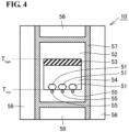
- the temperature difference method of the high-temperature high-pressure method is performed, for example, in a sample chamber with a structure illustrated in Fig. 4 .
- a sample chamber 10 used to manufacture a single-crystal diamond 51 includes an insulator 52, a carbon source 53, a solvent metal 54, and a diamond seed substrate 55 in a space surrounded by a graphite heater 57, and includes a pressure medium 56 outside the graphite heater 57.
- the temperature difference method is a synthesis method of providing a vertical temperature gradient in the sample chamber 10, placing the carbon source 53 in a high-temperature portion (T high ), placing the diamond seed substrate 55 in a low-temperature portion (T low ), placing the solvent metal 54 between the carbon source 53 and the diamond seed substrate 55, and growing the single-crystal diamond 51 on the diamond seed substrate 55 at a temperature not lower than the temperature at which the solvent metal 54 melts and at a pressure not lower than the pressure at which the diamond is thermally stable.
- the carbon source 53 is preferably a diamond powder. Graphite or pyrolytic carbon may also be used.
- the solvent metal 54 may be one or more metals selected from iron (Fe), cobalt (Co), nickel (Ni), manganese (Mn), and the like, or an alloy containing these metals.
- Titanium (Ti) is preferably added as a nitrogen getter to the solvent metal 54 at a concentration of 0.2% by mass or more. This can control the nitrogen content based on the number of atoms of the single-crystal diamond to be 50 ppm or less.
- Boron (B) is preferably added to the solvent metal 54 at a concentration of 2 ppm or more. This can control the boron content based on the number of atoms of the single-crystal diamond to be 0.01 ppm or more.
- a certain amount of titanium (Ti) can be added to the metal solvent as a nitrogen getter to intentionally leave nitrogen in the crystal. This makes it possible to control the nitrogen content of the crystal. This method is not employed in known temperature difference methods.
- the nitrogen content based on the number of atoms of a single-crystal diamond grown on the diamond seed substrate preferably ranges from 0.1 to 10 times the nitrogen content based on the number of atoms of the diamond seed substrate. This can reduce defects and distortion in the crystal due to the addition of nitrogen.
- a NV center in a single-crystal diamond can be formed, for example, by electron-beam irradiation with an energy of 3 MeV at a dose (electron-beam irradiation amount) of 3 ⁇ 10 17 cm -2 per 1 ⁇ 10 17 cm -3 of nitrogen concentration (nitrogen content based on the number of atoms) in the single-crystal diamond and then by annealing the single-crystal diamond in a vacuum at 900°C.
- the electron-beam irradiation dose is preferably increased for a sample with a high nitrogen content and is preferably decreased for a sample with a low nitrogen content.
- a method of manufacturing the single-crystal diamond according to the present embodiment includes preparing a seed substrate and growing a single-crystal diamond on the seed substrate by a high-temperature high-pressure synthesis method, wherein a main surface of the seed substrate has an inscribed circle diameter of more than 1.0 mm, the main surface has an etch-pit density of 1 ⁇ 10 5 /cm 2 or less, and the main surface of the seed substrate has two or less growth sectors.
- the half-width of a peak at a Raman shift in the range of 1332 cm -1 to 1333 cm -1 in a Raman spectrum of a single-crystal diamond was determined by measurement with a double monochromator Raman spectrometer at a wave number resolution of 0.5 cm -1 or less or with a LabRAM HR-800 (manufactured by HORIBA Jobin Yvon), and by conversion to the half-width of the diamond itself in consideration of the resolution of a light source and the apparatus.
- Example 1 Sample 1 to Sample 13, Sample 1-1, Sample 1-2]
- a diamond seed substrate is cut out from a single-crystal diamond material manufactured by the temperature difference method so as to include a single growth sector or a plurality of sectors, thereby preparing the diamond seed substrate A and the diamond seed substrate B described in the second embodiment.
- the type (A or B) and the size of the diamond seed substrate, the number of growth sectors in the diamond seed substrate, and the etch-pit density are shown in the columns of "Type", “Size”, “Number of growth sectors", and "Etch-pit density” of "Diamond seed substrate” in Table 1. [Table 1] Sample No.
- a single-crystal diamond is grown on the diamond seed substrate by the temperature difference method of the high-temperature high-pressure method to manufacture a single-crystal diamond of each sample.
- the temperature difference method is performed in a sample chamber with the structure illustrated in Fig. 4 .
- Ti is added as a nitrogen getter to the solvent in an amount described in "Ti addition amount" of "Synthesis conditions" in Table 1 (for example, 1.5% by mass of Ti is added in Sample 1).
- the single-crystal diamond was irradiated with an electron beam having an energy of 3 MeV at a dose of 3 ⁇ 10 17 cm -2 per 1 ⁇ 10 17 cm -3 of nitrogen concentration (nitrogen content based on the number of atoms) in the single-crystal diamond, and was then annealed in a vacuum at 900°C to manufacture a single-crystal diamond of each sample.
- ODMR optically detected magnetic resonance method
- the vertical axis of an ODMR spectrum represents the fluorescence intensity of NV -
- the horizontal axis represents the frequency of a microwave.
- a dip peak with low fluorescence intensity is detected at the frequency position (peak position) of resonance. It is known that this peak is shifted by a frequency corresponding to the magnetic field due to the Zeeman effect.
- a peak in an ODMR spectrum of a single-crystal diamond shows that an external magnetic field can be detected using the peak position, and the single-crystal diamond can be applied to a magnetic sensor.
- the column of "Average phase difference” shows the average of the phase difference in consideration of the thickness and the area described in the first embodiment
- the column of "13C” shows the concentration of the isotope 13 C of carbon
- the column of "Cutout size” shows the cutout size from a synthesized single-crystal diamond for evaluation of the items shown in Table 2
- the column of "Single sector” shows the single sector content described in the first embodiment
- the column of "ODMR” shows the half-width of a peak of ODMR. All the samples evaluated in Example 1 had a thicknesses of 0.4 mm.
- the nitrogen content of the single-crystal diamond in Sample 1 is measured by ESR to be 0.28 ppm.
- the boron content of the single-crystal diamond analyzed by SIMS is 0.0007 ppm.
- a Raman spectrum of the single-crystal diamond is measured with the double monochromator Raman spectrometer with a resolution of 0.5 cm -1 , and the half-width at 1332 cm -1 is found to be 1.60 cm -1 .
- a polarized light transmission image of the single-crystal diamond is observed with a polarized light transmission microscope. As a result of evaluating distortion, the average phase difference is 1 nm/mm.
- a diamond seed substrate is cut out from a single-crystal diamond material manufactured by the temperature difference method so as to include a single growth sector or a plurality of sectors, thereby preparing the diamond seed substrate A and the diamond seed substrate B described in the second embodiment.
- the type (A or B) and the size of the diamond seed substrate, the number of growth sectors in the diamond seed substrate, and the etch-pit density are shown in the columns of "Type", “Size”, “Number of growth sectors", and "Etch-pit density" of "Diamond seed substrate” in Table 3. [Table 3] Sample No.
- Methane gas with a carbon isotope 12 C concentration of 99.999% is passed through titanium sponge heated to 600°C or more to remove nitrogen from the methane gas.
- the methane gas from which nitrogen has been removed is blown onto a Ta substrate without Ni heated to a high temperature of 1900°C in a vacuum chamber.
- the methane gas is decomposed on the Ta substrate, forming graphite with a size of 10 mm ⁇ 10 mm and with a carbon isotope 12 C concentration of 99.999% or more on the Ta substrate.
- the graphite is used as a carbon source.
- a high-purity Fe-Co-Ti alloy containing a nitrogen getter in an amount described in "Ti addition amount" of "Synthesis conditions" in Table 3 (for example, 1.0% by mass in Sample 21) is prepared as a metal solvent.
- the heater surface is coated with graphite having a carbon isotope 12 C concentration of 99.999% or more.
- a diamond synthesis system in which a seed substrate, a solvent, and high-purity graphite with concentrated isotope as a carbon source are arranged in this order from the bottom is enclosed in a cup-shaped Fe cell without carbon or Ni, and the upper surface thereof is sealed in a vacuum of 10 -3 Pa or less.
- the single-crystal diamond was irradiated with an electron beam having an energy of 3 MeV at a dose of 3 ⁇ 10 17 cm -2 per 1 ⁇ 10 17 cm -3 of nitrogen concentration (nitrogen content based on the number of atoms) in the single-crystal diamond, and was then annealed in a vacuum at 900°C to manufacture a single-crystal diamond of each sample.
- the NV center content and ODMR were measured in the single-crystal diamond of each sample after the electron-beam irradiation.
- the nitrogen content of the single-crystal diamond is 0.42 ppm as measured by ESR
- the boron content of the single-crystal diamond is 0.0005 ppm when analyzed by SIMS
- the 13 C content of the single-crystal diamond is analyzed to be 0.002%.
- a Raman spectrum of the single-crystal diamond is measured with the double monochromator Raman spectrometer with a resolution of 0.5 cm -1 , and the half-width at 1332 cm -1 is found to be 1.60 cm -1 .
- a polarized light transmission image of the single-crystal diamond is observed with a polarized light transmission microscope. As a result of evaluating distortion, the average phase difference is 1 nm/mm.
- a diamond seed substrate is cut out from a single-crystal diamond material manufactured by the temperature difference method so as to include a single growth sector or a plurality of sectors, thereby preparing the diamond seed substrate C described in the second embodiment.
- the single-crystal diamond material is Sample 1, Sample 10, Sample 13, Sample 21, or Sample 22 prepared in Example 1 or Example 2.
- the type of the diamond seed substrate, the sample No. used for the single-crystal diamond material, the size, the number of growth sectors in the diamond seed substrate, and the etch-pit density are shown in the columns of "Type", “Single-crystal diamond material", “Size”, “Number of growth sectors", and "Etch-pit density” of "Diamond seed substrate” in Table 5. [Table 5] Sample No.
- a single-crystal diamond is grown on the diamond seed substrate by the temperature difference method to manufacture a single-crystal diamond of each sample.
- the temperature difference method is performed in a sample chamber with the structure illustrated in Fig. 4 .
- Ti is added as a nitrogen getter to the solvent in an amount described in "Ti addition amount" of "Synthesis conditions" in Table 5 (for example, 1.5% by mass is added in Sample 31).
- the single-crystal diamond was irradiated with an electron beam having an energy of 3 MeV at a dose of 3 ⁇ 10 17 cm -2 per 1 ⁇ 10 17 cm -3 of nitrogen concentration (nitrogen content based on the number of atoms) in the single-crystal diamond, and was then annealed in a vacuum at 900°C to manufacture a single-crystal diamond of each sample.
- the electron-beam irradiation negligibly changes the measurement results of the size, the half-width of an X-ray diffraction rocking curve, the half-width of a peak in a Raman spectrum, the etch-pit density, the number of defects identified in an X-ray topographic image, the average of the phase difference, the nitrogen content, the 13 C content, the boron content, the cutout size, and the single sector content of the single-crystal diamond.
Landscapes
- Chemical & Material Sciences (AREA)
- Organic Chemistry (AREA)
- Engineering & Computer Science (AREA)
- Crystallography & Structural Chemistry (AREA)
- Materials Engineering (AREA)
- Metallurgy (AREA)
- Life Sciences & Earth Sciences (AREA)
- General Life Sciences & Earth Sciences (AREA)
- Geology (AREA)
- Inorganic Chemistry (AREA)
- Chemical Kinetics & Catalysis (AREA)
- Crystals, And After-Treatments Of Crystals (AREA)
Applications Claiming Priority (2)
| Application Number | Priority Date | Filing Date | Title |
|---|---|---|---|
| JP2021061207 | 2021-03-31 | ||
| PCT/JP2022/016170 WO2022210934A1 (ja) | 2021-03-31 | 2022-03-30 | 単結晶ダイヤモンド及びその製造方法 |
Publications (2)
| Publication Number | Publication Date |
|---|---|
| EP4317545A1 true EP4317545A1 (de) | 2024-02-07 |
| EP4317545A4 EP4317545A4 (de) | 2024-11-06 |
Family
ID=83459575
Family Applications (1)
| Application Number | Title | Priority Date | Filing Date |
|---|---|---|---|
| EP22781144.5A Pending EP4317545A4 (de) | 2021-03-31 | 2022-03-30 | Einkristalliner diamant und herstellungsverfahren dafür |
Country Status (5)
| Country | Link |
|---|---|
| US (1) | US20240175167A1 (de) |
| EP (1) | EP4317545A4 (de) |
| JP (1) | JP7845354B2 (de) |
| CN (1) | CN116981802A (de) |
| WO (1) | WO2022210934A1 (de) |
Families Citing this family (4)
| Publication number | Priority date | Publication date | Assignee | Title |
|---|---|---|---|---|
| CN116997689A (zh) * | 2021-03-31 | 2023-11-03 | 住友电气工业株式会社 | 单晶金刚石及其制造方法 |
| WO2024176584A1 (ja) * | 2023-02-24 | 2024-08-29 | 国立研究開発法人量子科学技術研究開発機構 | 窒素-空孔複合欠陥を有する材料の製造方法、製造装置、製造プログラム、及び窒素-空孔複合欠陥を有する材料 |
| EP4692428A1 (de) * | 2023-04-03 | 2026-02-11 | Sumitomo Electric Industries, Ltd. | Synthetischer einkristalliner diamant, verfahren zur herstellung eines synthetischen einkristallinen diamanten und diamantsubstrat |
| WO2025204546A1 (ja) * | 2024-03-28 | 2025-10-02 | 住友電気工業株式会社 | 単結晶ダイヤモンド基板 |
Family Cites Families (15)
| Publication number | Priority date | Publication date | Assignee | Title |
|---|---|---|---|---|
| KR100269924B1 (ko) * | 1993-10-08 | 2000-11-01 | 하지메 히토추야나기 | 합성 다이아몬와 그 제조방법 |
| JP3339137B2 (ja) | 1993-10-27 | 2002-10-28 | 住友電気工業株式会社 | 合成ダイヤモンド単結晶およびその製造方法 |
| JP3456263B2 (ja) | 1993-10-08 | 2003-10-14 | 住友電気工業株式会社 | 歪みの少ない合成ダイヤモンドおよびその製造方法並びに合成ダイヤモンドの歪み測定方法 |
| JP4291886B2 (ja) * | 1994-12-05 | 2009-07-08 | 住友電気工業株式会社 | 低欠陥ダイヤモンド単結晶及びその合成方法 |
| GB0130005D0 (en) * | 2001-12-14 | 2002-02-06 | Diamanx Products Ltd | Boron doped diamond |
| JP4623356B2 (ja) * | 2003-12-02 | 2011-02-02 | 住友電気工業株式会社 | 単結晶ダイヤモンド |
| KR101240785B1 (ko) * | 2003-12-12 | 2013-03-07 | 엘리멘트 식스 리미티드 | 화학적 증착 다이아몬드에 마크를 통합시키는 방법 |
| WO2006048957A1 (ja) * | 2004-11-05 | 2006-05-11 | Sumitomo Electric Industries, Ltd. | 単結晶ダイヤモンド |
| JP5002982B2 (ja) * | 2005-04-15 | 2012-08-15 | 住友電気工業株式会社 | 単結晶ダイヤモンドの製造方法 |
| US9133566B2 (en) * | 2005-12-09 | 2015-09-15 | Element Six Technologies Limited | High crystalline quality synthetic diamond |
| GB0900771D0 (en) * | 2009-01-16 | 2009-03-04 | Element Six Ltd | Diamond |
| JP5891564B2 (ja) * | 2009-06-26 | 2016-03-23 | エレメント シックス リミテッド | ファンシーな淡い青色又はファンシーな淡い青色/緑色の単結晶cvdダイヤモンドの製造方法及び得られた製品 |
| GB201108644D0 (en) * | 2011-05-24 | 2011-07-06 | Element Six Ltd | Diamond sensors, detectors, and quantum devices |
| GB201904435D0 (en) * | 2019-03-29 | 2019-05-15 | Element Six Tech Ltd | Single crystal synthetic diamond material |
| JP7263201B2 (ja) | 2019-10-09 | 2023-04-24 | 株式会社アルバック | プラズマ装置、電源装置、プラズマ維持方法 |
-
2022
- 2022-03-30 WO PCT/JP2022/016170 patent/WO2022210934A1/ja not_active Ceased
- 2022-03-30 EP EP22781144.5A patent/EP4317545A4/de active Pending
- 2022-03-30 US US18/283,803 patent/US20240175167A1/en active Pending
- 2022-03-30 JP JP2023511506A patent/JP7845354B2/ja active Active
- 2022-03-30 CN CN202280020425.1A patent/CN116981802A/zh active Pending
Also Published As
| Publication number | Publication date |
|---|---|
| JPWO2022210934A1 (de) | 2022-10-06 |
| US20240175167A1 (en) | 2024-05-30 |
| EP4317545A4 (de) | 2024-11-06 |
| WO2022210934A1 (ja) | 2022-10-06 |
| CN116981802A (zh) | 2023-10-31 |
| JP7845354B2 (ja) | 2026-04-14 |
Similar Documents
| Publication | Publication Date | Title |
|---|---|---|
| EP4317545A1 (de) | Einkristalliner diamant und herstellungsverfahren dafür | |
| EP4317542A1 (de) | Einkristalldiamant und verfahren zur herstellung davon | |
| TWI408260B (zh) | 高結晶品質之合成鑽石 | |
| US8963070B2 (en) | Method for measuring carbon concentration in polycrystalline silicon | |
| Bolshakov et al. | Enhanced deposition rate of polycrystalline CVD diamond at high microwave power densities | |
| JP4291886B2 (ja) | 低欠陥ダイヤモンド単結晶及びその合成方法 | |
| EP3048641B1 (de) | Verfahren zur vorhersage des verzugs in monokristallinem siliziumcarbid-wafer | |
| KR20110046390A (ko) | 고체 상태 재료 | |
| JP2012121748A (ja) | ダイヤモンド及びこれを用いた磁気センサー | |
| EP4317540A1 (de) | Einkristalldiamant und verfahren zur herstellung davon | |
| WO2016114716A1 (en) | Electronic device grade single crystal diamonds and method of producing the same | |
| CN113423875A (zh) | 单晶合成金刚石材料 | |
| Spirito et al. | Lattice dynamics in chiral tellurium by linear and circularly polarized Raman spectroscopy: crystal orientation and handedness | |
| EP4317539A1 (de) | Einkristalldiamant und verfahren zur herstellung davon | |
| Churilov et al. | Purification, crystal growth and detector performance of TlBr | |
| EP3045570B1 (de) | Einkristalline diamanten für elektronische vorrichtungen und verfahren zur herstellung davon | |
| US11905620B2 (en) | Preparation and application of highly coherent diamond nitrogen vacancy and diamond anvil | |
| US12571126B2 (en) | Single-crystal diamond, method of manufacturing the same, and method of manufacturing single-crystal diamond plate | |
| EP4317544A1 (de) | Einkristalldiamant und diamantverbundstoff damit | |
| EP4357490A1 (de) | Synthetischer einkristalldiamant und herstellungsverfahren dafür | |
| TWI271450B (en) | Boron doped diamond | |
| CN120553702A (zh) | 一种磁共振对比度高的量子金刚石及其制备方法和应用 | |
| WO2025204546A1 (ja) | 単結晶ダイヤモンド基板 |
Legal Events
| Date | Code | Title | Description |
|---|---|---|---|
| STAA | Information on the status of an ep patent application or granted ep patent |
Free format text: STATUS: THE INTERNATIONAL PUBLICATION HAS BEEN MADE |
|
| PUAI | Public reference made under article 153(3) epc to a published international application that has entered the european phase |
Free format text: ORIGINAL CODE: 0009012 |
|
| STAA | Information on the status of an ep patent application or granted ep patent |
Free format text: STATUS: REQUEST FOR EXAMINATION WAS MADE |
|
| 17P | Request for examination filed |
Effective date: 20230915 |
|
| AK | Designated contracting states |
Kind code of ref document: A1 Designated state(s): AL AT BE BG CH CY CZ DE DK EE ES FI FR GB GR HR HU IE IS IT LI LT LU LV MC MK MT NL NO PL PT RO RS SE SI SK SM TR |
|
| DAV | Request for validation of the european patent (deleted) | ||
| DAX | Request for extension of the european patent (deleted) | ||
| A4 | Supplementary search report drawn up and despatched |
Effective date: 20241008 |
|
| RIC1 | Information provided on ipc code assigned before grant |
Ipc: B01J 3/06 20060101ALI20241001BHEP Ipc: C01B 32/26 20170101ALI20241001BHEP Ipc: C30B 29/04 20060101AFI20241001BHEP |