EP4318029A1 - Flut- und punktemitter - Google Patents
Flut- und punktemitter Download PDFInfo
- Publication number
- EP4318029A1 EP4318029A1 EP23188764.7A EP23188764A EP4318029A1 EP 4318029 A1 EP4318029 A1 EP 4318029A1 EP 23188764 A EP23188764 A EP 23188764A EP 4318029 A1 EP4318029 A1 EP 4318029A1
- Authority
- EP
- European Patent Office
- Prior art keywords
- light
- emitters
- channel
- light signal
- light source
- Prior art date
- Legal status (The legal status is an assumption and is not a legal conclusion. Google has not performed a legal analysis and makes no representation as to the accuracy of the status listed.)
- Withdrawn
Links
Images



Classifications
-
- G—PHYSICS
- G01—MEASURING; TESTING
- G01S—RADIO DIRECTION-FINDING; RADIO NAVIGATION; DETERMINING DISTANCE OR VELOCITY BY USE OF RADIO WAVES; LOCATING OR PRESENCE-DETECTING BY USE OF THE REFLECTION OR RERADIATION OF RADIO WAVES; ANALOGOUS ARRANGEMENTS USING OTHER WAVES
- G01S7/00—Details of systems according to groups G01S13/00, G01S15/00, G01S17/00
- G01S7/48—Details of systems according to groups G01S13/00, G01S15/00, G01S17/00 of systems according to group G01S17/00
- G01S7/483—Details of pulse systems
- G01S7/484—Transmitters
-
- G—PHYSICS
- G02—OPTICS
- G02B—OPTICAL ELEMENTS, SYSTEMS OR APPARATUS
- G02B5/00—Optical elements other than lenses
- G02B5/30—Polarising elements
- G02B5/3083—Birefringent or phase retarding elements
-
- G—PHYSICS
- G01—MEASURING; TESTING
- G01S—RADIO DIRECTION-FINDING; RADIO NAVIGATION; DETERMINING DISTANCE OR VELOCITY BY USE OF RADIO WAVES; LOCATING OR PRESENCE-DETECTING BY USE OF THE REFLECTION OR RERADIATION OF RADIO WAVES; ANALOGOUS ARRANGEMENTS USING OTHER WAVES
- G01S7/00—Details of systems according to groups G01S13/00, G01S15/00, G01S17/00
- G01S7/48—Details of systems according to groups G01S13/00, G01S15/00, G01S17/00 of systems according to group G01S17/00
- G01S7/481—Constructional features, e.g. arrangements of optical elements
- G01S7/4814—Constructional features, e.g. arrangements of optical elements of transmitters alone
- G01S7/4815—Constructional features, e.g. arrangements of optical elements of transmitters alone using multiple transmitters
-
- G—PHYSICS
- G01—MEASURING; TESTING
- G01S—RADIO DIRECTION-FINDING; RADIO NAVIGATION; DETERMINING DISTANCE OR VELOCITY BY USE OF RADIO WAVES; LOCATING OR PRESENCE-DETECTING BY USE OF THE REFLECTION OR RERADIATION OF RADIO WAVES; ANALOGOUS ARRANGEMENTS USING OTHER WAVES
- G01S17/00—Systems using the reflection or reradiation of electromagnetic waves other than radio waves, e.g. lidar systems
- G01S17/02—Systems using the reflection of electromagnetic waves other than radio waves
- G01S17/06—Systems determining position data of a target
- G01S17/08—Systems determining position data of a target for measuring distance only
-
- G—PHYSICS
- G01—MEASURING; TESTING
- G01S—RADIO DIRECTION-FINDING; RADIO NAVIGATION; DETERMINING DISTANCE OR VELOCITY BY USE OF RADIO WAVES; LOCATING OR PRESENCE-DETECTING BY USE OF THE REFLECTION OR RERADIATION OF RADIO WAVES; ANALOGOUS ARRANGEMENTS USING OTHER WAVES
- G01S17/00—Systems using the reflection or reradiation of electromagnetic waves other than radio waves, e.g. lidar systems
- G01S17/02—Systems using the reflection of electromagnetic waves other than radio waves
- G01S17/06—Systems determining position data of a target
- G01S17/08—Systems determining position data of a target for measuring distance only
- G01S17/32—Systems determining position data of a target for measuring distance only using transmission of continuous waves, whether amplitude-, frequency-, or phase-modulated, or unmodulated
-
- G—PHYSICS
- G01—MEASURING; TESTING
- G01S—RADIO DIRECTION-FINDING; RADIO NAVIGATION; DETERMINING DISTANCE OR VELOCITY BY USE OF RADIO WAVES; LOCATING OR PRESENCE-DETECTING BY USE OF THE REFLECTION OR RERADIATION OF RADIO WAVES; ANALOGOUS ARRANGEMENTS USING OTHER WAVES
- G01S17/00—Systems using the reflection or reradiation of electromagnetic waves other than radio waves, e.g. lidar systems
- G01S17/88—Lidar systems specially adapted for specific applications
- G01S17/89—Lidar systems specially adapted for specific applications for mapping or imaging
- G01S17/894—Three-dimensional [3D] imaging with simultaneous measurement of time-of-flight at a two-dimensional [2D] array of receiver pixels, e.g. time-of-flight cameras or flash lidar
-
- G—PHYSICS
- G01—MEASURING; TESTING
- G01S—RADIO DIRECTION-FINDING; RADIO NAVIGATION; DETERMINING DISTANCE OR VELOCITY BY USE OF RADIO WAVES; LOCATING OR PRESENCE-DETECTING BY USE OF THE REFLECTION OR RERADIATION OF RADIO WAVES; ANALOGOUS ARRANGEMENTS USING OTHER WAVES
- G01S7/00—Details of systems according to groups G01S13/00, G01S15/00, G01S17/00
- G01S7/48—Details of systems according to groups G01S13/00, G01S15/00, G01S17/00 of systems according to group G01S17/00
- G01S7/481—Constructional features, e.g. arrangements of optical elements
- G01S7/4811—Constructional features, e.g. arrangements of optical elements common to transmitter and receiver
- G01S7/4813—Housing arrangements
-
- G—PHYSICS
- G01—MEASURING; TESTING
- G01S—RADIO DIRECTION-FINDING; RADIO NAVIGATION; DETERMINING DISTANCE OR VELOCITY BY USE OF RADIO WAVES; LOCATING OR PRESENCE-DETECTING BY USE OF THE REFLECTION OR RERADIATION OF RADIO WAVES; ANALOGOUS ARRANGEMENTS USING OTHER WAVES
- G01S7/00—Details of systems according to groups G01S13/00, G01S15/00, G01S17/00
- G01S7/48—Details of systems according to groups G01S13/00, G01S15/00, G01S17/00 of systems according to group G01S17/00
- G01S7/499—Details of systems according to groups G01S13/00, G01S15/00, G01S17/00 of systems according to group G01S17/00 using polarisation effects
-
- G—PHYSICS
- G02—OPTICS
- G02B—OPTICAL ELEMENTS, SYSTEMS OR APPARATUS
- G02B1/00—Optical elements characterised by the material of which they are made; Optical coatings for optical elements
- G02B1/002—Optical elements characterised by the material of which they are made; Optical coatings for optical elements made of materials engineered to provide properties not available in nature, e.g. metamaterials
-
- G—PHYSICS
- G02—OPTICS
- G02B—OPTICAL ELEMENTS, SYSTEMS OR APPARATUS
- G02B27/00—Optical systems or apparatus not provided for by any of the groups G02B1/00 - G02B26/00, G02B30/00
- G02B27/09—Beam shaping, e.g. changing the cross-sectional area, not otherwise provided for
- G02B27/0938—Using specific optical elements
- G02B27/0944—Diffractive optical elements, e.g. gratings, holograms
-
- G—PHYSICS
- G02—OPTICS
- G02F—OPTICAL DEVICES OR ARRANGEMENTS FOR THE CONTROL OF LIGHT BY MODIFICATION OF THE OPTICAL PROPERTIES OF THE MEDIA OF THE ELEMENTS INVOLVED THEREIN; NON-LINEAR OPTICS; FREQUENCY-CHANGING OF LIGHT; OPTICAL LOGIC ELEMENTS; OPTICAL ANALOGUE/DIGITAL CONVERTERS
- G02F1/00—Devices or arrangements for the control of the intensity, colour, phase, polarisation or direction of light arriving from an independent light source, e.g. switching, gating or modulating; Non-linear optics
- G02F1/01—Devices or arrangements for the control of the intensity, colour, phase, polarisation or direction of light arriving from an independent light source, e.g. switching, gating or modulating; Non-linear optics for the control of the intensity, phase, polarisation or colour
-
- F—MECHANICAL ENGINEERING; LIGHTING; HEATING; WEAPONS; BLASTING
- F21—LIGHTING
- F21Y—INDEXING SCHEME ASSOCIATED WITH SUBCLASSES F21K, F21L, F21S and F21V, RELATING TO THE FORM OR THE KIND OF THE LIGHT SOURCES OR OF THE COLOUR OF THE LIGHT EMITTED
- F21Y2105/00—Planar light sources
- F21Y2105/10—Planar light sources comprising a two-dimensional [2D] array of point-like light-generating elements
- F21Y2105/14—Planar light sources comprising a two-dimensional [2D] array of point-like light-generating elements characterised by the overall shape of the two-dimensional [2D] array
- F21Y2105/16—Planar light sources comprising a two-dimensional [2D] array of point-like light-generating elements characterised by the overall shape of the two-dimensional [2D] array square or rectangular, e.g. for light panels
-
- G—PHYSICS
- G06—COMPUTING OR CALCULATING; COUNTING
- G06V—IMAGE OR VIDEO RECOGNITION OR UNDERSTANDING
- G06V10/00—Arrangements for image or video recognition or understanding
- G06V10/10—Image acquisition
- G06V10/12—Details of acquisition arrangements; Constructional details thereof
- G06V10/14—Optical characteristics of the device performing the acquisition or on the illumination arrangements
- G06V10/145—Illumination specially adapted for pattern recognition, e.g. using gratings
-
- G—PHYSICS
- G06—COMPUTING OR CALCULATING; COUNTING
- G06V—IMAGE OR VIDEO RECOGNITION OR UNDERSTANDING
- G06V40/00—Recognition of biometric, human-related or animal-related patterns in image or video data
- G06V40/10—Human or animal bodies, e.g. vehicle occupants or pedestrians; Body parts, e.g. hands
- G06V40/16—Human faces, e.g. facial parts, sketches or expressions
- G06V40/161—Detection; Localisation; Normalisation
-
- H—ELECTRICITY
- H01—ELECTRIC ELEMENTS
- H01S—DEVICES USING THE PROCESS OF LIGHT AMPLIFICATION BY STIMULATED EMISSION OF RADIATION [LASER] TO AMPLIFY OR GENERATE LIGHT; DEVICES USING STIMULATED EMISSION OF ELECTROMAGNETIC RADIATION IN WAVE RANGES OTHER THAN OPTICAL
- H01S5/00—Semiconductor lasers
- H01S5/005—Optical components external to the laser cavity, specially adapted therefor, e.g. for homogenisation or merging of the beams or for manipulating laser pulses, e.g. pulse shaping
-
- H—ELECTRICITY
- H01—ELECTRIC ELEMENTS
- H01S—DEVICES USING THE PROCESS OF LIGHT AMPLIFICATION BY STIMULATED EMISSION OF RADIATION [LASER] TO AMPLIFY OR GENERATE LIGHT; DEVICES USING STIMULATED EMISSION OF ELECTROMAGNETIC RADIATION IN WAVE RANGES OTHER THAN OPTICAL
- H01S5/00—Semiconductor lasers
- H01S5/02—Structural details or components not essential to laser action
- H01S5/022—Mountings; Housings
- H01S5/0225—Out-coupling of light
- H01S5/02257—Out-coupling of light using windows, e.g. specially adapted for back-reflecting light to a detector inside the housing
-
- H—ELECTRICITY
- H01—ELECTRIC ELEMENTS
- H01S—DEVICES USING THE PROCESS OF LIGHT AMPLIFICATION BY STIMULATED EMISSION OF RADIATION [LASER] TO AMPLIFY OR GENERATE LIGHT; DEVICES USING STIMULATED EMISSION OF ELECTROMAGNETIC RADIATION IN WAVE RANGES OTHER THAN OPTICAL
- H01S5/00—Semiconductor lasers
- H01S5/10—Construction or shape of the optical resonator, e.g. extended or external cavity, coupled cavities, bent-guide, varying width, thickness or composition of the active region
- H01S5/18—Surface-emitting [SE] lasers, e.g. having both horizontal and vertical cavities
- H01S5/183—Surface-emitting [SE] lasers, e.g. having both horizontal and vertical cavities having only vertical cavities, e.g. vertical cavity surface-emitting lasers [VCSEL]
Definitions
- the present disclosure is directed to illumination systems for sensors, such as time-of-flight sensors.
- Integrated optical components providing functionalities, such as face recognition, proximity detection, and ambient light sensing, have become common in mobile devices, laptops, appliances, and many other types of devices.
- Such functionalities are often implemented with distance or depth sensors, such as time-of-flight (ToF) sensors, that determine a distance between the sensor and a target object by measuring the time a light signal takes to travel to the target object and back to the sensor.
- ToF time-of-flight
- the light signal emitted by a distance sensor is provided by an illumination system having a light emitter, such as a vertical-cavity surface-emitting laser (VCSEL).
- a light emitter such as a vertical-cavity surface-emitting laser (VCSEL).
- the light illumination system is either a flood illuminator or a dot projector, depending on the application of the distance sensor.
- Flood illuminators emit a strong flash that spreads light over a large region of space. Since the emitted power of the light signal is spread over a large area, the detecting capability of a distance sensor with a flood illuminator is limited to a short distance. As such, flood illuminators are often used to establish a focusing distance or the nature of a target object.
- dot projectors emit light in concentrated areas. As light is concentrated to certain areas, the detecting capability of a distance sensor with a dot projector is much further compared to a distance sensor with a flood illuminator. As such, dot projectors are often used to detect distal objects, and to precisely determine whether a target object corresponds to an authorized person.
- the present disclosure is directed to a sensor, such as a time-of-flight sensor, configured to switch between two different light patterns: a flood illumination pattern and a dot projection pattern.
- a sensor such as a time-of-flight sensor
- the sensor disclosed herein utilizes a single light source and a single optic to project the flood illumination pattern and the dot illumination pattern.
- the light source is, for example, a vertical-cavity surface-emitting laser that includes a dual channel array of polarized emitters.
- Channel 1 of the light source emits light with a first polarization (e.g. , transverse magnetic (TM) polarized light), and channel 2 of the light source emits light with a second polarization (e.g. , transverse electric (TE) polarized light) orthogonal to the first polarization.
- the channel 1 and channel 2 emitters are arranged in columns that alternate with each other.
- the light transmitted by the light source is transmitted through the optic.
- the optic is a polarization sensitive metaoptic that includes a plurality of asymmetrical meta-elements. The dimensions of the asymmetrical meta-elements are selected to provide the proper phase retardation to generate the dot projection pattern when Channel 1 is active, and generate the flood illumination pattern when Channel 2 is active.
- the present disclosure is directed to an optical sensor configured to switch between two different operational illuminations: flood illumination and dot projection.
- the device employs a single two-channel light source with one channel for each of two orthogonal polarization states; a metasurface-based polarization sensitive optic on a transmission side of the device, and an optic and detector on a reception side of the device.
- the illumination pattern can be chosen by the selection of the relative light source channel, with the same metasurface-based polarization sensitive optic projecting one of the two illuminations as a function of the light source polarization state.
- FIG. 1 is a sensor 10 according to an embodiment disclosed herein.
- the sensor 10 is a distance or depth sensor, such as a time-of-flight (ToF) sensor, that determines distances between the sensor 10 and a target object external to the sensor 10.
- the sensor 10 may be included in various electronic devices (e.g. , mobile handsets, cameras, tablets, laptops, and computers) for a variety of different applications, such as face recognition, proximity detection, and ambient light sensing. It is noted that the embodiments discussed herein may also be applied to other types of optical devices that utilize flood illumination and dot projection.
- the sensor 10 includes a substrate 12, a body 14, a light source 16, a transmission optical structure 18, a detector 20, and a reception optical structure 22.
- the substrate 12 provides a support platform for the sensor 10.
- the body 14, the light source 16, the transmission optical structure 18, the detector 20, and the reception optical structure 22 are positioned on the substrate 12.
- the substrate may be any type of rigid material, such as plastic, metal, glass, and semiconductor material.
- the substrate 12 is a printed circuit board that includes one or more electrical components (e.g. , capacitors, transistors, processors, etc.).
- the body 14 is positioned on the substrate 12.
- the substrate 12 and the body 14 protect the light source 16, the transmission optical structure 18, the detector 20, and the reception optical structure 22 from an external environment.
- the body 14 includes an output aperture 24 and an input aperture 26.
- the output aperture 24 directly overlies and is aligned with the light source 16 and the transmission optical structure 18.
- the output aperture 24 provides a hole for a light signal 28 to pass through.
- the light signal 28 is emitted from the light source 16, and directed to the target object in which a distance between the target object and the sensor 10 is being determined.
- the light signal 28 has a flood illumination pattern and/or a dot projection pattern upon being transmitted through the transmission optical structure 18.
- the input aperture 26 directly overlies and is aligned with the detector 20 and the reception optical structure 22.
- the input aperture 26 provides a hole for a light signal 30 to pass through.
- the light signal 30 is the light signal 28 reflected off of the target object.
- the light source 16 is positioned on the substrate 12.
- the light source 16 directly underlies and is aligned with the transmission optical structure 18 and the output aperture 24.
- the light source 16 emits the light signal 28 through the transmission optical structure 18 and the output aperture 24.
- the light source 16 is a vertical-cavity surface-emitting laser (VCSEL).
- VCSEL vertical-cavity surface-emitting laser
- the light source 16 is a dual channel light source that switches between a first channel that emits a first light signal having a first polarization state, and a second channel that emits a second light signal having a second polarization state orthogonal to the first polarization state.
- the transmission optical structure 18 directly overlies the light source 16 and is aligned with the light source 16 and the output aperture 24. In one embodiment, the transmission optical structure 18 covers the entire output aperture 24. In one embodiment, the transmission optical structure 18 is physically coupled to the body 14.
- the transmission optical structure 18 is a metasurface-based polarization sensitive optic with dual optical functions. Namely, the transmission optical structure 18 receives the light signal 28 transmitted by the light source 16, and produces a flood illumination pattern or a dot projection pattern depending on the current polarization state of the light signal 28. The transmission optical structure 18 will be discussed in further detail below.
- the detector 20 is positioned on the substrate 12.
- the detector 20 directly underlies and is aligned with the reception optical structure 22 and the input aperture 26.
- the detector 20 is integrated into a semiconductor substrate 32.
- the substrate 32 may also include other various electrical components (e.g. , transistors, capacitors, resistors, processors, etc.) and devices (e.g. , a reference sensor array).
- the detector 20 receives the light signal 30, which is the light signal 28 reflected off of the target object and passing through the input aperture 26 and the reception optical structure 22.
- the detector 20 includes a plurality of photodetectors that sense or measure the light signal 30.
- the detector 20 may be any type of sensor that measures light signals.
- the detector 20 is a single-photon avalanche diode (SPAD) array.
- SPAD single-photon avalanche diode
- the reception optical structure 22 directly overlies the detector 20 and is aligned with the detector 20 and the input aperture 26. In one embodiment, the reception optical structure 22 covers the entire input aperture 26. In one embodiment, the reception optical structure 22 is physically coupled to the body 14.
- the sensor 10 determines a distance between the sensor 10 and the target object in a surrounding environment.
- the light source 16 transmits the light signal 28 through the transmission optical structure 18 and the output aperture 24, and at the target object.
- the detector 20 receives and measures the light signal 30, which is the light signal 28 that hits the target object and is reflected back through input aperture 26 and the reception optical structure 22.
- the sensor 10 determines the time of flight of the light signal 28 to travel from the light source 16, to the target object, and back to the detector 20; and distances between the sensor 10 and the target object based on the time of flight.
- the determined distances may then be processed for further applications, such as face recognition, proximity detection, and ambient light sensing.
- the distances measured by the sensor 10 may be used to create a virtual profile reconstructions of a user of a device including the sensor 10.
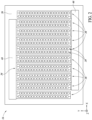
- Figure 2 is the light source 16, more specifically a top view of the light source 16, according to an embodiment disclosed herein.
- the light source 16 will be discussed with reference to the x-axis; the y-axis, which is transverse to the x-axis; and the z-axis, which is transverse to the x-axis and the y-axis, as shown in Figure 2 .
- the light source 16 emits the light signal 28 through the transmission optical structure 18 and the output aperture 24.
- the light source 16 includes a plurality of emitters 34 on a substrate 36.
- the substrate 36 may be a semiconductor substrate, printed circuit board, or another type of supporting structure.
- Each of the emitters 34 emits light to form a light signal, such as the light signal 28 in Figure 1 .
- the emitters 34 emit light in a direction along the z-axis. Stated differently, the light emitted by each of the emitters 34 propagates out of the page.
- the emitters 34 are arranged as an array in a number of columns 38 positioned along the x-axis, with each of the columns 38 extending along the y-axis.
- Each of the columns 38 of emitters includes one or more sub-columns 39 of emitters.
- the emitters of each sub-column 39 are aligned with each other along the y-axis.
- each of the columns include two sub-columns of emitters.
- the emitters of a first sub-column are staggered in position with the emitters of a second sub-column. Stated differently, the emitters of the first sub-column are unaligned with the emitters of a second sub-column along the x-axis such that an emitter of the second sub-column is positioned between two emitters of the first sub-column.
- the light source 16 is a two-channel light source that switches between first and second channels.
- Figure 3 shows a first channel 40 of the light source 16 according to an embodiment disclosed herein.
- Figure 4 shows a second channel 42 of the light source 16 according to an embodiment disclosed herein. It is beneficial to review Figures 3 and 4 together.
- the first channel 40 is formed by a first set of columns 41 of emitters that are electrically coupled to each other by a connector 44.
- the emitters of the first channel 40 emit light in response to an electrical signal being applied to the connector 44.
- the second channel 42 is formed by a second set of columns 43 that are electrically coupled to each other by a connector 46.
- the emitters of the second channel 42 emit light in response to an electrical signal being applied to the connector 46.
- the connector 44 is spaced from the connector 46 by the emitters of the first channel 40 and the second channel 42.
- the emitters of the first channel 40 and the second channel 42 are arranged on the substrate 36 in alternating, interleaved fashion. Namely, each column of the first set of columns 41 of emitters for the first channel 40 is spaced from another column of the first set of columns 41 along the x-axis by a column of the second set of columns 43 of emitters for the second channel 42. As a result, the emitters of the first channel 40 and the second channel 42 are not concentrated to a single area, and are able to emit light evenly across the substrate 36.
- the emitters of the first channel 40 emit a light signal having a first polarization state.
- the emitters of the first channel 40 emit a transverse magnetic (TM) polarized light signal with a magnetic field transverse to a propagation direction of the light signal.
- the emitters of the second channel 42 emit a light signal having a second polarization state orthogonal to the first polarization state.
- the emitters of the second channel 42 emit a transverse electric (TE) polarized light signal with an electric field transverse to the propagation direction of the light signal and transverse to the magnetic field of the light signal emitted by emitters of the first channel 40.
- the light source 16 includes one array per orthogonal polarization state.
- the emitters of the first channel 40 and the second channel 42 have a wavelength between 900 and 1000 nanometers.
- the light signal 28 before entering the transmission optical structure 18 has the first polarization state.
- the light signal 28 before entering the transmission optical structure 18 has the second polarization state.
- Figure 5 is a top view of the transmission optical structure 18 according to an embodiment disclosed herein.
- Figure 6 is an angled view of the transmission optical structure 18 according to an embodiment disclosed herein. It is beneficial to review Figures 5 and 6 together.
- the transmission optical structure 18 will be discussed with reference to the x-axis, the y-axis, and the z-axis as shown in Figures 5 and 6 .
- the transmission optical structure 18 receives the light signal 28 transmitted by the light source 16, and produces a flood illumination pattern or a dot projection pattern depending on the current polarization state of the light signal 28.
- the transmission optical structure 18 is a metasurface-based polarization sensitive optic with dual optical functions.
- transmission optical structures are implemented with diffractive optical elements (DOE) in ultrathin semiconductor that opportunely manipulate a light source output wave front into a specific far field intensity profile, such as flood or dot.
- DOE diffractive optical elements
- subwavelength dielectric nanostructures have become a remarkable candidate as technological platform for DOE, as optical metasurfaces are compatible with semiconductor fabrication processes ( e.g. , lithography), provide a potentially large number of phase quantization levels, and are suitable for the implementation of a variety of optical elements.
- a polarization dependence can be also achieved, providing the possibility to encode different distinctive functionalities to the same optics, accessible by the selection of a proper input polarization state.
- the transmission optical structure 18 includes an array of asymmetrical nano meta-elements 21.
- the meta-elements 21 are, for example, pillar structures, which in this embodiment are elliptical pillars. Other asymmetrical shapes are also possible.
- the meta-elements 21 have various dimensions. For example, as shown in Figures 5 and 6 , a first set of the meta-elements21 have lengths extending along the x-axis, a second set of the meta-elements21 have lengths extending along the y-axis, and a third set of the pillars are circular with substantially equal dimensions along the x-axis and the y-axis.
- the meta-elements 21 are fabricated by employing semiconductor processes, such as deep UV photolithography.
- the meta-elements 21 are not encapsulated and surrounded by, for example, air. In one embodiment, the meta-elements 21 are encapsulated by encapsulation material 23. The meta-elements 21 extend from a lower surface 25 of the encapsulation material 23 to an upper surface 27, which is opposite to the lower surface 25, of the encapsulation material 23. The transmission optical structure 18 is positioned in the sensor 10 such that the meta-elements 21 extend in the propagation direction of the light signal 28.
- the meta-elements 21 and the encapsulation material 23 are made of one or more dielectric materials.
- the meta-elements21 and the encapsulation material 23 are made of different materials.
- the meta-elements 21 and/or the encapsulation material 23 may include one or more of the following: silicon (Si), silicon dioxide, (SiO2), zinc sulphide (ZnS), galium nitride (GaN), zinc selenide (ZnSe), titanium dioxide (TiO2), silicon carbide (SiC), gallium phosphide (GaP), gallium arsenide (GaAs), and hydrogenated silicon (Si:H).
- the delta between the refractive index of the material of the meta-elements 21 and the refractive index of the material of the encapsulation material 23 is between 1.5 and 2.
- the mapping process may generally include simultaneously minimizing the delta between (1) the desired phase retardation to generate the flood illumination and dot projection in specific optic coordinates and (2) the phase retardation provided in both the first and second polarizations (TM and TE polarization) of the lights source 16 by the meta-elements 21, represented by the meta-element dimensions along the x-axis and y axis.
- each of the meta-elements 21 displays a different optical behavior (e.g. , transmission, phase retardation, etc.) as a function of incident polarization state (e.g ., TM or TE polarization) of the received light signal and the dimensions of the meta-elements along the x-axis and y-axis.
- incident polarization state e.g ., TM or TE polarization
- the dimensions of the meta-elements 21 along the x-axis and y axis are optimized to provide the proper phase retardation to generate a dot projection pattern from the light generated by the first channel 40 of the light source 16, and provide the proper phase retardation to generate a flood illumination pattern from the light generated by the second channel 42 of the light source 16.
- the dimensions of the meta-elements 21 along the x-axis and y axis are selected to alter the phase of the light transmitted by the first channel 40 to transform the light in to a dot projection pattern, and to alter the phase of the light transmitted by the second channel 42 to transform the light in to a flood illumination pattern.
- the emitters of the first channel 40 emit a light signal having a first polarization state, such as TM polarized light; and the emitters of the second channel 42 emit a light signal having a second polarization state orthogonal to the first polarization state, such as TE polarized light.
- the transmission optical structure 18 projects one of flood illumination and dot projection as a function of the polarization state of the light emitted by the light source 16. Namely, the transmission optical structure 18 projects a dot projection pattern upon receiving TM polarized light generated by the first channel, and projects a flood illumination pattern upon receiving TE polarized light generated by the second channel. Accordingly, dot projection and flood illumination may be chosen by selection of the first channel 40 or the second channel 42, respectively, of the light source 16.
- Figure 7 is a dot projection pattern 45 according to an embodiment disclosed herein.
- light is concentrated to certain areas.
- light is concentrated into an array of light including a plurality of columns and rows of light.
- Other patterns of concentrated light are also possible.
- the dot pattern may correspond to a replication of a VSCEL emitter layout according to the transmission optic function.
- the detecting capability of the sensor 10 while utilizing the dot projection pattern is much further compared to utilizing the flood illumination pattern.
- the sensor 10 may employ dot projection for applications that utilizes long distance detections, such as detecting distal objects.
- FIG 8 is a flood illumination pattern 47 according to an embodiment disclosed herein. As shown in Figure 8 , light is spread over a large region of space. Since the emitted power of the light signal is spread over a large area, the detecting capability of the sensor 10 while utilizing the flood illumination pattern is limited to a short distance. As such, the sensor 10 may employ flood illumination for applications that utilizes short distance detections, such as establishing a focusing distance or the nature of a proximal target object.
- Figure 9 is a flow diagram for dot projection according to an embodiment disclosed herein.
- step 48 the first channel 40 of the light source 16 is activated and the second channel 42 is deactivated.
- the emitters of the first channel 40 emit a light signal having a first polarization state, which in the embodiment shown in Figure 9 is TM polarized light.
- the second channel 42 has been removed from Figure 9 for illustrative purposes. The second channel 42 remains in the light source 16 as shown in Figures 2 to 4 , but is inactivated.
- the TM polarized light such as a pulse of the TM polarized light
- a far field intensity having the dot projection pattern 45 is emitted from the transmission optical structure 18.
- the dimensions of the meta-elements 21 of the transmission optical structure 18 are optimized to provide the proper phase retardation to generate the dot projection pattern from the light generated by the first channel 40, which in this embodiment is TM polarized light, maximizing at the same time the output transmission.
- the dot projection is transmitted on to a target object, which in this embodiment is a user's face, and reflected off of the target object.
- the reflected light is transmitted through the reception optical structure 22, and received by the detector 20.
- the detector 20 includes a plurality of photodetectors that sense or measure the reflected light signal.
- step 54 signal processing is performed on the detected light to determine distances between the sensor 10 and the target object, and generate further data depending on the application of the sensor 10, such a virtual profile reconstruction of the user's face for user authentication.
- Figure 10 is a flow diagram for flood illumination according to an embodiment disclosed herein.
- step 56 the second channel 42 of the light source 16 is activated and the first channel 40 is deactivated.
- the emitters of the second channel 42 emit a light signal having a second polarization state orthogonal to the first polarization state, which in the embodiment shown in Figure 9 is TE polarized light.
- the first channel 40 has been removed from Figure 10 for illustrative purposes. The first channel 40 remains in the light source 16 as shown in Figures 2 to 4 , but is inactivated.
- the TE polarized light such as a pulse of the TE polarized light
- a far field intensity having the flood illumination pattern 47 is emitted from the transmission optical structure 18.
- the dimensions of the meta-elements 21 of the transmission optical structure 18 are optimized to provide the proper phase retardation to generate the flood illumination pattern from the light generated by the second channel 42, which in this embodiment is TE polarized light.
- step 60 the dot projection is transmitted on to a target object, which in this embodiment is a user's face, and reflected off of the target object.
- the reflected light is transmitted through the reception optical structure 22, and received by the detector 20.
- the detector 20 includes a plurality of photodetectors that sense or measure the reflected light signal.
- step 62 signal processing is performed on the detected light to determine distances between the sensor 10 and the target object, and generate further data depending on the application of the sensor 10, such as a virtual profile reconstruction of the user's face or to establish focusing distance.
- the light source 16 and the transmission optical structure 18 are configured for flood illumination and dot projection.
- other types of light patterns are also possible.
- the dimensions of the meta-elements 21 of the transmission optical structure 18 may be optimized to provide the phase retardation to generate a circular, conical, or another shape based on the polarization of the light source 16.
- a single light source and a single transmission optical structure are employed.
- a first module including a first light source and a first transmission optical structure may be used to generate flood illumination
- a second module including a second light source and a second transmission optical structure may be used to generate dot projection.
- a device may be summarized as including a light source including a first plurality of emitters configured to transmit a first light signal having a first polarization state, and a second plurality of emitters configured to transmit a second light signal having a second polarization state transverse to the first polarization state; and an optic configured to receive the first light signal and generate a first light pattern with the first light signal, and receive the second light signal and generate a second light pattern with the second light signal.
- the first polarization state may be linear and the second polarization state may be orthogonal to the first polarization state.
- the first plurality of emitters may be arranged in a first plurality of columns
- the second plurality of emitters may be arranged in a second plurality of columns
- each column of the first plurality of columns may be spaced from another column of the first plurality of columns by a column of the second plurality of columns.
- the light source may include a first connector that electrically couples the first plurality of emitters to each other, and a second connector that electrically couples the second plurality of emitters to each other.
- the first connector may be spaced from the second connector by the first plurality of emitters and the second plurality of emitters.
- the optic may include a plurality of meta-elements that may extend in a propagation direction of the first light signal and the second light signal.
- the plurality of meta-elements may have an asymmetrical shape.
- Each of the plurality of meta-elements may have an elliptical shape.
- the plurality of meta-elements may include a first set of meta-elements having lengths extending in a first direction, and a second set of meta-elements having lengths extending in a second direction transverse to the first direction.
- the plurality of meta-elements may be made of a first material, and may be encapsulated with a second material.
- the first light pattern may be a flood illumination pattern
- the second light pattern may be a dot projection pattern
- a method may be summarized as including activating a first channel of a light source; transmitting, by the first channel of the light source, a first light signal having a first polarization state; generating, by an optic, a first light pattern with the first light signal; activating a second channel of the light source; transmitting, by the second channel of the light source, a second light signal having a second polarization state transverse to the first polarization state; and generating, by the optic, a second light pattern different from the first light pattern with the second light signal.
- the first polarization state may be linear, and the second polarization state may be orthogonal to the first polarization state.
- the first channel may include a first plurality of emitters arranged in a first plurality of columns
- the second channel may include a second plurality of emitters arranged in a second plurality of columns
- each column of the first plurality of columns may be spaced from another column of the first plurality of columns by a column of the second plurality of columns.
- the first light pattern may be a flood illumination pattern
- the second light pattern may be a dot projection pattern
- the optic may include a plurality of meta-elements that are asymmetrical shape.
- a device may be summarized as including a light source including a first channel and a second channel, the first channel including a first plurality of emitters configured to transmit a first light signal having a first polarization, the second channel including a second plurality of emitters configured to transmit a second light signal having a second polarization transverse to the first polarization; and an optic configured to alter a phase of the first light signal to produce a first light pattern, and a phase of the second light signal to produce a second light pattern different from the first light pattern.
- the first polarization may be linear, and the second polarization may be orthogonal to the first polarization.
- the first light pattern may be a flood illumination pattern
- the second light pattern may be a dot projection pattern
- the optic may include a plurality of meta-elements that extend in a propagation direction of the first light signal and the second light signal.
- the various embodiments disclosed herein provide a sensor configured to transmit a flood illumination pattern and a dot projection pattern.
- the sensor utilizes a single dual channel light source configured to switch between first and second polarizations, and a single polarization sensitive metaoptic that outputs the dot projection and the flood illumination in response to receiving the first polarization and the second polarization, respectively.
Landscapes
- Physics & Mathematics (AREA)
- Engineering & Computer Science (AREA)
- General Physics & Mathematics (AREA)
- Computer Networks & Wireless Communication (AREA)
- Radar, Positioning & Navigation (AREA)
- Remote Sensing (AREA)
- Electromagnetism (AREA)
- Optics & Photonics (AREA)
- Nonlinear Science (AREA)
- Optical Radar Systems And Details Thereof (AREA)
- General Engineering & Computer Science (AREA)
- Spectroscopy & Molecular Physics (AREA)
Applications Claiming Priority (1)
| Application Number | Priority Date | Filing Date | Title |
|---|---|---|---|
| US17/881,236 US12474516B2 (en) | 2022-08-04 | 2022-08-04 | Flood and dot emitter |
Publications (1)
| Publication Number | Publication Date |
|---|---|
| EP4318029A1 true EP4318029A1 (de) | 2024-02-07 |
Family
ID=87553868
Family Applications (1)
| Application Number | Title | Priority Date | Filing Date |
|---|---|---|---|
| EP23188764.7A Withdrawn EP4318029A1 (de) | 2022-08-04 | 2023-07-31 | Flut- und punktemitter |
Country Status (3)
| Country | Link |
|---|---|
| US (1) | US12474516B2 (de) |
| EP (1) | EP4318029A1 (de) |
| CN (1) | CN117518134A (de) |
Cited By (1)
| Publication number | Priority date | Publication date | Assignee | Title |
|---|---|---|---|---|
| EP4579316A1 (de) * | 2023-12-28 | 2025-07-02 | Himax Technologies Limited | Multifunktionsprojektor |
Citations (3)
| Publication number | Priority date | Publication date | Assignee | Title |
|---|---|---|---|---|
| EP3480555A1 (de) * | 2017-11-07 | 2019-05-08 | Samsung Electronics Co., Ltd. | Meta-projektor und elektronische vorrichtungen damit |
| US20200033710A1 (en) * | 2018-07-24 | 2020-01-30 | Qualcomm Incorporated | Adjustable light distribution for active depth sensing systems |
| US20200271941A1 (en) * | 2017-08-31 | 2020-08-27 | Metalenz, Inc. | Transmissive Metasurface Lens Integration |
Family Cites Families (28)
| Publication number | Priority date | Publication date | Assignee | Title |
|---|---|---|---|---|
| US6963598B1 (en) | 2000-05-23 | 2005-11-08 | Finisar Corporation | System and method for VCSEL polarization control |
| TWI381191B (zh) | 2007-12-03 | 2013-01-01 | Au Optronics Corp | 立體顯示器及其製作方法 |
| US8444275B2 (en) | 2010-08-12 | 2013-05-21 | Eastman Kodak Company | Light source control for projector with multiple pulse-width modulated light sources |
| CN103389534B (zh) | 2012-05-08 | 2016-04-13 | 香港科技大学 | 偏振转换器和偏振转换系统 |
| TWI617841B (zh) | 2014-10-22 | 2018-03-11 | 英特爾股份有限公司 | 用於光學系統的防雲紋圖樣擴散器 |
| US9459352B2 (en) * | 2014-11-20 | 2016-10-04 | Texas Instruments Incorporated | Multi-sensor proximity sensing using a near zone light sensor and a far zone light sensor |
| CN108604053B (zh) | 2015-10-21 | 2021-11-02 | 普林斯顿光电子股份有限公司 | 编码图案投影仪 |
| US11300453B2 (en) | 2017-06-18 | 2022-04-12 | William N. Carr | Photonic- and phononic-structured pixel for electromagnetic radiation and detection |
| CN109891187A (zh) | 2016-08-18 | 2019-06-14 | 特拉维夫大学拉莫特有限公司 | 结构光投影仪 |
| WO2018039273A1 (en) | 2016-08-22 | 2018-03-01 | Magic Leap, Inc. | Dithering methods and apparatus for wearable display device |
| US11303859B2 (en) | 2016-09-29 | 2022-04-12 | Stmicroelectronics (Research & Development) Limited | Time of flight sensing for brightness and autofocus control in image projection devices |
| CN109085733A (zh) * | 2017-06-13 | 2018-12-25 | 艾优优(深圳)技术有限公司 | 多组激光光源装置 |
| US10310362B2 (en) | 2018-06-29 | 2019-06-04 | Intel Corporation | LED pattern projector for 3D camera platforms |
| US10916023B2 (en) | 2018-09-14 | 2021-02-09 | Facebook Technologies, Llc | Depth measurement assembly with a structured light source and a time of flight camera |
| WO2020057124A1 (zh) | 2018-09-19 | 2020-03-26 | 青岛海信激光显示股份有限公司 | 一种激光器阵列、激光光源及激光投影设备 |
| US11092719B1 (en) * | 2019-01-29 | 2021-08-17 | Facebook Technologies, Llc | Dynamic dot array illuminators |
| EP4004686B1 (de) | 2019-07-26 | 2024-11-20 | Google LLC | Authentifizierungsverwaltung durch imu und radar |
| US11467672B2 (en) | 2019-08-30 | 2022-10-11 | Google Llc | Context-sensitive control of radar-based gesture-recognition |
| US11632448B2 (en) | 2019-12-03 | 2023-04-18 | Apple Inc. | Handheld electronic device |
| US11619828B2 (en) * | 2020-01-17 | 2023-04-04 | Stmicroelectronics (Research & Development) Limited | Transmission beam splitter |
| US11762212B2 (en) | 2020-03-12 | 2023-09-19 | Stmicroelectronics (Research & Development) Limited | Diffuse illumination system having VCSEL emitters and array of nanostructures |
| WO2021198269A1 (en) * | 2020-03-31 | 2021-10-07 | Trumpf Photonic Components Gmbh | Illumination device for a distance measurement camera system, a corresponding illumination method and a tof camera system |
| US11604975B2 (en) | 2020-04-09 | 2023-03-14 | Apple Inc. | Ternary mode of planar engine for neural processor |
| US11710945B2 (en) * | 2020-05-25 | 2023-07-25 | Apple Inc. | Projection of patterned and flood illumination |
| CN115117735A (zh) * | 2021-03-17 | 2022-09-27 | 上海禾赛科技有限公司 | 激光器、光源模组及激光雷达 |
| EP4348780A4 (de) | 2021-05-25 | 2025-04-23 | Metalenz, Inc. | Einzelelement-punktmusterprojektor |
| US20240184124A1 (en) | 2022-12-02 | 2024-06-06 | Meta Platforms Technologies, Llc | Spatial polarization display for varifocal system |
| US20240264517A1 (en) | 2023-02-07 | 2024-08-08 | Stmicroelectronics International N.V. | Polarization switchable multi-zone illumination system using a polarization switchable light source and polarization sensitive optic |
-
2022
- 2022-08-04 US US17/881,236 patent/US12474516B2/en active Active
-
2023
- 2023-07-31 EP EP23188764.7A patent/EP4318029A1/de not_active Withdrawn
- 2023-08-03 CN CN202310970993.4A patent/CN117518134A/zh active Pending
Patent Citations (3)
| Publication number | Priority date | Publication date | Assignee | Title |
|---|---|---|---|---|
| US20200271941A1 (en) * | 2017-08-31 | 2020-08-27 | Metalenz, Inc. | Transmissive Metasurface Lens Integration |
| EP3480555A1 (de) * | 2017-11-07 | 2019-05-08 | Samsung Electronics Co., Ltd. | Meta-projektor und elektronische vorrichtungen damit |
| US20200033710A1 (en) * | 2018-07-24 | 2020-01-30 | Qualcomm Incorporated | Adjustable light distribution for active depth sensing systems |
Cited By (1)
| Publication number | Priority date | Publication date | Assignee | Title |
|---|---|---|---|---|
| EP4579316A1 (de) * | 2023-12-28 | 2025-07-02 | Himax Technologies Limited | Multifunktionsprojektor |
Also Published As
| Publication number | Publication date |
|---|---|
| US20240045126A1 (en) | 2024-02-08 |
| US12474516B2 (en) | 2025-11-18 |
| CN117518134A (zh) | 2024-02-06 |
Similar Documents
| Publication | Publication Date | Title |
|---|---|---|
| KR102079833B1 (ko) | 광 전자 모듈 및 이를 포함하는 장치 | |
| US20260036687A1 (en) | Sensor with cross talk suppression | |
| US9927553B2 (en) | Miniaturized optical proximity sensor | |
| JP2010531546A (ja) | 光センサ・モジュール及びその製造方法 | |
| CN113678019B (zh) | 使用偏振光的光学传感器模块 | |
| EP4318029A1 (de) | Flut- und punktemitter | |
| US12123985B2 (en) | Three-dimensional imaging and sensing applications using polarization specific VCSELS | |
| US20210281049A1 (en) | Low divergence vertical cavity surface emitting lasers, and modules and host devices incorporating the same | |
| JP4722838B2 (ja) | 集積回路装置の光学的位置合わせのための方法および装置 | |
| CN100527063C (zh) | 发光芯片固定在感测芯片上的光学输入装置及其制造方法 | |
| EP4414743A1 (de) | Polarisationsumschaltbares mehrzoniges beleuchtungssystem mit polarisationsumschaltbarer lichtquelle und polarisationsempfindlicher optik | |
| CN214795194U (zh) | 电子设备以及透射分束器 | |
| US7199350B2 (en) | Optical input device with a light source die mounted on a detecting die and manufacture method thereof | |
| WO2002095944A1 (en) | Sensor, display device and recording device | |
| KR101085996B1 (ko) | 광전자 입력 디바이스, 이러한 디바이스의 제조 방법 및 이러한 디바이스에 의한 물체의 동작 측정 방법 | |
| JP2007317235A (ja) | 光デジタイザ | |
| US11921956B2 (en) | Optical distance sensing using a target surface having a non-uniform design of regions of different reflectivity | |
| US20260086233A1 (en) | Through-display proximity sensors with reduced temperature dependence | |
| KR100821359B1 (ko) | 광 조향 센서장치 및 이를 이용하는 광모듈 | |
| TWI749280B (zh) | 結構光發射模塊、結構光感測模塊及電子裝置 | |
| CN119716888A (zh) | 自混合干涉或调频连续波感测的光子晶体表面发射激光二极管和相关设备 | |
| US20230019676A1 (en) | A sensing system | |
| WO2025021518A1 (en) | Sensor module, assembly, method for operating a sensor module and wearable device | |
| WO2009096618A1 (en) | Optical navigation sensor device and optical module, a portable mouse using the same | |
| KR20080025026A (ko) | 광 조향 센서장치 및 이를 이용하는 광모듈 |
Legal Events
| Date | Code | Title | Description |
|---|---|---|---|
| PUAI | Public reference made under article 153(3) epc to a published international application that has entered the european phase |
Free format text: ORIGINAL CODE: 0009012 |
|
| STAA | Information on the status of an ep patent application or granted ep patent |
Free format text: STATUS: REQUEST FOR EXAMINATION WAS MADE |
|
| 17P | Request for examination filed |
Effective date: 20230731 |
|
| AK | Designated contracting states |
Kind code of ref document: A1 Designated state(s): AL AT BE BG CH CY CZ DE DK EE ES FI FR GB GR HR HU IE IS IT LI LT LU LV MC ME MK MT NL NO PL PT RO RS SE SI SK SM TR |
|
| STAA | Information on the status of an ep patent application or granted ep patent |
Free format text: STATUS: THE APPLICATION HAS BEEN WITHDRAWN |
|
| 18W | Application withdrawn |
Effective date: 20240806 |