EP4318558A1 - Structure semi-conductrice et procédé de fabrication correspondant - Google Patents
Structure semi-conductrice et procédé de fabrication correspondant Download PDFInfo
- Publication number
- EP4318558A1 EP4318558A1 EP22769874.3A EP22769874A EP4318558A1 EP 4318558 A1 EP4318558 A1 EP 4318558A1 EP 22769874 A EP22769874 A EP 22769874A EP 4318558 A1 EP4318558 A1 EP 4318558A1
- Authority
- EP
- European Patent Office
- Prior art keywords
- insulating layer
- layer
- trench
- insulating
- sub
- Prior art date
- Legal status (The legal status is an assumption and is not a legal conclusion. Google has not performed a legal analysis and makes no representation as to the accuracy of the status listed.)
- Pending
Links
Images





Classifications
-
- H—ELECTRICITY
- H10—SEMICONDUCTOR DEVICES; ELECTRIC SOLID-STATE DEVICES NOT OTHERWISE PROVIDED FOR
- H10B—ELECTRONIC MEMORY DEVICES
- H10B12/00—Dynamic random access memory [DRAM] devices
- H10B12/50—Peripheral circuit region structures
-
- H—ELECTRICITY
- H10—SEMICONDUCTOR DEVICES; ELECTRIC SOLID-STATE DEVICES NOT OTHERWISE PROVIDED FOR
- H10B—ELECTRONIC MEMORY DEVICES
- H10B12/00—Dynamic random access memory [DRAM] devices
- H10B12/01—Manufacture or treatment
- H10B12/09—Manufacture or treatment with simultaneous manufacture of the peripheral circuit region and memory cells
-
- H—ELECTRICITY
- H10—SEMICONDUCTOR DEVICES; ELECTRIC SOLID-STATE DEVICES NOT OTHERWISE PROVIDED FOR
- H10D—INORGANIC ELECTRIC SEMICONDUCTOR DEVICES
- H10D62/00—Semiconductor bodies, or regions thereof, of devices having potential barriers
- H10D62/10—Shapes, relative sizes or dispositions of the regions of the semiconductor bodies; Shapes of the semiconductor bodies
- H10D62/113—Isolations within a component, i.e. internal isolations
- H10D62/115—Dielectric isolations, e.g. air gaps
-
- H—ELECTRICITY
- H10—SEMICONDUCTOR DEVICES; ELECTRIC SOLID-STATE DEVICES NOT OTHERWISE PROVIDED FOR
- H10W—GENERIC PACKAGES, INTERCONNECTIONS, CONNECTORS OR OTHER CONSTRUCTIONAL DETAILS OF DEVICES COVERED BY CLASS H10
- H10W10/00—Isolation regions in semiconductor bodies between components of integrated devices
- H10W10/01—Manufacture or treatment
- H10W10/011—Manufacture or treatment of isolation regions comprising dielectric materials
- H10W10/014—Manufacture or treatment of isolation regions comprising dielectric materials using trench refilling with dielectric materials, e.g. shallow trench isolations
-
- H—ELECTRICITY
- H10—SEMICONDUCTOR DEVICES; ELECTRIC SOLID-STATE DEVICES NOT OTHERWISE PROVIDED FOR
- H10W—GENERIC PACKAGES, INTERCONNECTIONS, CONNECTORS OR OTHER CONSTRUCTIONAL DETAILS OF DEVICES COVERED BY CLASS H10
- H10W10/00—Isolation regions in semiconductor bodies between components of integrated devices
- H10W10/01—Manufacture or treatment
- H10W10/011—Manufacture or treatment of isolation regions comprising dielectric materials
- H10W10/014—Manufacture or treatment of isolation regions comprising dielectric materials using trench refilling with dielectric materials, e.g. shallow trench isolations
- H10W10/0143—Manufacture or treatment of isolation regions comprising dielectric materials using trench refilling with dielectric materials, e.g. shallow trench isolations comprising concurrently refilling multiple trenches having different shapes or dimensions
-
- H—ELECTRICITY
- H10—SEMICONDUCTOR DEVICES; ELECTRIC SOLID-STATE DEVICES NOT OTHERWISE PROVIDED FOR
- H10W—GENERIC PACKAGES, INTERCONNECTIONS, CONNECTORS OR OTHER CONSTRUCTIONAL DETAILS OF DEVICES COVERED BY CLASS H10
- H10W10/00—Isolation regions in semiconductor bodies between components of integrated devices
- H10W10/01—Manufacture or treatment
- H10W10/011—Manufacture or treatment of isolation regions comprising dielectric materials
- H10W10/014—Manufacture or treatment of isolation regions comprising dielectric materials using trench refilling with dielectric materials, e.g. shallow trench isolations
- H10W10/0145—Manufacture or treatment of isolation regions comprising dielectric materials using trench refilling with dielectric materials, e.g. shallow trench isolations of trenches having shapes other than rectangular or V-shape
-
- H—ELECTRICITY
- H10—SEMICONDUCTOR DEVICES; ELECTRIC SOLID-STATE DEVICES NOT OTHERWISE PROVIDED FOR
- H10W—GENERIC PACKAGES, INTERCONNECTIONS, CONNECTORS OR OTHER CONSTRUCTIONAL DETAILS OF DEVICES COVERED BY CLASS H10
- H10W10/00—Isolation regions in semiconductor bodies between components of integrated devices
- H10W10/10—Isolation regions comprising dielectric materials
- H10W10/17—Isolation regions comprising dielectric materials formed using trench refilling with dielectric materials, e.g. shallow trench isolations
Definitions
- the disclosure relates to the technical field of semiconductor manufacturing, in particular to a semiconductor structure and a method for manufacturing the same.
- a semiconductor structure generally includes a substrate, multiple transistors located on the substrate, and an isolation structure located in the substrate for isolating the multiple transistors.
- the transistors usually adopt a planar gate structure, and the gate structure thereof is intersected with the isolation structure.
- Hot Electron Induced Punch-through (HEIP) effect Hot electrons may be trapped in the isolation structures, which deteriorates the turn-off characteristics of the transistor and degrades the performance of the semiconductor structure.
- HEIP Hot Electron Induced Punch-through
- Embodiments of the disclosure provide a semiconductor structure.
- the semiconductor structure includes a substrate, a first isolation trench located in the substrate, a first insulating layer covering a bottom surface and a lower part of a sidewall of the first isolation trench, a second insulating layer covering an upper part of the sidewall of the first isolation trench, and a third insulating layer at least partially located between the first insulating layer and the second insulating layer to isolate the first insulating layer from the second insulating layer.
- a material of the first insulating layer and a material of the second insulating layer include nitride, and a material of the third insulating layer includes oxide.
- a ratio of a height of the first insulating layer to a height of the second insulating layer is in a range of 2 to 6
- a ratio of a height of a part of the third insulating layer located between the first insulating layer and the second insulating layer to the height of the second insulating layer is in a range of 0.3 to 0.7.
- both a thickness of the first insulating layer and a thickness of the second insulating layer are in a range of 5 nm to 30 nm.
- the semiconductor structure further includes a fourth insulating layer located between an inner wall of the first isolation trench and the first insulating layer and covering the bottom surface and the lower part of the sidewall of the first isolation trench, and a first filling layer filling a recess defined by the first insulating layer in the first isolation trench.
- the third insulating layer includes a bottom layer and a sidewall layer.
- the bottom layer covers the fourth insulating layer, the first insulating layer and a top of the first filling layer.
- the sidewall layer is located between the upper part of the sidewall of the first isolation trench and the second insulating layer.
- the semiconductor structure further includes a second filling layer filling a recess defined by the second insulating layer together with the bottom layer of the third insulating layer in the first isolation trench.
- the semiconductor structure further includes a second isolation trench.
- the second isolation trench includes a first sub-trench and a second sub-trench.
- a width of the second sub-trench is greater than a width of the first sub-trench.
- the fourth insulating layer covers a bottom surface and a lower part of a sidewall of the second sub-trench.
- the first insulating layer fills a recess defined by the fourth insulating layer in the second sub-trench.
- the third insulating layer covers an upper part of the sidewall of the second sub-trench and the top of the fourth insulating layer and the top of the first insulating layer.
- the second filling layer fills a recess defined by the third insulating layer in the second sub-trench.
- the first isolation trenches are located in a device core region or a peripheral region, used for isolating selection transistors.
- the second isolation trenches are located in a device unit region, and used for isolating memory units.
- the embodiments of the disclosure also provide a method for manufacturing a semiconductor structure.
- the method includes the following operations.
- a substrate is provided.
- the substrate is etched to form a first isolation trench.
- a first insulating layer is formed and covers a bottom surface and a lower part of a sidewall of the first isolation trench.
- a third insulating layer is formed on the first insulating layer, and at least covers a top of the first insulating layer.
- a second insulating layer is formed on the third insulating layer, covers an upper part of the sidewall of the first isolation trench, and is isolated from the first insulating layer by the third insulating layer.
- the method further includes the following operations.
- the substrate is etched to form a second isolation trench.
- the second isolation trench includes a first sub-trench and a second sub-trench.
- a width of the second sub-trenches is greater than a width of the first sub-trench.
- the method before forming the first insulating layer in the semiconductor substrate, the method further includes the following operations.
- a fourth insulating material layer is formed, covers an inner surface of the first isolation trench and an inner surface of the second sub-trench, and fills the first sub-trench.
- the forming the first insulating layer includes the following operations.
- a first insulating material layer is formed, covers the fourth insulating material layer, and fully fills the second sub-trench.
- a first filling material layer is formed, covers the first insulating material layer, and fully fills the first isolation trench.
- the first insulating layer, the fourth insulating layer and the first filling layer are formed, by etching the first filling material layer, the first insulating material layer and the fourth insulating material layer to make the top of the first insulating material layer, a top of the fourth insulating material layer and a top of the first filling material layer lower than an upper surface of the substrate.
- the forming the third insulating layer includes the following operations.
- a third insulating material layer is formed and etched to form the third insulating layer covering the top of the fourth insulating layer, the top of the first insulating layer and the top of the first filling layer, and the upper part of the sidewall of the first isolation trench and the upper part of sidewall of the second sub-trench.
- a part of the third insulating layer in the first isolation trench defines a first accommodating cavity
- a part of the third insulating layer in the second sub-trench defines a second accommodating cavity.
- the forming the second insulating layer includes the following operations.
- a second insulating material layer is formed, covers a bottom surface and a sidewall of the first accommodating cavity, and fully fills the second accommodating cavity.
- the second insulating material layer is etched to remove the second insulating material layer located in the second accommodating cavity and the second insulating material layer covering the bottom surface of the first accommodating cavity, to form the second insulating layer covering the sidewall of the first accommodating cavity.
- the method further includes the following operations.
- a second filling material layer is formed on the third insulating layer and the second insulating layer, and fully fills the first accommodating cavity and the second accommodating cavity.
- a second filling material layer is etched to make a top of the second filling material layer flush with the top of the second insulating layer, so as to form the second filling layer.
- Embodiments of the disclosure provide a semiconductor structure and a method for manufacturing the same.
- the semiconductor structure includes a substrate, a first isolation trench located in the substrate, a first insulating layer covering a bottom surface and a lower part of a sidewall of the first isolation trench, a second insulating layer covering an upper part of the sidewall of the first isolation trench, and a third insulating layer at least partially located between the first insulating layer and the second insulating layer to isolate the first insulating layer from the second insulating layer.
- the third insulating layer is used to isolate the first insulating layer from the second insulating layer, thereby isolating hot electrons trapped in the first insulating layer from hot electrons trapped in the second insulating layer, preventing the hot electrons trapped in the second insulating layer from flowing to the first insulating layer, and thus reducing the number of the hot electrons stored in the first insulating layer. Meanwhile, the first insulating layer and the second insulating layer are isolated from each other.
- first element, component, area, layer, or section discussed below may be represented as a second element, component, area, layer, or section. While the second element, component, area, layer, or section is discussed, it does not mean that the first element, component, area, layer, or section is necessarily existent in the disclosure.
- Spatial relation terms such as “under ", “below ", “lower”, “underneath ", “above ", “upper” and the like, may be used here for conveniently describing a relationship between one element or feature shown in the drawings and other elements or features. It should be understood that in addition to orientations shown in the drawings, the spatial relation terms are intended to further include the different orientations of a device in use and operation. For example, if the device in the drawings is turned over, then the elements or the features described as “below” or “underneath” or “under” other elements may be oriented “on” the other elements or features. Therefore, the exemplary terms “below " and “under " may include two orientations of up and down. The device may be otherwise oriented (rotated by 90 degrees or other orientations) and the spatial relation terms used here are interpreted accordingly.
- a semiconductor structure generally includes a substrate, multiple transistors located on the substrate, and an isolation trench located in the substrate for isolating the multiple transistors, and an isolation structure located within the isolation trench.
- the transistors usually have a planar gate structure, and the gate structure thereof is intersected with the isolation structure.
- the isolation structure typically includes an oxide layer covering an inner wall of the isolation trench, a nitride layer covering the oxide layer, and a filling layer filling the isolation trench.
- Hot electrons may be trapped in the nitride layer which has an ability of trapping high-energy electrons, and the trapped hot electrons may attract holes, and thus the holes are concentrated in the substrate adjacent to the isolation structures, which makes the effective channel length of the transistor smaller than an original length thereof. Therefore, a current may flow even without a voltage applied to the gate structure of the transistor, which deteriorates the turn-off characteristics of the transistor, increases the leakage current of the transistor, and degrades the performance of the semiconductor structure. This is the Hot Electron Induced Punch-through (HEIP) effect.
- HEIP Hot Electron Induced Punch-through
- HEIP effect is usually alleviated by increasing the thickness of the oxide layer to increase the distance between the nitride layer and the substrate.
- this increases process difficulty of forming the isolation structure.
- FIG. 1 schematically shows a top view of a semiconductor structure provided by an embodiment of the disclosure.
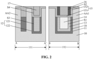
- FIG. 2 schematically shows a cross-sectional diagram of a structure along the lines A-A', B-B' of FIG. 1 .
- the semiconductor structure provided by the embodiments of the disclosure will be described further below with reference to the accompanying FIG. 1 to FIG. 2 .
- the semiconductor structure includes a substrate 10, a first isolation trench 11 located in the substrate 10, a first insulating layer 13 covering a bottom surface and a lower part of a sidewall of the first isolation trench 11, a second insulating layer 16 covering an upper part of the sidewall of the first isolation trench 11, and a third insulating layer 15 at least partially located between the first insulating layer 13 and the second insulating layer 16 to isolate the first insulating layer 13 and the second insulating layer 16.
- the semiconductor structure provided by the embodiments of the present disclosure may be a three-dimensional dynamic random access memory (3D DRAM), but is not limited thereto.
- the semiconductor structure may also be any semiconductor structure.
- the substrate may be a semiconductor substrate and may include at least one elemental semiconductor material, such as silicon (Si) substrate, germanium (Ge) substrate), at least one III-V compound semiconductor material, at least one II-VI compound semiconductor material, at least one organic semiconductor material, or other semiconductor materials known in the art.
- a semiconductor substrate is a silicon substrate, which may or may not be doped.
- the substrate 10 includes a device unit region 101, and a device core region or a peripheral region 102.
- the first isolation trench 11 is located in a device core region or a peripheral region 102 for isolating selection transistors.
- the first isolation trench 11 defines at least one first active area AA1 in the device core region or peripheral region 102.
- a selection transistor having a planar gate structure such as a P-type transistor or an N-type transistor may be formed on the first active area AA1.
- materials of the first insulating layer 13 and the second insulating layer 16 include nitride.
- nitride is used as the materials of the first insulating layer 13 and the second insulating layer 16.
- the material of the first insulating layer 13 may be the same as or be different from that of the second insulating layer 16.
- the material of the first insulating layer 13 is the same as that of the second insulating layer 16 for example, being silicon nitride. But it is not limited to the above, any material satisfying the stress requirements described above may be used as the materials of the first insulating layer 13 and the second insulating layer 16.
- the material of the third insulating layer 15 includes oxide, for example, silicon oxide.
- the first insulating layer 13 and the second insulating layer 16 have an ability to capture hot electrons.
- the third insulating layer 15 is used to isolate the first insulating layer 13 from the second insulating layer 16, thereby isolating hot electrons trapped in the first insulating layer 13 from hot electrons trapped in the second insulating layer 16, preventing the hot electrons trapped in the second insulating layer 16 from flowing to the first insulating layer 13, and thus reducing the number of the hot electrons stored in the first insulating layer 13. Meanwhile, the first insulating layer 13 and the second insulating layer 16 are isolated from each other.
- first insulating layer 13 and the second insulating layer 16 are not isolated from each other, carriers for storing hot electrons are reduced in the first insulating layer 13 and the second insulating layer 16, so that they only can store relatively few hot electrons, which can effectively alleviate the HEIP effect.
- a ratio of a height of the first insulating layer 13 to a height of the second insulating layer 16 should not be too large or too small.
- the ratio of the height of the first insulating layer 13 to the height of the second insulating layer 16 is too large, the first insulating layer 13 will extend to the upper part of the first isolation trench 11, and thus more hot electrons will be stored in the first insulating layer 13, and more holes will be accumulated in the upper part of the first active area AA1, which cannot effectively alleviate the HEIP effect.
- the ratio of the height of the first insulating layer 13 to the height of the second insulating layer 16 is too small, the height of the second insulating layer 16 located in the upper part of the first isolation trench 11 will be high, the second insulating layer 16 will capture a larger number of hot electrons, and thus more holes will be accumulated the upper part of the first active area AA1, which cannot effectively alleviate the HEIP effect, either.
- the ratio of the height of the first insulating layer 13 to the height of the second insulating layer 16 is in a range of 2 to 6, specifically, for example, 3, 4, 5, etc.
- a height of a part of the third insulating layer 15 located between the first insulating layer 13 and the second insulating layer 16 should not be too large or too small.
- the height of the part of the third insulating layer 15 located between the first insulating layer 13 and the second insulating layer 16 is too large, a sum of the height of the first insulating layer 13 and the height of the second insulating layer 16 will be too small, which results in that the first insulating layer 13 and the second insulating layer 16 cannot effectively raise the stress of the substrate 10.
- the height of the part of the third insulating layer 15 located between the first insulating layer 13 and the second insulating layer 16 is too small, the HEIP effect cannot be effectively alleviated.
- a ratio of the height of the part of the third insulating layer 15 located between the first insulating layer 13 and the second insulating layer 16 to the height of the second insulating layer 16 is in a range of 0.3 to 0.7, specifically, for example, 0.4, 0.5, 0.6, etc.
- both a thickness of the first insulating layer 13 and a thickness of the second insulating layer 16 are in a range of 5 nm to 30 nm. In some embodiments, both the thickness of the first insulating layer 13 and the thickness of the second insulating layer 16 are in range of 10 nm to 25 nm. In a specific embodiment, the thickness of the first insulating layer 13 is greater than that of the second insulating layer 16, and the second insulating layer 16 has a thinner thickness. Therefore, hot electrons stored in the first insulating layer 13 are relatively few, thereby effectively alleviating the HEIP effect.
- the semiconductor structure further includes: a fourth insulating layer 18 and a first filling layer 14.
- the fourth insulating layer 18 is located between the inner wall of the first isolation trench 11 and the first insulating layer 13, covers the bottom surface and the lower part of the sidewall of the first isolation trench 11.
- the first filling layer 14 fills a recess S1 defined by the first insulating layer 13 in the first isolation trench 11.
- a material of the fourth insulating layer 18 may be the same as that of the third insulating layer 15, for example, silicon oxide.
- a material of the first filling layers 14 may be an oxide, such as silicon oxide.
- the third insulating layer 15 includes a bottom layer 151 and a sidewall layer 152.
- the bottom layer 151 overs tops of the fourth insulating layer 18, the first insulating layer 13 and the first filling layer 14.
- the sidewall layer 152 is located between the upper part of the sidewall of the first isolation trench 11 and the second insulating layer 16.
- the third insulating layer 15 also covers the upper surface of the substrate 10.
- the substrate 10 is isolated from the first insulating layer 13 and the second insulating layer 16, thereby further alleviating the HEIP effect.
- the HEIP effect is effectively alleviated. Therefore, there is no need to additionally thicken the thicknesses of the fourth insulating layer 18 and the third insulating layer 15, which simplifies the process and increases processing windows.
- the semiconductor structure further includes a second filling layer 17.
- the second filling layer 17 fills a recess S2 defined by the second insulating layer 16 together with the bottom layer 151 of the third insulating layer 15 in the first isolation trench 11.
- a material of the second filling layer 17 may be the same as that of the first filling layer 14, for example, silicon oxide.
- the semiconductor structure further includes a second isolation trench 12.
- the second isolation trench 12 includes a first sub-trench 121 and a second sub-trench 122.
- a width of the second sub-trench 122 is greater than a width of the first sub-trench 121.
- second isolation trenches 12 are located in the device unit region 101 for isolating memory units, and define multiple second active areas AA2 arranged in parallel with each other in the device unit region 101.
- the first isolation trench 11 and the second isolation trench 12 are formed in the same processing operation, and the width of the first isolation trench 11 is greater than that of the first sub-trench 121 and that of the second sub-trenches 122.
- the fourth insulating layer 18 covers a bottom surface and a lower part of a sidewall of the second sub-trench 122.
- the first insulating layer 13 fills a recess S3 defined by the fourth insulating layer 18 in the second sub-trench 122.
- the third insulating layer 15 covers an upper part of a sidewall of the second sub-trench 122 and the tops of the fourth insulating layer 18 and the first insulating layer 13.
- the second filling layer 17 fills a recess S4 defined by the third insulating layer 15 in the second sub-trench 122.
- the fourth insulating layer 18 fills a lower part of the first sub-trench 121
- the third insulating layer 15 fills an upper part of the first sub-trench 121.
- the embodiments of the disclosure also provide a method for manufacturing a semiconductor structure, as shown in FIG. 3 .
- the method includes the following operations.
- a substrate is provided.
- the substrate is etched to form a first isolation trench.
- a first insulating layer is formed, and covers a bottom surface and a lower part of a sidewall of the first isolation trench.
- a third insulating layer is formed on the first insulating layer, at least covers a top of the first insulating layer.
- a second insulating layer is formed on the third insulating layer, covers an upper part of the sidewall of the first isolation trench, and is isolated from the first insulating layer by the third insulating layer.
- FIGS. 4 to 12 schematically show cross-sectional structures along lines A-A 'and B-B' of FIG. 1 during each processing operation.
- step S301 is performed and a substrate is provided.
- the substrate may be a semiconductor substrate and may include at least one elemental semiconductor material (such as silicon (Si) substrate, germanium (Ge) substrate), at least one III-V compound semiconductor material, at least one II-VI compound semiconductor material, at least one organic semiconductor material, or other semiconductor materials known in the art.
- a semiconductor substrate is a silicon substrate, which may or may not be doped.
- the substrate 10 includes a device unit region 101, and a device core region or a peripheral region 102.
- memory units may be formed in the device unit region 101 and selection transistors may be formed in the device core region or peripheral region 102.
- step S302 is performed, as shown in FIG. 5 , the substrate 10 is etched to form the first isolation trench 11.
- the first isolation trench 11 may be formed by photolithography and dry/wet etching processes.
- the first isolation trench 11 is formed in the device core or peripheral region 102, and defines at least one first active area AA1 in the device core region or peripheral region 102.
- a selection transistor having a planar gate structure such as a P-type transistor or an N-type transistor may be formed in the first active area AA1.
- the method further includes the following operations.
- the substrate 10 is etched to form to form a second isolation trench 12.
- the second isolation trench 12 includes a first sub-trench 121 and a second sub-trench 122.
- a width of the second sub-trench 122 is greater than a width of the first sub-trench 121.
- second isolation trenches 12 are formed in the device unit region 101 for isolating memory units, and define multiple second active areas AA2 arranged in parallel with each other in the device unit region 101.
- the memory units may subsequently be formed in the second active areas AA2 and the second isolation trenches 12 are used to isolate the memory units.
- the first isolation trenches 11 and the second isolation trenches 12 are formed in the same processing operation, thereby omitting one masking process, and thus simplifying the process.
- the width of the first isolation trenches 11 is greater than that of the first sub-trench 121 and that of the second sub-trench 122. It is to be understood that, since both the width of the first isolation trench 11 and that of the second sub-trench 122 are greater than the width of the first sub-trench 121, depths of the first isolation trench 11 and the second sub-trench 122 are greater than a depth of the first sub-trench 121 under the same etching conditions.
- step S303 is performed, and as shown in FIGS. 7 to 8 , a first insulating layer 13 is formed.
- the first insulating layer 13 covers a bottom surface and a lower part of the sidewall of the first isolation trench 11.
- a fourth insulating material layer 18' is formed before forming the first insulating layer 13.
- the fourth insulating material layer 18' covers inner surfaces of the first isolation trench 11 and the second sub-trench 122, and fills the first sub-trench 121.
- the fourth insulating material layer 18' also covers the upper surface of the substrate 10. It is to be understood that, since the depth and the width of the first sub-trench 121 are relative small, the fourth insulating material layer 18' can fully fill the first sub-trench 121, but cannot fully fill the first isolation trench 11 and the second sub-trench 122 under the same deposition conditions.
- the fourth insulating layer 18 finally formed fills a lower part of the first sub-trench 121.
- the fourth insulating material layer 18' may be formed by using an atomic layer deposition (ALD) process combined with an in-situ steam generation process (ISSG).
- a material of the fourth insulating layer 18 includes oxide, for example, silicon oxide.
- the forming the first insulating layer 13 includes the following operations.
- a first insulating material layer 13' is formed, covers the fourth insulating material layer 18', and fully fills the second sub-trench 122.
- a first filling material layer 14' is formed, covers the first insulating material layer 13', and fully fills the first isolation trench 11.
- the first filling material layer 14', the first insulating material layer 13' and the fourth insulating material layer 18' are etched to make tops of the first insulating material layer 13', the fourth insulating material layer 18' and the first filling material layer 14' lower than the upper surface of the substrate 10, thereby forming the first insulating layer 13, the fourth insulating layer 18 and the first filling layer 14.
- the first insulating material layer 13' and the first filling material layer 14' may be formed by using a chemical vapor deposition (CVD) process, a plasma enhanced chemical vapor deposition (PECVD) process, an atomic layer deposition (ALD) process, or a combination thereof.
- a material of the first insulating layer 13 includes nitride, for example, silicon nitride.
- a material of the first insulating layer 14 includes oxide, for example, silicon oxide.
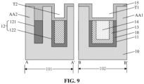
- step S304 is performed, and as shown in FIG. 9 , a third insulating layer 15 is formed on the first insulating layer 13.
- the third insulating layer 15 at least covers a top of the first insulating layer 13.
- the forming the third insulating layer 15 includes the following operations.
- a third insulating material layer (not shown in the figures) is formed and etched to form the third insulating layer 15 covering tops of the fourth insulating layer 18, the first insulating layer 13 and the first filling layer 14 and upper parts of sidewalls of the first isolation trench 11 and the second sub-trench 122.
- a part of the third insulating layer 15 within the first isolation trench 11 defines a first accommodating cavity T1
- a part of the third insulating layer 15 within the second sub-trench 122 defines a second accommodating cavity T2.
- the third insulating layer 15 also covers the upper surface of the substrate 10.
- the width and depth of the first sub-trench 121 are relative small, so that the third insulating layer 15 can fully fill a part of the first sub-trench 121 that is not filled by the fourth insulating layer 18 under the same deposition conditions.
- the third insulating layer 15 may be formed by using a chemical vapor deposition (CVD) process, a plasma enhanced chemical vapor deposition (PECVD) process, an atomic layer deposition (ALD) process, or a combination thereof.
- a material of the third insulating layer 15 includes oxide, for example, silicon oxide.
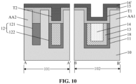
- step S305 is preformed, and as shown in FIGS. 10 to 11 , a second insulating layer 16 is formed over the third insulating layer 15.
- the second insulating layer 16 covers the upper part of the sidewall of the first isolation trench 11.
- the third insulating layer 15 isolates the first insulating layer 13 from the second insulating layer 16.
- the forming the second insulating layer 16 includes the following operations.
- a second insulating material layer 16' is formed, covers a bottom surface and a sidewall of the first accommodating cavity T1, and fully fills the second accommodating cavity T2.
- the second insulating material layer 16' is etched to removing the second insulating material layer 16' located in the second accommodating cavity T2 and the second insulating material layer 16' covering the bottom surface of the first accommodating cavity T1 to form the second insulating layer 16 covering the sidewall of the first accommodating cavity T1.
- the second insulating material layer 16' can fully fill the second accommodating cavity T2, but cannot fully fill the first accommodating cavity T1, under the same deposition conditions.
- the second insulating material layer 16 may be formed by using a chemical vapor deposition (CVD) process, a plasma enhanced chemical vapor deposition (PECVD) process, an atomic layer deposition (ALD) process, or a combination thereof.
- a material of the second insulating layer 16 includes nitride.
- nitride is used as the materials of the first insulating layer 13 and the second insulating layer 16.
- the material of the first insulating layer 13 may be the same as or be different from that of the second insulating layer 16.
- the material of the first insulating layer 13 is the same as that of the second insulating layer 16 for example, being silicon nitride. But it is not limited to the above, any material satisfying the stress requirements described above may be used as the materials of the first insulating layer 13 and the second insulating layer 16.
- the first insulating layer 13 and the second insulating layer 16 have an ability to capture hot electrons.
- the third insulating layer 15 is used to isolate the first insulating layer 13 from the second insulating layer 16, thereby isolating hot electrons trapped in the first insulating layer 13 from hot electrons trapped in the second insulating layer 16.
- the hot electrons in the second insulating layer 16 may be lost, and the presence of the third insulating layer 15 can prevent the hot electrons captured in the second insulating layer 16 from flowing into the first insulating layer 13. By doing so, the number of the hot electrons stored in the first insulating layer 13 can be reduced.
- the first insulating layer 13 and the second insulating layer 16 are isolated from each other. Compared with the case where the first insulating layer 13 and the second insulating layer 16 are not isolated from each other, carriers for storing hot electrons are reduced in the first insulating layer 13 and the second insulating layer 16, so that they only can store relatively few hot electrons, which can effectively alleviate the HEIP effect.
- a ratio of a height of the first insulating layer 13 to a height of the second insulating layer 16 should not be too large or too small.
- the ratio of the height of the first insulating layer 13 to the height of the second insulating layer 16 is too large, the first insulating layer 13 will extend to the upper part of the first isolation trench 11, and thus more hot electrons will be stored in the first insulating layer 13, and more holes will be accumulated in the upper part of the first active area AA1, which cannot effectively alleviate the HEIP effect.
- the ratio of the height of the first insulating layer 13 to the height of the second insulating layer 16 is too small, the height of the second insulating layer 16 located in the upper part of the first isolation trench 11 will be high, the second insulating layer 16 will capture a larger number of hot electrons, and thus more holes will be accumulated in the upper part of the first active area AA1, which cannot effectively alleviate the HEIP effect, either.
- the ratio of the height of the first insulating layer 13 to the height of the second insulating layer 16 is in a range of 2 to 6, specifically, for example, 3, 4, 5, etc.
- a height of a part of the third insulating layer 15 located between the first insulating layer 13 and the second insulating layer 16 should not be too large or too small.
- the height of the part of the third insulating layer 15 between the first insulating layer 13 and the second insulating layer 16 is too large, a sum of the height of the first insulating layer 13 and the height of the second insulating layer 16 will be too small, which results in that the first insulating layer 13 and the second insulating layer 16 cannot effectively raise the stress of the substrate 10.
- the height of the part of the third insulating layer 15 located between the first insulating layer 13 and the second insulating layer 16 is too small, the HEIP effect cannot be effectively alleviated.
- a ratio of the height of the part of the third insulating layer 15 located between the first insulating layer 13 and the second insulating layer 16 to the height of the second insulating layer 16 is in a range of 0.3 to 0.7, specifically, for example, 0.4, 0.5, 0.6, etc.
- both a thickness of the first insulating layer 13 and a thickness of the second insulating layer 16 are in a range of 5 nm to 30 nm. In some embodiments, both the thickness of the first insulating layer 13 and the thickness of the second insulating layer 16 are in a range of 10 nm to 25 nm. In a specific embodiment, the thickness of the first insulating layer 13 is greater than that of the second insulating layer 16, and the second insulating layer 16 has a thinner thickness. Therefore, hot electrons stored in the first insulating layer 13 are relatively few, thereby effectively alleviating the HEIP effect.
- the fourth insulating layer 18 and the third insulating layer 15 isolate the substrate 10 from the first insulating layer 13 and the second insulating layer 16, respectively, thereby further alleviating the HEIP effect.
- the HEIP effect is effectively alleviated. Therefore, there is no need to additionally thicken the thicknesses of the fourth insulating layer 18 and the third insulating layer 15, which simplifies the process and increases processing windows.
- the method further includes the following operations.
- a second filling material layer 17' is formed on the third insulating layer 15 and the second insulating layer 16. The second filling material layer 17' fully fills the first accommodating cavity T1 and second accommodating cavity T2.
- the second filling material layer 17' is etched to make a top of the second filling material layer 17' flush with a top of the second insulating layer 16, thereby forming a second filling layer 17.
- the third insulating layer is used to isolate the first insulating layer from the second insulating layer, thereby isolating hot electrons trapped in the first insulating layer from hot electrons trapped in the second insulating layer, preventing the hot electrons trapped in the second insulating layer from flowing to the first insulating layer, and thus reducing the number of the hot electrons stored in the first insulating layer. Meanwhile, the first insulating layer and the second insulating layer are isolated from each other.
Landscapes
- Engineering & Computer Science (AREA)
- Manufacturing & Machinery (AREA)
- Element Separation (AREA)
- Semiconductor Memories (AREA)
- Insulated Gate Type Field-Effect Transistor (AREA)
- Thin Film Transistor (AREA)
Applications Claiming Priority (2)
| Application Number | Priority Date | Filing Date | Title |
|---|---|---|---|
| CN202210726332.2A CN117316975A (zh) | 2022-06-23 | 2022-06-23 | 一种半导体结构及其制造方法 |
| PCT/CN2022/105152 WO2023245760A1 (fr) | 2022-06-23 | 2022-07-12 | Structure semi-conductrice et procédé de fabrication correspondant |
Publications (2)
| Publication Number | Publication Date |
|---|---|
| EP4318558A1 true EP4318558A1 (fr) | 2024-02-07 |
| EP4318558A4 EP4318558A4 (fr) | 2025-03-19 |
Family
ID=86661471
Family Applications (1)
| Application Number | Title | Priority Date | Filing Date |
|---|---|---|---|
| EP22769874.3A Pending EP4318558A4 (fr) | 2022-06-23 | 2022-07-12 | Structure semi-conductrice et procédé de fabrication correspondant |
Country Status (7)
| Country | Link |
|---|---|
| US (1) | US12419043B2 (fr) |
| EP (1) | EP4318558A4 (fr) |
| JP (1) | JP7588153B2 (fr) |
| KR (1) | KR102838911B1 (fr) |
| CN (1) | CN117316975A (fr) |
| TW (1) | TWI839889B (fr) |
| WO (1) | WO2023245760A1 (fr) |
Families Citing this family (1)
| Publication number | Priority date | Publication date | Assignee | Title |
|---|---|---|---|---|
| CN119255595B (zh) * | 2023-06-25 | 2025-10-03 | 长鑫存储技术有限公司 | 半导体结构及其形成方法 |
Family Cites Families (21)
| Publication number | Priority date | Publication date | Assignee | Title |
|---|---|---|---|---|
| DE10348021A1 (de) * | 2003-10-15 | 2005-05-25 | Infineon Technologies Ag | Verfahren zur Herstellung einer Halbleiterstruktur mit einer Einkapselung einer Füllung, welche zum Anfüllen von Gräben verwendet wird |
| KR100746223B1 (ko) * | 2005-09-09 | 2007-08-03 | 삼성전자주식회사 | 반도체소자의 트렌치 소자분리 방법 |
| KR100801733B1 (ko) * | 2005-12-29 | 2008-02-11 | 주식회사 하이닉스반도체 | 서로 다른 두께의 측벽산화막을 갖는 트랜치 소자분리막형성방법 |
| KR100972681B1 (ko) | 2007-05-11 | 2010-07-27 | 주식회사 하이닉스반도체 | 플래시 메모리 소자의 소자 분리막 형성 방법 |
| KR20080114065A (ko) * | 2007-06-26 | 2008-12-31 | 주식회사 하이닉스반도체 | 반도체 소자의 소자분리막 형성 방법 |
| KR100984859B1 (ko) * | 2008-04-29 | 2010-10-04 | 주식회사 하이닉스반도체 | 반도체 소자의 소자분리막 및 그 형성방법 |
| KR100972899B1 (ko) * | 2008-07-25 | 2010-07-28 | 주식회사 하이닉스반도체 | 반도체 소자의 제조방법 |
| JP2010080498A (ja) * | 2008-09-24 | 2010-04-08 | Toshiba Corp | 不揮発性半導体記憶装置およびその製造方法 |
| US8367515B2 (en) * | 2008-10-06 | 2013-02-05 | Taiwan Semiconductor Manufacturing Company, Ltd. | Hybrid shallow trench isolation for high-k metal gate device improvement |
| KR100997796B1 (ko) * | 2008-12-16 | 2010-12-02 | 주식회사 하이닉스반도체 | 반도체 소자의 제조방법 |
| KR101069438B1 (ko) * | 2009-09-14 | 2011-09-30 | 주식회사 하이닉스반도체 | 반도체 소자의 소자분리막 형성방법 |
| KR101062849B1 (ko) * | 2009-10-30 | 2011-09-07 | 주식회사 하이닉스반도체 | 반도체 장치 및 그 제조 방법 |
| KR20120091567A (ko) | 2011-02-09 | 2012-08-20 | 삼성전자주식회사 | 소자 분리막 구조물 형성 방법 |
| US8399363B1 (en) * | 2011-02-28 | 2013-03-19 | Samsung Electronics Co., Ltd. | Methods of forming oxide-filled trenches in substrates using multiple-temperature oxide deposition techniques |
| CN103811543B (zh) * | 2012-11-05 | 2018-09-18 | 中国科学院微电子研究所 | 半导体器件及其制造方法 |
| CN106531680A (zh) * | 2015-09-09 | 2017-03-22 | 旺宏电子股份有限公司 | 隔离结构及其制造方法 |
| KR20180068229A (ko) * | 2016-12-13 | 2018-06-21 | 삼성전자주식회사 | 반도체 장치 및 이의 제조 방법 |
| KR102459430B1 (ko) | 2018-01-08 | 2022-10-27 | 삼성전자주식회사 | 반도체 소자 및 그 제조방법 |
| KR102733882B1 (ko) | 2018-09-05 | 2024-11-26 | 삼성전자주식회사 | 소자분리층을 갖는 반도체 소자 및 그 제조 방법 |
| KR102815971B1 (ko) | 2020-08-14 | 2025-06-04 | 에스케이하이닉스 주식회사 | 반도체장치 및 그 제조 방법 |
| KR102845501B1 (ko) | 2020-12-07 | 2025-08-12 | 삼성전자주식회사 | 반도체 소자 |
-
2022
- 2022-06-23 CN CN202210726332.2A patent/CN117316975A/zh active Pending
- 2022-07-12 KR KR1020227031206A patent/KR102838911B1/ko active Active
- 2022-07-12 EP EP22769874.3A patent/EP4318558A4/fr active Pending
- 2022-07-12 WO PCT/CN2022/105152 patent/WO2023245760A1/fr not_active Ceased
- 2022-07-12 JP JP2022562320A patent/JP7588153B2/ja active Active
- 2022-09-20 US US17/948,918 patent/US12419043B2/en active Active
- 2022-10-12 TW TW111138639A patent/TWI839889B/zh active
Also Published As
| Publication number | Publication date |
|---|---|
| US20230017189A1 (en) | 2023-01-19 |
| EP4318558A4 (fr) | 2025-03-19 |
| KR102838911B1 (ko) | 2025-07-24 |
| KR20220130244A (ko) | 2022-09-26 |
| JP7588153B2 (ja) | 2024-11-21 |
| JP2024527641A (ja) | 2024-07-26 |
| TW202306119A (zh) | 2023-02-01 |
| CN117316975A (zh) | 2023-12-29 |
| US12419043B2 (en) | 2025-09-16 |
| WO2023245760A1 (fr) | 2023-12-28 |
| TWI839889B (zh) | 2024-04-21 |
Similar Documents
| Publication | Publication Date | Title |
|---|---|---|
| US12033898B2 (en) | Method of fabricating a FinFET device | |
| US20230343787A1 (en) | Semiconductor device | |
| JP6338631B2 (ja) | スプリットゲートフラッシュ技術におけるインターディジテートキャパシタ | |
| CN109980012A (zh) | 半导体器件 | |
| CN106941120A (zh) | 具有掩埋栅结构的半导体器件及其制造方法以及存储单元 | |
| KR20160059862A (ko) | 반도체 장치 및 그 제조 방법 | |
| US12324188B2 (en) | Field effect transistor with source/drain contact isolation structure and method | |
| TW202131389A (zh) | 半導體結構及其形成方法 | |
| US9691867B2 (en) | Semiconductor device including spacers having different dimensions | |
| TW201909282A (zh) | 半導體裝置及其製程 | |
| CN109560080A (zh) | 半导体器件 | |
| US20190311906A1 (en) | Semiconductor structure with metal gate, and method for manufacturing the same | |
| EP4318558A1 (fr) | Structure semi-conductrice et procédé de fabrication correspondant | |
| US20240194756A1 (en) | Vertical self aligned gate all around transistor | |
| JP2014143269A (ja) | 半導体装置の製造方法 | |
| US12268029B2 (en) | Method for manufacturing semiconductor device | |
| CN114267640A (zh) | 半导体器件及其制备方法 | |
| CN107644815A (zh) | 一种半导体器件及其制造方法和电子装置 | |
| CN114188413B (zh) | 半导体结构及其形成方法 | |
| CN119421417B (zh) | 半导体结构及其制备方法 | |
| CN119421418B (zh) | 半导体结构及其制备方法 | |
| CN118714844B (zh) | 半导体结构及其制备方法 | |
| US20240332400A1 (en) | Semiconductor structure and forming method thereof | |
| KR20240165894A (ko) | 반도체 소자 및 그의 제조 방법 | |
| CN117913122A (zh) | 一种半导体器件及其制造方法 |
Legal Events
| Date | Code | Title | Description |
|---|---|---|---|
| STAA | Information on the status of an ep patent application or granted ep patent |
Free format text: STATUS: UNKNOWN |
|
| STAA | Information on the status of an ep patent application or granted ep patent |
Free format text: STATUS: THE INTERNATIONAL PUBLICATION HAS BEEN MADE |
|
| PUAI | Public reference made under article 153(3) epc to a published international application that has entered the european phase |
Free format text: ORIGINAL CODE: 0009012 |
|
| STAA | Information on the status of an ep patent application or granted ep patent |
Free format text: STATUS: REQUEST FOR EXAMINATION WAS MADE |
|
| 17P | Request for examination filed |
Effective date: 20220923 |
|
| AK | Designated contracting states |
Kind code of ref document: A1 Designated state(s): AL AT BE BG CH CY CZ DE DK EE ES FI FR GB GR HR HU IE IS IT LI LT LU LV MC MK MT NL NO PL PT RO RS SE SI SK SM TR |
|
| A4 | Supplementary search report drawn up and despatched |
Effective date: 20250217 |
|
| RIC1 | Information provided on ipc code assigned before grant |
Ipc: H01L 21/762 20060101AFI20250211BHEP |
|
| DAV | Request for validation of the european patent (deleted) | ||
| DAX | Request for extension of the european patent (deleted) |