EP4318903A1 - Digital gesteuerter gleichspannungswandler - Google Patents
Digital gesteuerter gleichspannungswandler Download PDFInfo
- Publication number
- EP4318903A1 EP4318903A1 EP22306168.0A EP22306168A EP4318903A1 EP 4318903 A1 EP4318903 A1 EP 4318903A1 EP 22306168 A EP22306168 A EP 22306168A EP 4318903 A1 EP4318903 A1 EP 4318903A1
- Authority
- EP
- European Patent Office
- Prior art keywords
- voltage
- converter
- signal
- coupled
- input
- Prior art date
- Legal status (The legal status is an assumption and is not a legal conclusion. Google has not performed a legal analysis and makes no representation as to the accuracy of the status listed.)
- Pending
Links
Images


Classifications
-
- H—ELECTRICITY
- H02—GENERATION; CONVERSION OR DISTRIBUTION OF ELECTRIC POWER
- H02M—APPARATUS FOR CONVERSION BETWEEN AC AND AC, BETWEEN AC AND DC, OR BETWEEN DC AND DC, AND FOR USE WITH MAINS OR SIMILAR POWER SUPPLY SYSTEMS; CONVERSION OF DC OR AC INPUT POWER INTO SURGE OUTPUT POWER; CONTROL OR REGULATION THEREOF
- H02M3/00—Conversion of DC power input into DC power output
- H02M3/02—Conversion of DC power input into DC power output without intermediate conversion into AC
- H02M3/04—Conversion of DC power input into DC power output without intermediate conversion into AC by static converters
- H02M3/10—Conversion of DC power input into DC power output without intermediate conversion into AC by static converters using discharge tubes with control electrode or semiconductor devices with control electrode
- H02M3/145—Conversion of DC power input into DC power output without intermediate conversion into AC by static converters using discharge tubes with control electrode or semiconductor devices with control electrode using devices of a triode or transistor type requiring continuous application of a control signal
- H02M3/155—Conversion of DC power input into DC power output without intermediate conversion into AC by static converters using discharge tubes with control electrode or semiconductor devices with control electrode using devices of a triode or transistor type requiring continuous application of a control signal using semiconductor devices only
- H02M3/156—Conversion of DC power input into DC power output without intermediate conversion into AC by static converters using discharge tubes with control electrode or semiconductor devices with control electrode using devices of a triode or transistor type requiring continuous application of a control signal using semiconductor devices only with automatic control of output voltage or current, e.g. switching regulators
- H02M3/157—Conversion of DC power input into DC power output without intermediate conversion into AC by static converters using discharge tubes with control electrode or semiconductor devices with control electrode using devices of a triode or transistor type requiring continuous application of a control signal using semiconductor devices only with automatic control of output voltage or current, e.g. switching regulators with digital control
-
- H—ELECTRICITY
- H02—GENERATION; CONVERSION OR DISTRIBUTION OF ELECTRIC POWER
- H02M—APPARATUS FOR CONVERSION BETWEEN AC AND AC, BETWEEN AC AND DC, OR BETWEEN DC AND DC, AND FOR USE WITH MAINS OR SIMILAR POWER SUPPLY SYSTEMS; CONVERSION OF DC OR AC INPUT POWER INTO SURGE OUTPUT POWER; CONTROL OR REGULATION THEREOF
- H02M1/00—Details of apparatus for conversion
- H02M1/0003—Details of control, feedback or regulation circuits
- H02M1/0012—Control circuits using digital or numerical techniques
-
- H—ELECTRICITY
- H02—GENERATION; CONVERSION OR DISTRIBUTION OF ELECTRIC POWER
- H02M—APPARATUS FOR CONVERSION BETWEEN AC AND AC, BETWEEN AC AND DC, OR BETWEEN DC AND DC, AND FOR USE WITH MAINS OR SIMILAR POWER SUPPLY SYSTEMS; CONVERSION OF DC OR AC INPUT POWER INTO SURGE OUTPUT POWER; CONTROL OR REGULATION THEREOF
- H02M1/00—Details of apparatus for conversion
- H02M1/0003—Details of control, feedback or regulation circuits
- H02M1/0025—Arrangements for modifying reference values, feedback values or error values in the control loop of a converter
-
- H—ELECTRICITY
- H02—GENERATION; CONVERSION OR DISTRIBUTION OF ELECTRIC POWER
- H02M—APPARATUS FOR CONVERSION BETWEEN AC AND AC, BETWEEN AC AND DC, OR BETWEEN DC AND DC, AND FOR USE WITH MAINS OR SIMILAR POWER SUPPLY SYSTEMS; CONVERSION OF DC OR AC INPUT POWER INTO SURGE OUTPUT POWER; CONTROL OR REGULATION THEREOF
- H02M1/00—Details of apparatus for conversion
- H02M1/08—Circuits specially adapted for the generation of control voltages for semiconductor devices incorporated in static converters
- H02M1/088—Circuits specially adapted for the generation of control voltages for semiconductor devices incorporated in static converters for the simultaneous control of series or parallel connected semiconductor devices
-
- H—ELECTRICITY
- H02—GENERATION; CONVERSION OR DISTRIBUTION OF ELECTRIC POWER
- H02M—APPARATUS FOR CONVERSION BETWEEN AC AND AC, BETWEEN AC AND DC, OR BETWEEN DC AND DC, AND FOR USE WITH MAINS OR SIMILAR POWER SUPPLY SYSTEMS; CONVERSION OF DC OR AC INPUT POWER INTO SURGE OUTPUT POWER; CONTROL OR REGULATION THEREOF
- H02M3/00—Conversion of DC power input into DC power output
- H02M3/02—Conversion of DC power input into DC power output without intermediate conversion into AC
- H02M3/04—Conversion of DC power input into DC power output without intermediate conversion into AC by static converters
- H02M3/10—Conversion of DC power input into DC power output without intermediate conversion into AC by static converters using discharge tubes with control electrode or semiconductor devices with control electrode
- H02M3/145—Conversion of DC power input into DC power output without intermediate conversion into AC by static converters using discharge tubes with control electrode or semiconductor devices with control electrode using devices of a triode or transistor type requiring continuous application of a control signal
- H02M3/155—Conversion of DC power input into DC power output without intermediate conversion into AC by static converters using discharge tubes with control electrode or semiconductor devices with control electrode using devices of a triode or transistor type requiring continuous application of a control signal using semiconductor devices only
- H02M3/156—Conversion of DC power input into DC power output without intermediate conversion into AC by static converters using discharge tubes with control electrode or semiconductor devices with control electrode using devices of a triode or transistor type requiring continuous application of a control signal using semiconductor devices only with automatic control of output voltage or current, e.g. switching regulators
- H02M3/158—Conversion of DC power input into DC power output without intermediate conversion into AC by static converters using discharge tubes with control electrode or semiconductor devices with control electrode using devices of a triode or transistor type requiring continuous application of a control signal using semiconductor devices only with automatic control of output voltage or current, e.g. switching regulators including plural semiconductor devices as final control devices for a single load
Definitions
- a direct current (DC) to DC converter is in a common class of devices used widely to convert DC at one voltage to DC at another voltage.
- a DC-DC buck converter reduces the voltage at the output from the input voltage.
- a DC-DC converter always wastes some energy during the conversion. Reducing the loss is important for reducing general energy consumption and still more important for battery-powered devices in order to extend the battery life.
- many DC-DC converters are configured with switching power supplies. Two or more transistors between the input and the output voltage are switched on and off with some duty cycle to increase or decrease the voltage, respectively.
- a filter circuit is used at the output to reduce voltage ripples caused by the switching.
- the duty cycles of the switching transistors are regulated based on a desired reference voltage.
- Many DC-DC converters use a regulation loop with precision analog voltage regulation circuitry.
- the quality of the analog circuitry determines the accuracy of the output voltage, but quality analog circuitry is expensive and may be large. Deep stability analysis is used to develop the complex design of a quality analog regulation loop for a ramp generator, a current sensor for current mode, a transconductance cell and a loop comparator.
- ADC analog-to-digital converter
- the ADC allows the analog output voltage to be compared to a digital reference value.
- the accuracy of the analog output voltage depends on the quality of the ADC.
- a high quality accumulator and high bit count for the counter in the ADC is used. Accordingly, a high quality ADC may also be expensive and require a large area on an integrated circuit (IC).
- a digitally controlled DC-DC converter is described.
- a power stage is coupled to an input voltage and to a control signal and is configured to generate an output voltage in response to the control signal.
- a controller generates the control signal and is coupled to the power stage to provide the control signal to the power stage.
- the controller has an adjustment block coupled to the power stage output voltage to compare the output voltage to a reference voltage to generate a comparison signal, a logic circuit coupled to the adjustment block to receive the comparison signal and to generate the control signal in response to the comparison signal using a control word, and a digital-to analog converter coupled to the adjustment block, the power stage input voltage and the logic circuit to receive the control word from the logic circuit and to generate a converter voltage representing the control word using another voltage, the converter voltage being applied to the adjustment block to adjust the comparison signal.
- the another voltage is the input voltage to the power stage.
- the adjustment block includes an error amplifier coupled to the output voltage and to the reference voltage to generate an error voltage that represents a difference between the output voltage and the reference voltage, and a comparator coupled to the error amplifier and the logic circuit to receive the error voltage and the converter voltage and to generate the comparison signal in response to comparing the error voltage and the converter voltage.
- the another voltage is an error voltage related to a difference between the output voltage and the reference voltage.
- the adjustment block includes an error amplifier coupled to the output voltage and to the reference voltage to generate an error voltage that represents a difference between the output voltage and the reference voltage, and a comparator coupled to the error amplifier and the logic circuit to receive the input voltage and the converter voltage and to generate the comparison signal in response to comparing the input voltage and the converter voltage.
- control word represents a duty cycle of the control signal using a number of bits and wherein the converter voltage scales the another voltage based on the duty cycle. In some embodiments, the control word represents a ratio of the output voltage to the input voltage. In some embodiments, the logic circuit generates the control word using an up and down counter and wherein the up and down counter counts in response to the comparison signal.
- the logic circuit is coupled to a clock signal having a clock frequency and wherein the control signal is a pulse width modulation signal having a switching cycle determined by the clock frequency. In some embodiments, the logic circuit adjusts the control word at each switching cycle. In some embodiments, the logic circuit adjusts the control word by one bit at each switching cycle. In some embodiments, the logic circuit comprises a counter coupled to receive the comparison signal and to increment or decrement the control word based on the received comparison signal. In some embodiments, the power stage comprises switches between the input voltage and the output voltage and wherein the power stage opens and closes the switches in response to the control signal.
- the power stage switches are coupled in series with the control signal coupled to the gates of the switches and with the output voltage at a common drain of the switches.
- the power converter comprises a direct current to direct current buck converter.
- a method of operating a power converter comprising an input, an output, a controller, and a power stage coupled between the input and the output.
- the method includes receiving an input voltage at the power stage input, generating an output voltage at the power stage output in response to a control signal, comparing the output voltage to a reference voltage, generate a comparison signal in response to the comparing, generating the control signal in the controller in response to the comparison signal using a control word, and generating a converter voltage representing the control word in a digital-to-analog converter using another voltage, wherein the converter voltage is applied to adjust the comparison signal.
- generating a comparison signal includes generating an error voltage that represents a difference between the output voltage and the reference voltage, generating the converter voltage by factoring the input voltage by the control word, and generating the comparison signal in response to comparing the error voltage and the converter voltage.
- generating a comparison signal includes generating an error voltage that represents a difference between the output voltage and the reference voltage, generating the converter voltage by factoring the error voltage by the control word, and generating the comparison signal in response to comparing the converter voltage and the input voltage.
- Some embodiments further include generating the control word using an up and down counter, wherein the up and down counter counts in response to the comparison signal. Some embodiments further include a clock signal having a clock frequency and wherein generating the control signal comprises generating a pulse width modulation signal having a switching cycle determined by the clock frequency. In some embodiments, the power stage comprises switches between the input voltage and the output voltage and wherein generating the output voltage comprises opening and closing the switches in response to the control signal.
- a power converter includes means for generating an output voltage using an input voltage in response to a control signal, means for comparing the output voltage to a reference voltage and generating a comparison signal in response to the comparing, means for generating the control signal in response to the comparison signal using a control word, and means for converting the control word from digital to analog to generate the converter voltage wherein the converter voltage is applied to adjust the comparison signal.
- the means for comparing includes means for generating an error voltage that represents a difference between the output voltage and the reference voltage and means for generating the comparison signal in response to comparing the error voltage and the converter voltage, wherein the means for generating the converter voltage factors the input voltage by the control word.
- the means for comparing includes means for generating an error voltage that represents a difference between the output voltage and the reference voltage and means generating the comparison signal in response to comparing the converter voltage and the input voltage, wherein the means for generating the converter voltage factors the error voltage by the control word.
- the means for generating the control word comprises an up and down counter, wherein the up and down counter counts in response to the comparison signal.
- the means for generating the control signal generates a pulse width modulation signal having a switching cycle determined by an input clock frequency.
- the means for generating an output voltage opens and closes switches between the input voltage and the output voltage in response to the control signal.
- a DC-DC converter has a regulation loop that is both accurate and inexpensive.
- the power stage is coupled to a digital regulation loop that uses a digital-to-analog converter (DAC). No ADC is required.
- the controller uses an error amplifier, a comparator, and a digital block with the DAC.
- the regulation loop may be used with a buck converter, a boost converter, or derivatives, or combinations thereof.
- Embodiments are shown as single phase converters, although according to various other embodiments, different switch module converter topologies for the power stage may be used, for example a multiphase buck converter, or multiphase boost converter.
- the converter may be a single-transistor forward type converter, a two-transistor forward type converter, a push-pull type converter, a half bridge type converter or a full bridge type converter.
- the converters are used to drive a load that may be any electrical or electronic circuit requiring regulated power, such as computer equipment, telecommunications equipment, instrumentation, motors, etc.
- Fig. 1 is a circuit diagram of a DC-DC buck converter 100.
- the DC-DC buck converter 200 has a power stage 102 to reduce the input voltage to an output voltage, an output filter stage 104 to reduce ripples in the output voltage, and a control stage 106 to regulate the action of the power stage.
- the control stage is a digital regulation loop.
- the power stage has a P-type power metal oxide semiconductor field effect transistor (MOSFET) 124 and an N-type power MOSFET 126 connected anti-parallel and in series.
- the drain of the P-type power MOSFET 124 is coupled to the drain of the N-type power MOSFET 126 through a common drain node 128.
- the power stage is coupled to an input voltage, Vin, at an input node 122 and to a control signal, Vpwm, at a control node 130 and is configured to generate an output voltage, Vout, at an output terminal 146, in response to the control signal, Vpwm.
- the power stage receives the input DC voltage Vin across a positive node at the input node 122 and a common or ground node 123.
- the positive node 122 is coupled to a source of the P-type power MOSFET 124.
- the ground node is coupled to a source of the N-type power MOSFET 126.
- the P-type power MOSFET 124 and the N-type power MOSFET 126 are both regulated in common by the control voltage, Vpwm, provided to the control node 130.
- the control node is coupled to a gate 132 of the P-type MOSFET 124 and to a gate 134 of the N-type power MOSFET 126.
- the control voltage, Vpwm applies a pulse width modulation (PWM) signal to the control node 130 to control the reduction in voltage through the power stage 102.
- PWM pulse width modulation
- the power stage 102 may be simpler or more complex to suit different uses of the DC-DC buck converter 100.
- the output filter stage 104 has a series inductor 142 coupled to the common power node 128 of the power stage on one side and the output terminal 146 on the other side.
- a parallel capacitor 144 is coupled between the output terminal 146 and ground 148.
- the output voltage, Vout, with reduced power output power from the DC-DC buck converter 100 is taken across the output terminal 146 and ground 148 and is coupled to a load (not shown).
- the simple inductor-capacitor output filter is sufficient for many applications. Other types of components may be used to suit details of particular physical implementations. A simpler or more complex output filter stage may be used to suit different uses of the DC-DC buck converter 100.
- the control stage 106 has a controller 160 to generate the control signal, Vpwm, and is coupled to the power stage 102 to provide the control signal to the power stage.
- the controller is coupled to the output terminal 146 to receive the output voltage, Vout, at a first input terminal 162 of the controller 160.
- the controller 160 is coupled to the input node 122 to receive the input voltage, Vin, at a second input terminal 164.
- the controller compares the input voltage, Vin, to the output voltage, Vout, and regulates the power stage 102 using the control voltage, Vpwm, provided from the controller 160 to the control node 130 of the power stage 102.
- the controller 160 further receives a reference voltage selection signal, Vout sel, at a third input 166 and a clock signal, Clk, for example a stable reference clock at a fourth input terminal 168 to regulate operations within the controller 160.
- Fig. 2 is a block diagram of an example controller 200 suitable for use in a digital regulation loop for a DC-DC buck converter as described in Fig. 1 .
- the controller 160 includes an adjustment block 202 coupled to receive the output voltage, Vout, from the output terminal 146.
- the adjustment block 202 is also coupled reference source to receive a reference voltage selection signal, Vref_sel.
- the adjustment block compares the output voltage, Vout, to the reference voltage selection signal, Vref_sel, to generate a comparison signal, Comp.
- the controller 200 includes a logic circuit 204 coupled to the adjustment block 202 to receive the comparison signal, Comp, and to generate the control signal Vpwm, in response to the comparison using a control word, D.
- the control signal, Vpwm is coupled to the common control node 130 to regulate the power stage 102.
- the logic circuit 204 generates the control signal, Vpwm, using the control word, D, which is coupled to a DAC 206 of the controller.
- the DAC 206 receives the control word, D, and converts it to analog output as a converter voltage, Vdac, that is coupled as an input to the adjustment block 202.
- the DAC 206 is also coupled to the input voltage, Vin, to receive the input voltage.
- the DAC generates the converter voltage, Vdac, representing the control word, D, in analog form using the input voltage, Vin.
- the converter voltage, Vdac is applied to the adjustment block 202 to adjust the comparison signal, Comp.
- the adjustment block 202 includes an error amplifier 208 and a comparator 210.
- the error amplifier 208 is coupled to the output voltage, Vout, for example at the output terminal 146 and to the reference voltage selection signal, Vout_sel, to generate an error voltage, Vamp, that represents a difference between the output voltage, Vout, and the reference voltage selection signal, Vout_sel.
- the reference voltage selection signal, Vout_sel is described here as a constant, but may be varied over time to suit the load, for example for startup and shutdown operations or for high load and low load operations.
- the output voltage, Vout is scaled by a first series resistor, R1, at the error amplifier 208 input, and a second feedback resistor, R2, between the error voltage, Vamp, output and the output voltage, Vout, input to the error amplifier.
- the resistors adjust the gain of the output voltage, Vout, by a ratio R2/R1.
- the adjustment block 202 also includes a comparator 210 coupled to the error voltage, Vamp, which is the output of the error amplifier as an input and to the converter voltage, Vdac, as an input.
- the comparator 210 compares the error voltage, Vamp, and the converter voltage, Vdac, and generates the comparison signal, Comp, in response to comparing the error voltage, Vamp, and the converter voltage, Vdac.
- the comparison signal is provided to the logic circuit 204 to generate the control signal, Vpwm.
- Fig. 3 is a block diagram of an example logic circuit 300 suitable for use in the digital regulation loop of Fig. 2 .
- the logic circuit receives the comparison signal, Comp, as an input to a counter 322.
- a clock signal, Clk is provided to a clock divider 324.
- the clock divider 324 divides the input clock signal, Clk, by a number N.
- the divided clock signal, Clk_sw defines the switching frequency of the DC-DC buck converter.
- the counter counts up to N bits from 0 to 2 N .
- the counter 322 uses the divided clock signal, Clk_sw, from the clock divider 324 to increment or decrement its output, the control word, D, based on the input comparison signal, Comp.
- the control word, D is described as having N bits.
- the number of bits for the DAC is configured for the desired control voltage, Vpwm, accuracy which determines the output voltage accuracy.
- the number of bits may be configured by the clock frequency of the divided clock signal, Clk_sw, to the counter.
- the frequency of the clock signal, Clk, to the ramp generator 326 determines the number of bits in the ramp output to the ramp generator which controls the duty cycle of the power stage and therefore the times at which the power stage switches change state during the switching frequency of the DC-DC buck converter.
- the control word, D is an input to a comparator 328 to control the duty cycle of the logic circuit output voltage, the control voltage, Vpwm.
- An input ramp generator 326 receives the clock signal, Clk, and generates an N -bit ramp using the clock signal.
- the N -bit ramp is provided as a second input to the comparator 328.
- the compensation word, D is combined with the N -bit ramp in the comparator 328 to impose a duty cycle onto the N -bit ramp, as determined by the control word, D, to generate the control signal, Vpwm.
- the duty cycle of the control signal, Vpwm may be from 0% with a compensation word, D, of 0, to 100% with a compensation word of 2 N .
- N is 6, however, other values from 3 to 8 and beyond may be used.
- the control signal, Vpwm is provided from the comparator 328 to the output stage 102, as discussed above to control the duty cycle of the output stage 102 and thereby to control the output voltage, Vout, of the DC-DC buck converter.
- the duty cycle may be considered as the ratio of on time to off time of the power stage switches.
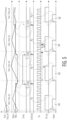
- Fig. 4 is a signal timing diagram of an example portion of the operation of the logic circuit 300 of the DC-DC buck converter 100 as described with respect to Fig. 3 .
- the signal state as high or low is shown on the vertical axis against time on the horizontal axis.
- the top signal is the clock signal, Clk, that is the input clock signal applied to the ramp generator 326.
- the divided clock signal, Clk_sw also updates the counter 322 of the logic circuit 300.
- the ramp is the N- bit ramp signal from the ramp generator 326.
- Comp is the comparison signal sent to the counter 322 as the input to the counter 322.
- Counter is an intermediate state within the counter 322 in which the control word, D, is incremented or decremented by a count of 1.
- Vpwm is the control signal generated by the ramp generator 328 by combining the control word, D, and the ramp.
- the divided clock signal, Clk_sw divides the clock signal, Clk, by 2 N , which is eight in this example.
- a single clock count is shown as having a short duration 402, 404, and eight clock counts are shown as defining a cycle 404, 406 of the logic circuit.
- the ramp signal increments from 0 to 7 and back to 0 in the time of each cycle. This corresponds to 8 bits per cycle and N is set to 3.
- the ramp is delayed by one count.
- the comparison signal, Comp is high at 410. This pushes the counter signal to increment by +1 at 412 for the duration of the cycle 404.
- the comparison signal, Comp is low at 416.
- the control signal, Vpwm has a duty cycle that may be changed with each cycle.
- the duty cycle is controlled by the ramp signal so that it may have a duty cycle or ON time of from 0-8 parts of a cycle.
- the control signal, Vpwm has an ON time 422 of three counts of the eight-count duty cycle.
- the control word, D has been decremented as shown by the -1 value of the counter signal. This causes the ON time 424 of the control signal, Vpwm, to be reduced from three counts to two counts of the second duty cycle 408.
- Fig. 5 is a signal timing diagram of an example portion of the operation of the DC-DC buck converter 100 as described with respect to Fig. 1 using the controller 200 and logic circuit 300 as described with reference to Figs. 1 to 3 .
- the signal state as high or low is shown on the vertical axis against time on the horizontal axis.
- the top signal is the output voltage, Vout, shown as a sawtooth waveform superimposed over the steady state reference voltage selection signal, Vout_sel.
- the second signal is the error signal, Vamp, shown as a sawtooth waveform superimposed over the converter voltage, Vdac, which has a step function.
- the third signal is the comparison signal, Comp which has a step function.
- the fourth signal is the control word, D, with only timing shown and the value of the control word, D, indicated as values relative to a median value No.
- the fifth signal is the clock signal, Clk.
- the sixth signal is the divided clock signal, Clk_sw.
- the seventh signal is the control signal, Vpwm, shown as a duty cycle in which a longer duration of the high portion of the signal in a cycle represents a longer duty cycle.
- the beginning of each cycle is indicated on the divided clock signal, Clk_sw, in which the first cycle begins at time T 0 .
- the second cycle begins at time T 1 .
- the third cycle begins at time T 2 , and the fourth cycle begins at time T 3 .
- the control signal, Vpwm begins a new duty cycle at the beginning of each cycle.
- the first control signal pulse 502 has a duration of three counts of the clock signal, Clk, based on the control word, D, having the value No.
- the second control signal pulse 504 has a duration of four counts of the clock signal, Clk, based on the control word, D, having the value No+1.
- the third control signal pulse 506 has a duration of three counts of the clock signal, Clk, based on the control word, D, having the value No.
- the fourth control signal pulse 508 has a duration of two counts of the clock signal, Clk, based on the control word, D, having the value No-1.
- the value for No may be three corresponding to the number of counts of the clock signal, Clk, but other values are possible, and the diagram may be modified for 16, 32, 64, etc. counts of the clock signal per cycle.
- the value of the control word, D is modified in the logic circuit 204 based on the results of the comparator 210 in the comparison signal, Comp.
- the comparison signal, Comp from the comparator 210 is sampled at a regular fixed interval indicated as tcomp. The sampling is performed on the clock signal count before the start of the next duty cycle for the next switching period, indicated as T 0 , T 1 , T 2 , T 3 .
- the comparator compares the error voltage, Vamp, to the converter voltage, Vdac, which are shown superimposed as the second signals.
- the error voltage, Vamp is centered around the reference voltage, Vout_sel, and the error is amplified by the gain K, as stated in Eq. 1, below.
- the error voltage, Vamp is compared to the converter voltage, Vdac, after a delay of duration tcomp, shown as seven divided clock signal counts.
- the control word, D is then updated. A change in the control word, D, will trigger a new converter voltage, Vdac, for the comparison in the next cycle.
- the error voltage, Vamp is less than the converter voltage, Vdac.
- the control word, D is incremented from No to No+1.
- T 1 +tcomp the error voltage, Vamp
- the control word, D is decremented from No+1 to No.
- T 2 +tcomp the error voltage, Vamp, is still greater than the converter voltage, Vdac.
- the control word, D is decremented again from No to No-1.
- Each control word change changes the duty cycle of the control voltage, Vpwm, to change the output voltage and also changes the converter voltage, Vdac, so that the DC-DC buck converter is able to adapt the output to changes in the input voltage, Vin, and in the load that is driven by the converter.
- the digital regulation loop of the controller 160 is compact, may be made from low-cost components, and maintains a consistent, accurate output voltage, Vout, over time.
- the control is performed with expensive, quality analog circuits.
- the output voltage, Vout is directly converted to a digital signal for digital analysis using an ADC.
- the precision of the ADC determines the possible precision of the rest of the regulation loop. In the present digital regulation loop, there is no need for an ADC.
- the control stage 106 is comparing, the DAC voltage, Vdac, to the error voltage, Vamp.
- the comparison signal, Comp is the comparator output that is used by the digital controller 204 to adapt the duty cycle represented by the control signal, Vpwm.
- the control signal, Vpwm is the conversion of the control word, D, to a pulse width signal to control the power stage
- the digital regulation loop continually modifies the control signal, Vpwm.
- the duty cycle of the control signal, Vpwm is adjusted as the load at the output terminal 146 changes.
- the operation of the DC-DC buck converter may be described as receiving an input voltage, Vin, at the power stage input and generating an output voltage, Vout, at the power stage output in response to a control signal, Vpwm.
- the control signal is generated in the adjustment block of the controller by comparing the output voltage, Vout, to a reference voltage, Vout_sel, then generating a comparison signal, Comp, in response to the comparing.
- the control signal, Vpwm is generated in the logic circuit of the controller in response to the comparison signal, Comp, using a control word, D.
- a converter voltage, Vdac is generated in the DAC representing the control word, D, using the input voltage, Vin.
- the converter voltage, Vdac is applied to the adjustment block of the controller to adjust the comparison signal, Comp.
- the adjustment block generates the comparison by first generating an error voltage, Vamp, that represents a difference between the output voltage, Vout, and the reference voltage, Vout_sel.
- the adjustment block uses the error voltage, Vamp, to generate the comparison signal, Comp, in response to comparing the error voltage and the converter voltage.
- the control word, D is then generated by the logic circuit using the comparison signal, Comp. In some embodiments, this is using an up and down counter, wherein the up and down counter counts in response to the comparison signal.
- the logic circuit receives a clock signal having a clock frequency. Generating the control signal includes generating a pulse width modulation signal having a switching cycle determined by the clock frequency.
- the power stage has switches between the input voltage and the output voltage so that opening and closing the switches in response to the control signal generates the output voltage.
- Fig. 6 is a circuit diagram of a DC-DC boost converter 600.
- the DC-DC boost converter 200 has a power stage 602 to increase the input voltage to an output voltage including an output filter stage to reduce ripples in the output voltage, and a control stage 606 to regulate the action of the power stage.
- the control stage is a digital regulation loop.
- the power stage has a P-type power MOSFET 624 and an N-type power MOSFET 626 connected anti-parallel and in series.
- the drain of the P-type power MOSFET 624 is coupled to the drain of the N-type power MOSFET 626 through a common drain node 628.
- the power stage is coupled to an input voltage, Vin, at an input node 622.
- the input node 622 is coupled through a series inductor 642 to the common drain node 628.
- the power stage is also coupled to a control signal, Vpwm, at a control node 630 and is configured to generate an output voltage, Vout, at an output terminal 646, in response to the control signal, Vpwm.
- the power stage receives the input DC voltage, Vin, across the common drain node 628 and a common or ground node 623.
- the output voltage, Vout is taken from the source of the P-type power MOSFET 624 which is coupled to an output terminal 646.
- the source of the N-type power MOSFET 626 is coupled to the common or ground node 623.
- the P-type power MOSFET 624 and the N-type power MOSFET 626 are both regulated in common by the control voltage, Vpwm, provided to the control node 630 to a gate 632 of the P-type power MOSFET 624 and to a gate 634 of the N-type power MOSFET 626 from the control stage 606.
- the control voltage, Vpwm applies a pulse width modulation (PWM) signal to the control node 630 to control the increase in voltage through the power stage 602.
- PWM pulse width modulation
- the power stage 602 may be simpler or more complex to suit different uses of the DC-DC boost converter 600.
- the output filter portion of the power stage 602 has a series inductor 642 coupled to the input node 622 of the input voltage, Vin, on one side and the common drain node 628 on the other side.
- a parallel capacitor 644 is coupled between the output terminal 646 and ground 648.
- the output voltage, Vout, with increased output power from the DC-DC boost converter 600 is taken across the output terminal 646 and ground 648.
- the simple inductor-capacitor output filter is sufficient for many applications. Other types of components may be used to suit details of particular physical implementations. A simpler or more complex filter may be used to suit different uses of the DC-DC buck converter 600.
- the control stage 606 has a controller 660 to generate the control signal, Vpwm, and is coupled to the power stage 602 to provide the control signal to the power stage.
- the controller is coupled to the output terminal 646 to receive the output voltage, Vout, at a first input terminal 662 of the controller 660.
- the controller 660 is coupled to the input node 622 to receive the input voltage, Vin, at a second input terminal 664.
- the controller compares the input voltage, Vin, to the output voltage, Vout, and regulates the power stage 602 using the control voltage Vpwm provided from the controller 660 to the control node 630 of the power stage 602.
- the controller 660 further receives a reference voltage, Vref, at a third input 666 and a stable reference clock at a fourth input terminal 668 to regulate operations within the controller 660.
- Fig. 7 is a block diagram of an example controller 700 suitable for use in a digital regulation loop for a DC-DC boost converter as described in Fig. 6 .
- the controller 700 includes an adjustment block 702 coupled to receive the output voltage, Vout, from the output terminal 646.
- the adjustment block 702 is also coupled to a DAC 706 to receive a reference voltage, Vdac.
- the adjustment block compares the output voltage, Vout, to the reference voltage, Vdac, to generate a comparison signal, Comp.
- the controller 700 includes a logic circuit 704 coupled to the adjustment block 702 to receive the comparison signal, Comp, and to generate the control signal Vpwm, in response to the comparison using a control word, D.
- the control signal, Vpwm regulates the power stage 602.
- the logic circuit 704 generates the control signal, Vpwm, using a control word, D, which is coupled to a DAC 706 of the controller.
- the logic circuit 704 may be configured in the same or a similar way as described above with reference to Fig. 3 .
- the DAC 706 analog output is the converter voltage, Vdac, coupled as an input to the adjustment block 702.
- the DAC 706 is coupled to the adjustment block, to receive an error voltage, Vamp, and to the logic circuit 704 to receive the control word, D, from the logic circuit 704.
- the DAC generates a converter voltage, Vdac, representing the control word, D, in analog form using the error voltage, Vamp.
- the converter voltage, Vdac is applied to the adjustment block 702 to adjust the comparison signal, Comp.
- the control word, D is applied to the error voltage, Vamp, as 1-D.
- the adjustment block 702 includes an error amplifier 708 and a comparator 710.
- the error amplifier 708 is coupled to the output voltage, Vout, for example at the output terminal 646 and to the reference voltage, Vref, to generate the error voltage, Vamp, that represents a difference between the output voltage, Vout, and the reference voltage, Vref.
- the output voltage, Vout is scaled by a first series resistor, R1, at the error amplifier 708 input, and a second feedback resistor, R2, between the error voltage, Vamp, output and the output voltage, Vout, input to the error amplifier.
- the adjustment block 702 also includes a comparator 710 coupled to the input voltage, Vin, as an input and to the converter voltage, Vdac, as an input.
- the comparator 710 compares the input voltage, Vin, and the converter voltage, Vdac, and generates the comparison signal, Comp, in response to comparing the input voltage, Vin, and the converter voltage, Vdac.
- the comparison signal is provided to the logic circuit 704 to generate the control signal, Vpwm, which adapts the duty cycle of the control signal, Vpwm, using the control word, D.
- the control signal, Vpwm may be described as the conversion of the control word, D, to a pulse width signal to control the power stage.
- the control word, D is also used to generate the converter voltage, Vdac, by factoring the input voltage by the control word, D.
- the boost converter digital regulation loop compares the converter voltage, Vdac, to the error voltage, Vamp.
- the digital regulation loop continually modifies the control signal, Vpwm.
- the duty cycle of the control signal, Vpwm is adjusted as the load at the output terminal 146 changes.
- the operation of the DC-DC boost converter may be described as receiving an input voltage, Vin, at the power stage input and generating an output voltage, Vout, at the power stage output in response to a control signal, Vpwm.
- the control signal is generated in the adjustment block of the controller by comparing the output voltage, Vout, to a reference voltage, Vref, then generating a comparison signal, Comp, in response to the comparing.
- the control signal, Vpwm is generated in the logic circuit of the controller in response to the comparison signal, Comp, using a control word, D.
- a converter voltage, Vdac is generated in the DAC representing the control word, D, using another voltage, such as the error voltage, Vamp, by factoring the error voltage by the control word using 1-D.
- the converter voltage, Vdac is applied to the adjustment block of the controller to adjust the comparison signal, Comp.
- the adjustment block generates the comparison by first generating the error voltage, Vamp, that represents a difference between the output voltage, Vout, and the reference voltage, Vref.
- the adjustment block uses the error voltage, Vamp, to generate the comparison signal, Comp, in response to comparing the input voltage and the converter voltage.
- the control word, D is then generated by the logic circuit using the comparison signal, Comp. In some embodiments, this is performed using an up and down counter, wherein the up and down counter counts in response to the comparison signal.
- the logic circuit receives a clock signal having a clock frequency. Generating the control signal includes generating a pulse width modulation signal having a switching cycle determined by the clock frequency.
- the power stage has switches between the input voltage and the output voltage so that opening and closing the switches in response to the control signal generates the output voltage.
- Fig. 8 is a process flow diagram of the operation of a DC-DC buck or boost converter having a digital regulation loop as described above.
- the power converter has an input, which is coupled to a power source, an output which coupled to a load, a controller, and a power stage coupled between the input and the output.
- the process begins with receiving an input voltage at the power stage input at 802.
- Generating an output voltage at the power stage output in response to a control signal is performed at 804.
- the power stage has switches, for example power MOSFETs coupled together between the input voltage and the output voltage.
- the power stage generates the output voltage by opening and closing switches in response to a control signal.
- Comparing the output voltage to a reference voltage is performed at 806.
- Generating a comparison signal in response to the comparing is performed at 808.
- the reference voltage is generated by generating an error voltage that represents a difference between the output voltage and the reference voltage.
- the converter voltage is generated by factoring the input voltage by a control word.
- the comparison signal is generated in response to comparing the error voltage and the converter voltage.
- the reference voltage is generated by generating an error voltage that represents a difference between the output voltage and the reference voltage.
- the converter voltage is generated by factoring the error voltage by a control word.
- the comparison signal in response to comparing the converter voltage and the input voltage.
- Generating the control signal in the controller in response to the comparison signal using a control word is performed at 810.
- the control word is generated using an up and down counter.
- the up and down counter counts in response to the comparison signal.
- the control signal is generated as a pulse width modulation signal that has a switching cycle determined by a clock frequency received from an external reference.
- Generating a converter voltage representing the control word in a digital-to-analog converter using another voltage is performed at 812 and adjusting the comparison signal by applying the converter voltage is performed at 814.
- Fig. 8 The operations of Fig. 8 are performed repeatedly and continuously as the converter is operating and regulated.
- the order of the operations is presented for ease of understanding and not to indicate sequency or priority.
- the operations may be simultaneous and continue in any order.
- Coupled is used to indicate that two or more elements have a connection that permits interaction but that there may be intervening physical or electrical components between them.
- Electrically coupled is used to indicate that the interaction is electrical as compared to physical, magnetic, or another form of interaction.
Landscapes
- Engineering & Computer Science (AREA)
- Power Engineering (AREA)
- Dc-Dc Converters (AREA)
Priority Applications (3)
| Application Number | Priority Date | Filing Date | Title |
|---|---|---|---|
| EP22306168.0A EP4318903A1 (de) | 2022-08-02 | 2022-08-02 | Digital gesteuerter gleichspannungswandler |
| US18/349,301 US12506407B2 (en) | 2022-08-02 | 2023-07-10 | Digitally-controlled DC-DC converter |
| CN202310964168.3A CN117498690A (zh) | 2022-08-02 | 2023-08-02 | 数字控制的dc-dc转换器 |
Applications Claiming Priority (1)
| Application Number | Priority Date | Filing Date | Title |
|---|---|---|---|
| EP22306168.0A EP4318903A1 (de) | 2022-08-02 | 2022-08-02 | Digital gesteuerter gleichspannungswandler |
Publications (1)
| Publication Number | Publication Date |
|---|---|
| EP4318903A1 true EP4318903A1 (de) | 2024-02-07 |
Family
ID=82932603
Family Applications (1)
| Application Number | Title | Priority Date | Filing Date |
|---|---|---|---|
| EP22306168.0A Pending EP4318903A1 (de) | 2022-08-02 | 2022-08-02 | Digital gesteuerter gleichspannungswandler |
Country Status (3)
| Country | Link |
|---|---|
| US (1) | US12506407B2 (de) |
| EP (1) | EP4318903A1 (de) |
| CN (1) | CN117498690A (de) |
Citations (2)
| Publication number | Priority date | Publication date | Assignee | Title |
|---|---|---|---|---|
| US9099924B2 (en) * | 2012-12-11 | 2015-08-04 | Analog Devices, Inc. | Target voltage generator for a DC to DC converter, a combination of a target voltage generator and a DC to DC converter, and a method of operating a DC to DC converter |
| EP3557768A1 (de) * | 2018-04-20 | 2019-10-23 | Semtech Corporation | Strombasierte rückkopplungsregelung für spannungsregler |
Family Cites Families (14)
| Publication number | Priority date | Publication date | Assignee | Title |
|---|---|---|---|---|
| US5475296A (en) | 1994-04-15 | 1995-12-12 | Adept Power Systems, Inc. | Digitally controlled switchmode power supply |
| US7239116B2 (en) * | 2004-12-21 | 2007-07-03 | Primarion, Inc. | Fine resolution pulse width modulation pulse generator for use in a multiphase pulse width modulated voltage regulator |
| US7449869B2 (en) | 2004-09-01 | 2008-11-11 | Artesyn Technologies, Inc. | Digital current mode controller with low frequency current sampling |
| CA2483378A1 (en) | 2004-10-01 | 2006-04-01 | Aleksandar Prodic | A digital controller for dc-dc switching converters that allows operation at ultra-high constant switching frequencies |
| US7456621B2 (en) | 2005-05-06 | 2008-11-25 | Silicon Laboratories Inc. | Digital controller based power factor correction circuit |
| JP5186148B2 (ja) | 2006-10-02 | 2013-04-17 | 株式会社日立製作所 | ディジタル制御スイッチング電源装置 |
| US20080129263A1 (en) * | 2006-12-05 | 2008-06-05 | Broadcom Corporation | Mixed signal digital controller for switched mode power supplies |
| US7710174B2 (en) | 2007-03-16 | 2010-05-04 | Exar Corporation | Digital pulse-width modulator based on non-symmetric self-oscillating circuit |
| US8427122B2 (en) * | 2010-02-11 | 2013-04-23 | Mediatek Singapore Pte. Ltd. | Enhancement of power supply rejection for operational amplifiers and voltage regulators |
| EP3010131B1 (de) * | 2014-10-15 | 2019-09-04 | Dialog Semiconductor (UK) Ltd | Gleichstromabwärtswandler mit Taktimpulsfrequenzmodulation |
| US9641073B2 (en) * | 2015-09-04 | 2017-05-02 | Qualcomm Incorporated | Start up method for switching converters using the same reference voltage in the error amplifier and PWM comparator |
| EP3570423B1 (de) | 2018-05-14 | 2023-04-19 | Nxp B.V. | Schnelles transientes lastverhalten für schaltnetzteile |
| EP3672069B1 (de) | 2018-12-21 | 2022-06-22 | Nxp B.V. | Leistungsverstärker und verfahren zum betrieb eines leistungsverstärkers |
| EP3748828A1 (de) | 2019-06-03 | 2020-12-09 | Nxp B.V. | Leistungswandler und verfahren zum betrieb davon |
-
2022
- 2022-08-02 EP EP22306168.0A patent/EP4318903A1/de active Pending
-
2023
- 2023-07-10 US US18/349,301 patent/US12506407B2/en active Active
- 2023-08-02 CN CN202310964168.3A patent/CN117498690A/zh active Pending
Patent Citations (2)
| Publication number | Priority date | Publication date | Assignee | Title |
|---|---|---|---|---|
| US9099924B2 (en) * | 2012-12-11 | 2015-08-04 | Analog Devices, Inc. | Target voltage generator for a DC to DC converter, a combination of a target voltage generator and a DC to DC converter, and a method of operating a DC to DC converter |
| EP3557768A1 (de) * | 2018-04-20 | 2019-10-23 | Semtech Corporation | Strombasierte rückkopplungsregelung für spannungsregler |
Non-Patent Citations (1)
| Title |
|---|
| ISHIZUKA Y ET AL: "A design of a low-delay DPWM control circuit for DC-DC converter", TELECOMMUNICATIONS ENERGY CONFERENCE, 2007. INTELEC 2007. 29TH INTERNATIONAL, IEEE, PISCATAWAY, NJ, USA, 30 September 2007 (2007-09-30), pages 342 - 347, XP031228863, ISBN: 978-1-4244-1627-1 * |
Also Published As
| Publication number | Publication date |
|---|---|
| US20240048050A1 (en) | 2024-02-08 |
| US12506407B2 (en) | 2025-12-23 |
| CN117498690A (zh) | 2024-02-02 |
Similar Documents
| Publication | Publication Date | Title |
|---|---|---|
| CN112688538B (zh) | 准恒定导通时间控制电路及其开关变换器和方法 | |
| CN114337273B (zh) | 具有斜坡补偿的控制电路及方法 | |
| US7772810B2 (en) | DC-DC Converter with adaptive switching parameter adjustment | |
| US7202644B2 (en) | DC—DC converting method and apparatus | |
| US6348781B1 (en) | Buck or boost power converter | |
| US8624566B2 (en) | Current-mode control switching regulator and operations control method thereof | |
| US6448752B1 (en) | Switching regulator | |
| US10566901B2 (en) | Constant-frequency control method with fast transient | |
| US7965071B2 (en) | DC-DC boost converter | |
| US10778231B2 (en) | Clock dividing frequency circuit, control circuit and power management integrated circuit | |
| US20060001410A1 (en) | Power supply apparatus using synchronous rectified step-down converter | |
| JP2005525774A (ja) | 合成リプルレギュレータ | |
| US8269471B2 (en) | Method for DC/DC conversion and DC/DC converter arrangement including four switching phases | |
| TWI387189B (zh) | 直流對直流轉換器及其方法 | |
| US12388349B2 (en) | Adaptive off-time or on-time DC-DC converter | |
| US12334811B2 (en) | Closed loop stability ramp implementation for Constant On-Time buck converter | |
| US20250219543A1 (en) | Control circuit and switching power supply thereof | |
| US20260005603A1 (en) | Frequency Lock Loop for Constant Switching Frequency of DC-DC Converters | |
| EP4318903A1 (de) | Digital gesteuerter gleichspannungswandler | |
| US10666144B1 (en) | Boost converter | |
| US11646661B2 (en) | Voltage converter with loop control | |
| CN222638381U (zh) | 一种功率变换器及其控制电路 | |
| US20260025071A1 (en) | Circuit and method for controlling switching regulator | |
| HK1114953B (en) | Dc-to-dc converter and method therefor |
Legal Events
| Date | Code | Title | Description |
|---|---|---|---|
| PUAI | Public reference made under article 153(3) epc to a published international application that has entered the european phase |
Free format text: ORIGINAL CODE: 0009012 |
|
| STAA | Information on the status of an ep patent application or granted ep patent |
Free format text: STATUS: THE APPLICATION HAS BEEN PUBLISHED |
|
| AK | Designated contracting states |
Kind code of ref document: A1 Designated state(s): AL AT BE BG CH CY CZ DE DK EE ES FI FR GB GR HR HU IE IS IT LI LT LU LV MC MK MT NL NO PL PT RO RS SE SI SK SM TR |
|
| STAA | Information on the status of an ep patent application or granted ep patent |
Free format text: STATUS: REQUEST FOR EXAMINATION WAS MADE |
|
| 17P | Request for examination filed |
Effective date: 20240807 |
|
| RBV | Designated contracting states (corrected) |
Designated state(s): AL AT BE BG CH CY CZ DE DK EE ES FI FR GB GR HR HU IE IS IT LI LT LU LV MC MK MT NL NO PL PT RO RS SE SI SK SM TR |
|
| STAA | Information on the status of an ep patent application or granted ep patent |
Free format text: STATUS: EXAMINATION IS IN PROGRESS |