EP4318921A1 - Dispositif de conversion de puissance, climatiseur et dispositif de réfrigération - Google Patents
Dispositif de conversion de puissance, climatiseur et dispositif de réfrigération Download PDFInfo
- Publication number
- EP4318921A1 EP4318921A1 EP22781160.1A EP22781160A EP4318921A1 EP 4318921 A1 EP4318921 A1 EP 4318921A1 EP 22781160 A EP22781160 A EP 22781160A EP 4318921 A1 EP4318921 A1 EP 4318921A1
- Authority
- EP
- European Patent Office
- Prior art keywords
- conductive line
- line pair
- power
- conversion apparatus
- power conversion
- Prior art date
- Legal status (The legal status is an assumption and is not a legal conclusion. Google has not performed a legal analysis and makes no representation as to the accuracy of the status listed.)
- Pending
Links
Images


Classifications
-
- H—ELECTRICITY
- H02—GENERATION; CONVERSION OR DISTRIBUTION OF ELECTRIC POWER
- H02M—APPARATUS FOR CONVERSION BETWEEN AC AND AC, BETWEEN AC AND DC, OR BETWEEN DC AND DC, AND FOR USE WITH MAINS OR SIMILAR POWER SUPPLY SYSTEMS; CONVERSION OF DC OR AC INPUT POWER INTO SURGE OUTPUT POWER; CONTROL OR REGULATION THEREOF
- H02M7/00—Conversion of AC power input into DC power output; Conversion of DC power input into AC power output
- H02M7/42—Conversion of DC power input into AC power output without possibility of reversal
- H02M7/44—Conversion of DC power input into AC power output without possibility of reversal by static converters
- H02M7/48—Conversion of DC power input into AC power output without possibility of reversal by static converters using discharge tubes with control electrode or semiconductor devices with control electrode
- H02M7/53—Conversion of DC power input into AC power output without possibility of reversal by static converters using discharge tubes with control electrode or semiconductor devices with control electrode using devices of a triode or transistor type requiring continuous application of a control signal
- H02M7/537—Conversion of DC power input into AC power output without possibility of reversal by static converters using discharge tubes with control electrode or semiconductor devices with control electrode using devices of a triode or transistor type requiring continuous application of a control signal using semiconductor devices only, e.g. single switched pulse inverters
- H02M7/5387—Conversion of DC power input into AC power output without possibility of reversal by static converters using discharge tubes with control electrode or semiconductor devices with control electrode using devices of a triode or transistor type requiring continuous application of a control signal using semiconductor devices only, e.g. single switched pulse inverters in a bridge configuration
- H02M7/53871—Conversion of DC power input into AC power output without possibility of reversal by static converters using discharge tubes with control electrode or semiconductor devices with control electrode using devices of a triode or transistor type requiring continuous application of a control signal using semiconductor devices only, e.g. single switched pulse inverters in a bridge configuration with automatic control of output voltage or current
-
- H—ELECTRICITY
- H02—GENERATION; CONVERSION OR DISTRIBUTION OF ELECTRIC POWER
- H02M—APPARATUS FOR CONVERSION BETWEEN AC AND AC, BETWEEN AC AND DC, OR BETWEEN DC AND DC, AND FOR USE WITH MAINS OR SIMILAR POWER SUPPLY SYSTEMS; CONVERSION OF DC OR AC INPUT POWER INTO SURGE OUTPUT POWER; CONTROL OR REGULATION THEREOF
- H02M5/00—Conversion of AC power input into AC power output, e.g. for change of voltage, for change of frequency, for change of number of phases
- H02M5/40—Conversion of AC power input into AC power output, e.g. for change of voltage, for change of frequency, for change of number of phases with intermediate conversion into DC
- H02M5/42—Conversion of AC power input into AC power output, e.g. for change of voltage, for change of frequency, for change of number of phases with intermediate conversion into DC by static converters
- H02M5/44—Conversion of AC power input into AC power output, e.g. for change of voltage, for change of frequency, for change of number of phases with intermediate conversion into DC by static converters using discharge tubes or semiconductor devices to convert the intermediate DC into AC
- H02M5/453—Conversion of AC power input into AC power output, e.g. for change of voltage, for change of frequency, for change of number of phases with intermediate conversion into DC by static converters using discharge tubes or semiconductor devices to convert the intermediate DC into AC using devices of a triode or transistor type requiring continuous application of a control signal
- H02M5/458—Conversion of AC power input into AC power output, e.g. for change of voltage, for change of frequency, for change of number of phases with intermediate conversion into DC by static converters using discharge tubes or semiconductor devices to convert the intermediate DC into AC using devices of a triode or transistor type requiring continuous application of a control signal using semiconductor devices only
-
- F—MECHANICAL ENGINEERING; LIGHTING; HEATING; WEAPONS; BLASTING
- F24—HEATING; RANGES; VENTILATING
- F24F—AIR-CONDITIONING; AIR-HUMIDIFICATION; VENTILATION; USE OF AIR CURRENTS FOR SCREENING
- F24F11/00—Control or safety arrangements
- F24F11/88—Electrical aspects, e.g. circuits
-
- H—ELECTRICITY
- H02—GENERATION; CONVERSION OR DISTRIBUTION OF ELECTRIC POWER
- H02M—APPARATUS FOR CONVERSION BETWEEN AC AND AC, BETWEEN AC AND DC, OR BETWEEN DC AND DC, AND FOR USE WITH MAINS OR SIMILAR POWER SUPPLY SYSTEMS; CONVERSION OF DC OR AC INPUT POWER INTO SURGE OUTPUT POWER; CONTROL OR REGULATION THEREOF
- H02M1/00—Details of apparatus for conversion
- H02M1/0048—Circuits or arrangements for reducing losses
- H02M1/0054—Transistor switching losses
- H02M1/0058—Transistor switching losses by employing soft switching techniques, i.e. commutation of transistors when applied voltage is zero or when current flow is zero
-
- H—ELECTRICITY
- H02—GENERATION; CONVERSION OR DISTRIBUTION OF ELECTRIC POWER
- H02M—APPARATUS FOR CONVERSION BETWEEN AC AND AC, BETWEEN AC AND DC, OR BETWEEN DC AND DC, AND FOR USE WITH MAINS OR SIMILAR POWER SUPPLY SYSTEMS; CONVERSION OF DC OR AC INPUT POWER INTO SURGE OUTPUT POWER; CONTROL OR REGULATION THEREOF
- H02M1/00—Details of apparatus for conversion
- H02M1/12—Arrangements for reducing harmonics from AC input or output
- H02M1/126—Arrangements for reducing harmonics from AC input or output using passive filters
-
- H—ELECTRICITY
- H02—GENERATION; CONVERSION OR DISTRIBUTION OF ELECTRIC POWER
- H02M—APPARATUS FOR CONVERSION BETWEEN AC AND AC, BETWEEN AC AND DC, OR BETWEEN DC AND DC, AND FOR USE WITH MAINS OR SIMILAR POWER SUPPLY SYSTEMS; CONVERSION OF DC OR AC INPUT POWER INTO SURGE OUTPUT POWER; CONTROL OR REGULATION THEREOF
- H02M1/00—Details of apparatus for conversion
- H02M1/14—Arrangements for reducing ripples from DC input or output
-
- H—ELECTRICITY
- H02—GENERATION; CONVERSION OR DISTRIBUTION OF ELECTRIC POWER
- H02M—APPARATUS FOR CONVERSION BETWEEN AC AND AC, BETWEEN AC AND DC, OR BETWEEN DC AND DC, AND FOR USE WITH MAINS OR SIMILAR POWER SUPPLY SYSTEMS; CONVERSION OF DC OR AC INPUT POWER INTO SURGE OUTPUT POWER; CONTROL OR REGULATION THEREOF
- H02M7/00—Conversion of AC power input into DC power output; Conversion of DC power input into AC power output
- H02M7/42—Conversion of DC power input into AC power output without possibility of reversal
- H02M7/44—Conversion of DC power input into AC power output without possibility of reversal by static converters
- H02M7/48—Conversion of DC power input into AC power output without possibility of reversal by static converters using discharge tubes with control electrode or semiconductor devices with control electrode
- H02M7/4815—Resonant converters
-
- H—ELECTRICITY
- H02—GENERATION; CONVERSION OR DISTRIBUTION OF ELECTRIC POWER
- H02M—APPARATUS FOR CONVERSION BETWEEN AC AND AC, BETWEEN AC AND DC, OR BETWEEN DC AND DC, AND FOR USE WITH MAINS OR SIMILAR POWER SUPPLY SYSTEMS; CONVERSION OF DC OR AC INPUT POWER INTO SURGE OUTPUT POWER; CONTROL OR REGULATION THEREOF
- H02M7/00—Conversion of AC power input into DC power output; Conversion of DC power input into AC power output
- H02M7/42—Conversion of DC power input into AC power output without possibility of reversal
- H02M7/44—Conversion of DC power input into AC power output without possibility of reversal by static converters
- H02M7/48—Conversion of DC power input into AC power output without possibility of reversal by static converters using discharge tubes with control electrode or semiconductor devices with control electrode
- H02M7/53—Conversion of DC power input into AC power output without possibility of reversal by static converters using discharge tubes with control electrode or semiconductor devices with control electrode using devices of a triode or transistor type requiring continuous application of a control signal
- H02M7/537—Conversion of DC power input into AC power output without possibility of reversal by static converters using discharge tubes with control electrode or semiconductor devices with control electrode using devices of a triode or transistor type requiring continuous application of a control signal using semiconductor devices only, e.g. single switched pulse inverters
- H02M7/5387—Conversion of DC power input into AC power output without possibility of reversal by static converters using discharge tubes with control electrode or semiconductor devices with control electrode using devices of a triode or transistor type requiring continuous application of a control signal using semiconductor devices only, e.g. single switched pulse inverters in a bridge configuration
-
- H—ELECTRICITY
- H02—GENERATION; CONVERSION OR DISTRIBUTION OF ELECTRIC POWER
- H02P—CONTROL OR REGULATION OF ELECTRIC MOTORS, ELECTRIC GENERATORS OR DYNAMO-ELECTRIC CONVERTERS; CONTROLLING TRANSFORMERS, REACTORS OR CHOKE COILS
- H02P27/00—Arrangements or methods for the control of AC motors characterised by the kind of supply voltage
- H02P27/04—Arrangements or methods for the control of AC motors characterised by the kind of supply voltage using variable-frequency supply voltage, e.g. inverter or converter supply voltage
- H02P27/06—Arrangements or methods for the control of AC motors characterised by the kind of supply voltage using variable-frequency supply voltage, e.g. inverter or converter supply voltage using DC to AC converters or inverters
- H02P27/08—Arrangements or methods for the control of AC motors characterised by the kind of supply voltage using variable-frequency supply voltage, e.g. inverter or converter supply voltage using DC to AC converters or inverters with pulse width modulation
Definitions
- the present disclosure relates to a power conversion apparatus, an air conditioner, and a refrigeration apparatus.
- Patent Document 1 Unexamined Japanese Patent Application Publication No. 2005-253282
- the resonance frequency of an LC filter is set to be greater than 40 times the power supply frequency, if harmonic components near the resonance frequency appear in a reactor or a capacitor, the signal might be amplified excessively due to the frequency characteristics of the LC filter.
- the present disclosure therefore provides a power conversion apparatus that can mitigate the amplification of harmonic components by an LC filter, and an air conditioner having the power conversion apparatus.
- the present disclosure provides a power conversion apparatus that has:
- a gain of an LC filter constituted by the inductance component and the capacitor at the carrier frequency f c may be 0.1 or less.
- the gain of the LC filter at the carrier frequency f c is -20 dB (0.1 times) or less, so that the LC filter can mitigate the amplification of harmonic components of the carrier frequency band.
- the gain of the LC filter constituted by the inductance component and the capacitor at 6 times MAX(f 0 ) may be 5 or less.
- the present disclosure provides a power conversion apparatus that has:
- a gain of the LC filter at the carrier frequency f c may be 0.1 or less.
- the gain of the LC filter at the carrier frequency f c becomes -20 dB (0.1 times) or less, so that the LC filter can mitigate the amplification of harmonic components of the carrier frequency band.
- a gain of the LC filter at 6 times MAX(f 0 ) may be 5 or less.
- the one or more reactors may be components mounted on a substrate.
- the carrier frequency f c is then set to a relatively large value.
- the inductance of the reactor can be made lower, so that the reactor can be made smaller.
- the capacitor may be connected between conductive lines of the second conductive line pair.
- the LC filter including the capacitor connected between the conductive lines of the second conductive line pair. Also, the capacitor that is connected between the conductive lines of the second conductive line pair can absorb the surge voltage caused by the switching of the inverter.
- MAX(f 0 ) may be 600 Hz.
- 600 Hz is the upper limit of output frequency according to list control, so that list control can be satisfied.
- a switching element provided in the inverter may be a wide band gap semiconductor device.
- the loss reduction effect of the switching element improves.
- the present disclosure provides an air conditioner with the power conversion apparatus described above.
- the present disclosure provides a refrigeration apparatus with the above power conversion apparatus described above.
- FIG. 1 is a diagram that illustrates a first example structure of a power conversion apparatus to which the technique disclosed in the present disclosure is applied.
- the power conversion apparatus 1A illustrated in FIG. 1 has a converter circuit 2, a DC link part 3, an inverter circuit 4, and a control part 5, and converts input AC power, which is supplied from a three-phase AC power supply 6, into output AC power with a predetermined voltage and a predetermined frequency, and supplies this to a motor 7.
- the power conversion apparatus 1A is provided, for example, in an air conditioner 101 that conditions the air in the target space.
- the equipment on which the power conversion apparatus 1A is mounted is by no means limited to an air conditioner, and may be any other equipment that requires a power conversion function.
- the air conditioner 101 is an example of a refrigeration apparatus (refrigeration cycle apparatus) having a compressor that is driven by the motor 7.
- the motor 7 is, for example, a three-phase AC motor.
- a specific example of the motor 7 may be a motor that drives a compressor provided in the refrigerant circuit of the air conditioner 101.
- the motor 7 is, for example, a concentrated winding motor such as a 4-pole, 6-slot motor or a 6-pole, 9-slot motor. This motor 7 tends to include many 5th and 7th-order components of the fundamental wave as harmonic components of the induced voltage. Higher-order (for example, sixth-order) harmonic components resulting from this motor voltage's distortions (5th and 7th-order harmonic components of the fundamental wave) might appear in the input power of the motor 7 and the input side of the inverter circuit 4.
- These high-order harmonic components may appear in, for example, a power supply current i in of the AC power supply 6, a DC link voltage v dc in a DC link part 3, a reactor voltage v L across a reactor 8, a reactor current i L that flows in the reactor 8, or a DC current i dc that flows in the DC link part 3.
- the converter circuit 2 is an example of a converter that converts the three-phase AC power that is input from the AC power supply 6, via a plurality of conductive lines 61, 62, and 63, into DC power.
- the three-phase AC power supplied from the AC power supply 6 is input to an input part of the converter circuit 2 via three conductive lines 61, 62, and 63 (that is, three sets of conductive line pairs including a conductive line pair 61 and 62, a conductive line pair 62 and 63, and a conductive line pair 61 and 63).
- At least one of the three conductive line pairs including the conductive line pair 61 and 62, the conductive line pair 62 and 63, and the conductive line pair 61 and 63, is an example of the first conductive line pair that is provided between the AC power supply 6 and the converter circuit 2.
- the converter circuit 2 is connected to the AC power supply 6, and converts the AC power that is output from the AC power supply 6, into DC power.
- the converter circuit 2 is, for example, a diode bridge circuit, in which a plurality of (six in this example) diodes are connected in a bridge-like shape. These diodes full-wave rectify the AC voltage of the AC power supply 6 and convert it to a DC voltage.
- the converter circuit 2 may be a voltage conversion circuit of a circuit type other than a diode bridge circuit, as long as it is a circuit that supplies the DC power after conversion to the inverter circuit 4 via the DC link part 3.
- the DC link part 3 has a capacitor 3a that is connected between the converter circuit 2 and the inverter circuit 4.
- the capacitor 3a is connected in parallel to an output part of the converter circuit 2, and the DC voltage (DC link voltage v dc ) generated across the capacitor 3a is input to an input node of the inverter circuit 4.
- the capacitor 3a is connected between a conductive line pair 31 and 32.
- one conductive line 31 is a positive bus
- the other conductive line 32 is a negative bus.
- the conductive line pair 31 and 32 is an example of a second conductive line pair.
- the DC link part 3 has the reactor 8, which is connected between the converter circuit 2 and the inverter circuit 4.
- the reactor 8 is inserted in series in the DC bus between the output part of the converter circuit 2 and the input part of the inverter circuit 4.
- the reactor 8 is inserted in series in the conductive line 31 of the conductive line pair 31 and 32, which is a pair of DC buses.
- the reactor 8 may be inserted in series in the conductive line 32, or may be inserted in series in both conductive lines of the conductive line pair 31 and 32.
- the reactor 8 may be inserted in series in all of the conductive lines 61, 62, and 63.
- a "conductive line” refers to a path through which a current travels, and does not simply mean a conductive wire.
- the conductive line 32 may be a grounded conductive part, or may be a heat sink for dissipating heat from the inverter circuit 4.
- the inverter circuit 4 is an example of an inverter that converts the DC power that is output from the converter circuit 2 to the conductive line pair 31 and 32, into AC power.
- the inverter circuit 4 has its input node connected in parallel to the capacitor 3a of the DC link part 3, converts the DC power into three-phase AC power by switching the output of the DC link part 3, and supplies the three-phase AC power to the motor 7 that is connected.
- the inverter circuit 4 of this embodiment is formed by connecting a plurality of switching elements 4a in a bridge-like shape. Since this inverter circuit 4 outputs three-phase AC power to the motor 7, it has six switching elements.
- the inverter circuit 4 has three switching legs connected in parallel with each other, each switching leg having two switching elements that are connected in series with each other. In each switching leg, the midpoint between the upper arm switching element and the lower arm switching element is connected to each phase coil of the motor 7.
- a freewheeling diode is connected in anti-parallel to each switching element.
- the inverter circuit 4 switches the DC link voltage v dc input from the DC link part 3 and converts it into a three-phase AC voltage, and supplies this three-phase AC voltage to the motor 7.
- the control part 5 controls this on/off operation.
- the switching element 4a is preferably a device containing a wide band gap semiconductor such as silicon carbide (SiC), gallium nitride (GaN), gallium oxide (Ga 2 O 3 ), diamond, and so forth.
- a wide band gap semiconductor such as silicon carbide (SiC), gallium nitride (GaN), gallium oxide (Ga 2 O 3 ), diamond, and so forth.
- SiC silicon carbide
- GaN gallium nitride
- Ga 2 O 3 gallium oxide
- diamond and so forth.
- each switching element may be a unipolar transistor containing a wide band gap semiconductor.
- the body diode of the unipolar transistor is used as a freewheeling diode, the diode to be connected in anti-parallel need not be provided.
- the control part 5 controls the switching (on/off operation) of the inverter circuit 4.
- the control part 5 is, for example, a control circuit having a processor such as a central processing unit (CPU), and a memory.
- the functions of the control part 5 may be implemented as the processor operates according to a program that is stored in the memory in a readable fashion.
- the functions of the control part 5 may be realized by a field programmable gate array (FPGA) or an application-specific integrated circuit (ASIC).
- FPGA field programmable gate array
- ASIC application-specific integrated circuit
- FIG. 2 is a diagram that illustrates a second example structure of a power conversion apparatus to which the technique disclosed in the present disclosure is applied. Description of the same components as in the first example structure will be omitted by citing the description given hereinbefore.
- the power conversion apparatus 1B illustrated in FIG. 2 has a converter circuit 2, a DC link part 3, an inverter circuit 4, and a control part 5.
- the power conversion apparatus 1B converts the input AC power supplied from a single-phase AC power supply 6, into output AC power having a predetermined voltage and a predetermined frequency, and supplies this output AC power to a motor 7.
- the converter circuit 2 is an example of a converter that converts the single-phase AC, input from the AC power supply 6 via a plurality of conductive lines 64 and 65, into DC power.
- the single-phase AC power supplied from the AC power supply 6 is input to an input part of the converter circuit 2 via two conductive lines 64 and 65 (which form one conductive line pair 64 and 65).
- the converter circuit 2 is connected to the AC power supply 6 via the reactor 8, and rectifies (converts) the AC power that is output from the AC power supply 6, into DC power.
- the converter circuit 2 is, for example, a diode bridge circuit in which a plurality of (four in this example) diodes are connected in a bridge-like shape. These diodes full-wave rectify the AC voltage of the AC power supply 6 and convert it to a DC voltage.
- the converter circuit 2 may be a voltage conversion circuit of a circuit type other than a diode bridge circuit, as long as it is a circuit that supplies the DC power after conversion to the inverter circuit 4 via the DC link part 3.
- the reactor 8 is connected between the AC power supply 6 and the converter circuit 2. To be more specific, the reactor 8 is inserted in series between the AC output side of the AC power supply 6 and the AC input side of the converter circuit 2. In the example illustrated in FIG. 2 , the reactor 8 is inserted in series in the conductive line 64, which is one conductive line of the conductive line pair 64 and 65. The reactor 8 may also be inserted in series in the conductive line 65, or may be inserted in both conductive lines of the conductive line pair 64 and 65. The reactor 8 may be inserted in series in one conductive line or both conductive lines of the conductive line pair 31 and 32.
- the capacitance value of the capacitor 3a is configured such that, although the output of the converter circuit 2 can be smoothed out only slightly, the ripple voltage that arises from the switching operation of the inverter circuit 4 (voltage fluctuation in accordance with the switching frequency f c ) can be mitigated.
- the capacitor 3a is composed of a small-capacitance capacitor (for example, a film capacitor that has a capacitance value (for example, several tens to several hundred ⁇ F) approximately 0.01 times that of a smoothing capacitor (for example, an electrolytic capacitor) that is used to smooth out the output of the converter circuit 2 in a general power conversion apparatus.
- the DC link voltage v dc has a pulsating component with a frequency six times the frequency of the power supply voltage v in in the event the three-phase AC power supply 6 of FIG. 1 is used, and has a pulsating component at twice the frequency of the power supply voltage v in in the event the single-phase AC power supply 6 of FIG. 1 is used.
- the reactor 8 and the capacitor 3a constitute the LC filter.
- the reactor 8 is arranged in series in the conductive line 31, and the capacitor 3a is connected between conductive line pair 31 and 32 between the reactor 8 and the inverter circuit 4, thereby constituting the LC filter together.
- the LC filter may also be constituted by a reactor 8 that is arranged in series in the conductive line 32 and a capacitor 3a that is connected between the conductive line pair 31 and 32 between the reactor 8 and the inverter circuit 4.
- the LC filter may also be constituted by reactors 8 that are arranged in series in both conductive lines of the conductive line pair 31 and 32, and a capacitor 3a that is connected between the conductive line pair 31 and 32 between the reactors 8 and the inverter circuit 4.
- the capacitors that constitute the LC filter may include three interphase capacitors, namely the capacitor that is provided between the conductive line pair 61 and 62, the capacitor that is provided between the conductive line pair 62 and 63, and the capacitor that is provided between the conductive line pair 61 and 63.
- the reactors that constitute the LC filter may include a plurality of reactors that are arranged in series in each of the conductive lines 61, 62, and 63.
- the inductance to use to calculate the resonance frequency of the LC filter when reactors are arranged in series in all of the conductive lines 61, 62, and 63, is 2 times L, if the inductance of each reactor arranged in series in the conductive lines 61, 62, and 63 is L.
- the reactor 8 is arranged in series in a conductive line 64, and the capacitor 3a is connected between conductive line pair 31 and 32 between the reactor 8 and the inverter circuit 4, thereby constituting the LC filter.
- the LC filter may be constituted by a reactor 8 that is arranged in series in the conductive line 65, and a capacitor 3a that is connected between the conductive line pair 31 and 32 between the reactor 8 and the inverter circuit 4.
- the LC filter may be constituted by reactors 8 that are arranged in series in both conductive lines of the conductive line pair 64 and 65, and a capacitor 3a that is connected between the conductive line pair 31 and 32 between the reactors 8 and the inverter circuit 4.
- the capacitors that constitute the LC filter may include a capacitor that is connected between the conductive line pair 64 and 65 between the reactors 8 and the converter circuit 2.
- the reactors that constitute the LC filter may include a reactor that is arranged in series in at least one conductive line of the conductive line pair 31 and 32.
- FIG. 3 is a diagram that illustrates an example of transfer characteristics of an LC filter.
- the LC filter has a resonance frequency. If harmonic components near the resonance frequency of the LC filter appear in the reactor 8 or the capacitor 3a, the signal might be amplified excessively in accordance with the frequency characteristics of the LC filter. Excessive amplification of the signal might lead to, for example, abnormal heat generation in the reactor 8, excessive DC link voltage v dc , and so forth.
- Harmonic components that might appear in the DC link part 3 mainly include:
- the harmonic component a is determined by the power supply frequency of the AC power supply 6, and appears in the frequency band of 2 kHz or below.
- the harmonic component b is determined by the output frequency of the inverter circuit 4, and appears in a frequency band higher than the harmonic component a.
- the harmonic component c is determined by the carrier frequency and output frequency of the inverter circuit 4, and appears in a frequency band higher than the harmonic components a and b.
- the signal is amplified in accordance with the frequency characteristics of the LC filter.
- the harmonic component b is determined by the output frequency of the inverter circuit 4
- the harmonic component c is determined by the carrier frequency and output frequency of the inverter circuit 4. Therefore, if, by increasing the carrier frequency, the LC filter is made smaller and the resonance frequency of the LC filter is raised, a region appears in which the harmonic components a, b, and c and the resonance of the LC filter are less likely to interfere with each other (see FIG. 4 ).
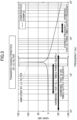
- FIG. 4 is a diagram that illustrates an example range for setting the resonance frequency of the LC filter.
- the carrier frequency for driving the inverter circuit 4 is f c
- the resonance frequency of the LC filter constituted by the reactor 8 and the capacitor 3a is f LC
- the maximum value of the output frequency of the inverter circuit 4 is MAX(f 0 ). If MAX(f 0 ) satisfies 6 ⁇ MAX f o ⁇ f LC ⁇ f c ⁇ 3 ⁇ MAX f o then, the characteristics of the LC filter can be set to a frequency band where harmonic components a, b, and c are not readily amplified.
- equation 1 when solved for MAX(f 0 ), is modified as follows: MAX f o ⁇ 1 6 f LC , and MAX f o ⁇ 1 3 f c ⁇ f LC
- the point where the power conversion apparatus is connected to the AC power supply 6 refers to, for example, AC input terminals of the power conversion apparatus 1A where a plurality of conductive lines 61, 62, and 63 are connected in the case of FIG. 1 , and AC input terminals of the power conversion apparatus 1B where a plurality of conductive lines 64 and 65 are connected in the case of FIG. 2 .
- the lower limit of C in equation 9 is infinitely close to zero when the power supply impedance on the AC power supply 6 side is infinite when viewed from the power conversion apparatus. Since the power supply impedance differs from country to country, the lower limit of C in equation 9 can be any value.
- the characteristics of the LC filter can be set to a frequency band where the harmonic components a, b, and c are not readily amplified.
- the resonance frequency of the LC filter is set in a region where above equation 1 or equation 2 does not hold. According to the technique of the present disclosure, the resonance frequency of the LC filter is set in a region where above equation 1 or equation 2 holds, so that it is possible to mitigate the amplification of harmonic components by the LC filter. As a result of this, abnormal generation of heat from the reactor 8, generation of excessive DC link voltage v dc , and so forth can be mitigated.
- the resonance frequency f LC is higher than 6 times MAX(f 0 ), for example, the amplification of harmonic components by the LC filter can be mitigated without introducing additional circuitry or special controls. Since the resonance frequency f LC is lower than f c - 3 times MAX(f 0 ), it is possible to mitigate the increase in circuit size due to, for example, addition of a noise filter necessitated by the increase of carrier frequency.
- MAX(f 0 ) is set to 600 Hz.
- 600 Hz is the upper limit of output frequency according to list control, so that list control can be satisfied.
- the gain of the LC filter at the carrier frequency f c is set to 0.1 or less.
- the gain of the LC filter at the carrier frequency fc becomes -20 dB (0.1 times) or less, so that the LC filter can reduce the harmonic components of the carrier frequency band.
- the gain of the LC filter at the carrier frequency f c is preferably 0.01 or less (-40 dB or less), and more preferably 0.001 or less (-60 dB or less).
- the gain of the LC filter at 6 times MAX(f 0 ) is set to 5 or less.
- the gain of the LC filter at 6 times MAX(f 0 ) becomes less than 14 dB (5 times).
- FIG. 5 shows a longitudinal cross-sectional view of an electrical unit with a power conversion apparatus.
- the electrical unit 10 illustrated in FIG. 5 includes a box-shaped housing 15 and a power conversion apparatus 20 housed in the housing 15.
- the power conversion apparatus 20 is an example of, for example, the above power conversion apparatus 1A.
- the power conversion apparatus 20 includes parts such as the converter circuit 2, the reactor 8, the capacitor 3a, the inverter circuit 4, the control part 5, and so forth. These parts inside the power conversion apparatus 20 are mounted on a substrate 60. By this means, the heat of these components such as the reactor 8 can be dissipated to the substrate 60.
- the substrate 60 is fixed to the inner surface of the housing 15.
- the substrate 60 is thermally coupled to a heat sink 47 via a thermally conductive coupling member 80, so that the heat of the substrate 60 can be dissipated from the heat sink 47.
- a through-hole 15d is formed in the housing 15 in the example illustrated in FIG. 5 .
- the substrate 60 is thermally coupled to the heat sink 47, which is provided outside the housing 15, via a coupling member 80 that penetrates the through-hole 15d.
- the technique of the present disclosure pertains to a case in which an LC filter's resonance frequency is set to satisfy equation 1 above, and the technique of patent document 1 pertains to a case in which an LC filter's resonance frequency is set to be greater than 40 times the power supply frequency.
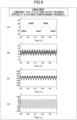
- FIG. 6 to FIG. 9 show cases in which the harmonic component b (which is a component six times the output frequency) appears.
- FIG. 6 and FIG. 7 show the waveforms of the power supply current i in of the AC power supply 6, the reactor current i L that flows in the reactor 8, the DC link voltage v dc in the DC link part 3, and the motor current i m that flows in the motor 7.
- FIG. 6 illustrates an embodiment to which the technique of the present disclosure is applied
- FIG. 7 shows a comparative example to which the technique of patent document 1 is applied.
- FIG. 9 show frequency analysis results of the waveforms of the power supply current i in of the AC power supply 6, the reactor current i L that flows in the reactor 8, the DC link voltage v dc in the DC link part 3, and the motor current i m that flows in the motor 7, based on the fast Fourier transform.
- FIG. 8 illustrates an embodiment to which the technique of the present disclosure is applied
- FIG. 9 shows a comparative example to which the technique of patent document 1 is applied.
- the harmonic component b (a component six times the output frequency) and the resonance frequency of the LC filter are close to each other. Consequently, the harmonic component b (a component six times the output frequency) causes the LC filter's resonance, and harmonic components near the resonance frequency appear in a noticeable manner.
- the harmonic component b (a component six times the output frequency) is set to be substantially smaller than the resonance frequency of the LC filter, so that amplification of the harmonic component b (a component six times the output frequency) is mitigated. In this way, as illustrated in FIG. 6 and FIG.
- the technique of the present disclosure reduces the harmonics superimposed on the power supply current i in , the reactor current i L , and the DC link voltage v dc , compared to the technique of patent document 1. Note that the conditions upon the simulations of FIG. 6 to FIG. 9 are shown in FIG. 14 .
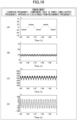
- FIG. 10 to FIG. 13 show cases in which the harmonic component c (carrier frequency - (a component that is three times the output frequency)) appears.
- FIG. 10 and FIG. 11 show the waveforms of the power supply current i in of the AC power supply 6, the reactor current i L that flows in the reactor 8, the DC link voltage v dc in the DC link part 3, and the motor current i m that flows in the motor 7.
- FIG. 10 shows an embodiment to which the technique of the present disclosure is applied
- FIG. 11 shows a comparative example to which the technique of patent document 1 is applied.
- FIG. 13 show frequency analysis results of the power supply current i in of the AC power supply 6, the reactor current i L that flows in the reactor 8, the DC link voltage v dc in the DC link part 3, and the motor current i m that flows in the motor 7, based on the fast Fourier transform.
- FIG. 12 shows an embodiment to which the technique of the present disclosure is applied, and FIG. 13 shows a comparative example to which the technique of patent document 1 is applied.
- the harmonic component c (carrier frequency - (a component that is three times the output frequency)) appears near the resonance frequency of the LC filter.
- the harmonic component c (carrier frequency - (a component three times the output frequency)) appears at a distance from the resonance frequency of the LC filter.
- the technique of the present disclosure reduces the peak of the harmonic component c (carrier frequency - (a component three times the output frequency)) on the lower frequency side, compared to the technique of patent document 1. In this way, as illustrated in FIG. 10 and FIG.
- harmonics superimposed on the power supply current i in , the reactor current i L , and the DC link voltage v dc are reduced, compared to the technique of patent document 1. Note that the conditions upon the simulations of FIG. 10 to FIG. 13 are shown in FIG. 15 .
- the LC filter is arranged in the DC link part 3.
- the reactor that constitutes the LC filter may be connected between the AC power supply 6 and the converter circuit 2.
- the capacitor 3a that constitutes the LC filter is arranged in the DC link part 3.
- the capacitor that constitutes the LC filter may be connected between the AC power supply 6 and the converter circuit 2, or the LC filter may be connected between the AC power supply 6 and the converter circuit 2.
- the LC filter may be placed anywhere insofar as a capacitor is connected between the reactor and the inverter circuit (inverter) that constitute the LC filter.
- the LC filter may be formed without a reactor.
- an LC filter may be formed with an inductance component of a conductive line and a capacitor.
Landscapes
- Engineering & Computer Science (AREA)
- Power Engineering (AREA)
- Chemical & Material Sciences (AREA)
- Combustion & Propulsion (AREA)
- Mechanical Engineering (AREA)
- General Engineering & Computer Science (AREA)
- Inverter Devices (AREA)
Applications Claiming Priority (2)
| Application Number | Priority Date | Filing Date | Title |
|---|---|---|---|
| JP2021061704 | 2021-03-31 | ||
| PCT/JP2022/016216 WO2022210950A1 (fr) | 2021-03-31 | 2022-03-30 | Dispositif de conversion de puissance, climatiseur et dispositif de réfrigération |
Publications (2)
| Publication Number | Publication Date |
|---|---|
| EP4318921A1 true EP4318921A1 (fr) | 2024-02-07 |
| EP4318921A4 EP4318921A4 (fr) | 2025-03-12 |
Family
ID=82610409
Family Applications (1)
| Application Number | Title | Priority Date | Filing Date |
|---|---|---|---|
| EP22781160.1A Pending EP4318921A4 (fr) | 2021-03-31 | 2022-03-30 | Dispositif de conversion de puissance, climatiseur et dispositif de réfrigération |
Country Status (5)
| Country | Link |
|---|---|
| US (1) | US12395097B2 (fr) |
| EP (1) | EP4318921A4 (fr) |
| JP (1) | JP7108224B1 (fr) |
| CN (1) | CN116868497A (fr) |
| WO (1) | WO2022210950A1 (fr) |
Family Cites Families (13)
| Publication number | Priority date | Publication date | Assignee | Title |
|---|---|---|---|---|
| JPS5329531A (en) * | 1976-08-31 | 1978-03-18 | Toshiba Corp | Filter circuit |
| JPS57126276A (en) * | 1981-01-27 | 1982-08-05 | Toshiba Corp | Starting method for power converter |
| JP4439846B2 (ja) * | 2003-06-24 | 2010-03-24 | 高橋 祐子 | 多相電流供給回路 |
| JP4595427B2 (ja) | 2004-02-06 | 2010-12-08 | パナソニック株式会社 | 電力変換装置 |
| US8902034B2 (en) * | 2004-06-17 | 2014-12-02 | Grant A. MacLennan | Phase change inductor cooling apparatus and method of use thereof |
| JP4067021B2 (ja) * | 2006-07-24 | 2008-03-26 | ダイキン工業株式会社 | インバータ装置 |
| JP5168955B2 (ja) * | 2007-03-14 | 2013-03-27 | パナソニック株式会社 | 電動機制御装置 |
| KR101564727B1 (ko) * | 2007-12-21 | 2015-10-30 | 엘지전자 주식회사 | 공기조화기 |
| JP5257533B2 (ja) * | 2011-09-26 | 2013-08-07 | ダイキン工業株式会社 | 電力変換装置 |
| JP5712987B2 (ja) * | 2012-09-27 | 2015-05-07 | ダイキン工業株式会社 | 電力変換装置の制御方法 |
| JP6685424B2 (ja) * | 2016-11-11 | 2020-04-22 | 三菱電機株式会社 | 電力変換装置及びこれを用いた空気調和装置 |
| US10680547B2 (en) * | 2018-07-12 | 2020-06-09 | Rockwell Automation Technologies, Inc. | Suppressing resonance in ultra long motor cable |
| JP2021061704A (ja) | 2019-10-08 | 2021-04-15 | 株式会社Nttファシリティーズ | 充放電計画作成装置及び充放電計画作成方法 |
-
2022
- 2022-03-28 JP JP2022051552A patent/JP7108224B1/ja active Active
- 2022-03-30 EP EP22781160.1A patent/EP4318921A4/fr active Pending
- 2022-03-30 US US18/547,940 patent/US12395097B2/en active Active
- 2022-03-30 CN CN202280014729.7A patent/CN116868497A/zh active Pending
- 2022-03-30 WO PCT/JP2022/016216 patent/WO2022210950A1/fr not_active Ceased
Also Published As
| Publication number | Publication date |
|---|---|
| JP2022159095A (ja) | 2022-10-17 |
| US20240235424A9 (en) | 2024-07-11 |
| US20240136949A1 (en) | 2024-04-25 |
| WO2022210950A1 (fr) | 2022-10-06 |
| EP4318921A4 (fr) | 2025-03-12 |
| CN116868497A (zh) | 2023-10-10 |
| JP7108224B1 (ja) | 2022-07-28 |
| US12395097B2 (en) | 2025-08-19 |
Similar Documents
| Publication | Publication Date | Title |
|---|---|---|
| Teichmann et al. | A comparison of three-level converters versus two-level converters for low-voltage drives, traction, and utility applications | |
| EP3267566B1 (fr) | Dispositif de conversion de puissance électrique | |
| CN104054245B (zh) | 功率转换装置 | |
| US5646498A (en) | Conducted emission radiation suppression in inverter drives | |
| US10736184B2 (en) | Power supply apparatus for induction heating | |
| WO2012070117A1 (fr) | Circuit d'attaque de moteur | |
| CN108631630B (zh) | 电力转换装置以及电力转换系统 | |
| JP6806280B1 (ja) | ノイズフィルタ及び電力変換装置 | |
| US10600716B2 (en) | Power converter | |
| CN1309155C (zh) | 开关电源电路和逆变装置 | |
| Lai et al. | Development of a 10 kW high power density three-phase ac-dc-ac converter using SiC devices | |
| JP6797748B2 (ja) | 電力変換装置及び電力変換システム | |
| JP7571417B2 (ja) | 電力変換装置 | |
| JP7133524B2 (ja) | 電力変換装置、鉄道車両電気システム | |
| EP4318921A1 (fr) | Dispositif de conversion de puissance, climatiseur et dispositif de réfrigération | |
| US11404970B2 (en) | Power converter | |
| Teichmann et al. | Three-level topologies for low voltage power converters in drives, traction and utility applications | |
| CN210535968U (zh) | 直流母排 | |
| US20250226768A1 (en) | Electric circuit | |
| US20250096695A1 (en) | Bus bar module and power conversion system | |
| CN218162235U (zh) | 无电解电容的变频电路及空调器 | |
| US20240396430A1 (en) | Common-mode voltage canceller | |
| CN112636578B (zh) | Pfc电路及降噪电路 | |
| WO2026013883A1 (fr) | Dispositif de conversion de puissance | |
| EP4657740A1 (fr) | Dispositif de conversion de puissance électrique |
Legal Events
| Date | Code | Title | Description |
|---|---|---|---|
| STAA | Information on the status of an ep patent application or granted ep patent |
Free format text: STATUS: THE INTERNATIONAL PUBLICATION HAS BEEN MADE |
|
| PUAI | Public reference made under article 153(3) epc to a published international application that has entered the european phase |
Free format text: ORIGINAL CODE: 0009012 |
|
| STAA | Information on the status of an ep patent application or granted ep patent |
Free format text: STATUS: REQUEST FOR EXAMINATION WAS MADE |
|
| 17P | Request for examination filed |
Effective date: 20230922 |
|
| AK | Designated contracting states |
Kind code of ref document: A1 Designated state(s): AL AT BE BG CH CY CZ DE DK EE ES FI FR GB GR HR HU IE IS IT LI LT LU LV MC MK MT NL NO PL PT RO RS SE SI SK SM TR |
|
| DAV | Request for validation of the european patent (deleted) | ||
| DAX | Request for extension of the european patent (deleted) | ||
| P01 | Opt-out of the competence of the unified patent court (upc) registered |
Free format text: CASE NUMBER: APP_38436/2024 Effective date: 20240627 |
|
| REG | Reference to a national code |
Ref country code: DE Ref legal event code: R079 Free format text: PREVIOUS MAIN CLASS: H02M0007480000 Ipc: H02M0007538700 |
|
| A4 | Supplementary search report drawn up and despatched |
Effective date: 20250212 |
|
| RIC1 | Information provided on ipc code assigned before grant |
Ipc: F24F 11/88 20180101ALI20250206BHEP Ipc: H02P 27/08 20060101ALI20250206BHEP Ipc: H02M 1/14 20060101ALI20250206BHEP Ipc: H02M 1/12 20060101ALI20250206BHEP Ipc: H02M 5/458 20060101ALI20250206BHEP Ipc: H02M 7/5387 20070101AFI20250206BHEP |