EP4325269A1 - Dispositif de balayage optique - Google Patents
Dispositif de balayage optique Download PDFInfo
- Publication number
- EP4325269A1 EP4325269A1 EP22804485.5A EP22804485A EP4325269A1 EP 4325269 A1 EP4325269 A1 EP 4325269A1 EP 22804485 A EP22804485 A EP 22804485A EP 4325269 A1 EP4325269 A1 EP 4325269A1
- Authority
- EP
- European Patent Office
- Prior art keywords
- mirror
- shielding plate
- optical path
- optical
- light beam
- Prior art date
- Legal status (The legal status is an assumption and is not a legal conclusion. Google has not performed a legal analysis and makes no representation as to the accuracy of the status listed.)
- Granted
Links
Images





Classifications
-
- G—PHYSICS
- G02—OPTICS
- G02B—OPTICAL ELEMENTS, SYSTEMS OR APPARATUS
- G02B27/00—Optical systems or apparatus not provided for by any of the groups G02B1/00 - G02B26/00, G02B30/00
- G02B27/01—Head-up displays
- G02B27/017—Head mounted
- G02B27/0172—Head mounted characterised by optical features
-
- G—PHYSICS
- G02—OPTICS
- G02B—OPTICAL ELEMENTS, SYSTEMS OR APPARATUS
- G02B26/00—Optical devices or arrangements for the control of light using movable or deformable optical elements
- G02B26/08—Optical devices or arrangements for the control of light using movable or deformable optical elements for controlling the direction of light
- G02B26/0816—Optical devices or arrangements for the control of light using movable or deformable optical elements for controlling the direction of light by means of one or more reflecting elements
- G02B26/0833—Optical devices or arrangements for the control of light using movable or deformable optical elements for controlling the direction of light by means of one or more reflecting elements the reflecting element being a micromechanical device, e.g. a MEMS mirror, DMD
-
- G—PHYSICS
- G02—OPTICS
- G02B—OPTICAL ELEMENTS, SYSTEMS OR APPARATUS
- G02B5/00—Optical elements other than lenses
- G02B5/005—Diaphragms
-
- G—PHYSICS
- G02—OPTICS
- G02B—OPTICAL ELEMENTS, SYSTEMS OR APPARATUS
- G02B27/00—Optical systems or apparatus not provided for by any of the groups G02B1/00 - G02B26/00, G02B30/00
- G02B27/01—Head-up displays
- G02B27/0101—Head-up displays characterised by optical features
- G02B2027/0118—Head-up displays characterised by optical features comprising devices for improving the contrast of the display / brillance control visibility
-
- G—PHYSICS
- G02—OPTICS
- G02B—OPTICAL ELEMENTS, SYSTEMS OR APPARATUS
- G02B27/00—Optical systems or apparatus not provided for by any of the groups G02B1/00 - G02B26/00, G02B30/00
- G02B27/01—Head-up displays
- G02B27/017—Head mounted
- G02B2027/0178—Eyeglass type
Definitions
- the present invention relates to an optical scanning device having a MEMS optical deflector.
- Patent Literature 1 discloses an optical scanning device having a MEMS optical deflector.
- the optical scanning device is attached to a temple (side support) on one side of a spectacles-type head mount, emits scanning light from the MEMS optical deflector toward lenses and half mirrors arranged toward the front (front frame) of the spectacles, and projects an image on the user's retina by the scanning light reflected by the half mirror.
- the lens and the half mirror are mounted on the temple in addition to the optical scanning device, and the optical scanning device faces the half mirror with the lens interposed therebetween.
- Laser light emitted from the optical scanning device scans on the half mirror along the mirror surface thereof, is reflected by the mirror surface, and projects an image onto the retina of a user's eye.
- Patent Literature 1 Japanese Patent No. 6734532
- Patent Literature 1 does not disclose in what positional relationship, the light source, the MEMS optical deflector, and the substrate are mounted in the optical scanning device specifically.
- An object of the present invention is to provide an optical scanning device which has improved the quality of a light beam emitted as scanning light.
- An optical scanning device of the present invention includes:
- a shielding plate arranged for a corresponding optical path generation mirror has an aperture.
- a light beam can be improved into a light beam with high contrast as a result of cutting a peripheral low brightness area by the aperture.
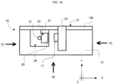
- FIG. 1A is a plan view of an optical scanning device 10
- FIG. 1B is a view taken along arrow 1B in FIG. 1A
- FIG. 1C is a view taken along arrow 1C in FIG. 1A
- FIG. 1D is a view taken along arrow 1D in FIG. 1A .
- FIGS. 1A to 1D show the optical scanning device 10 with a cover 33 (one-dot chain line in FIG. 1B ) removed.
- the optical scanning device 10 includes a support frame body 12.
- the support frame body 12 has an L-shaped cross-sectional contour, and has a bottom plate portion 13a and an uprising plate portion 13b which are vertically connected.
- a substrate 15 is rectangular and placed onto and fixed to an upper surface of the bottom plate portion 13a.
- An X-axis and a Y-axis are defined as axes in the directions parallel to the longitudinal direction (direction parallel to the long side) and the lateral direction (direction parallel to the short side) of the substrate 15, respectively.
- a Z-axis is defined as an axis parallel to the uprising direction of the uprising plate portion 13b from the substrate 15.
- Lp indicates a light beam.
- the course of the light beam Lp means an optical path of the light beam Lp.
- Cl is an optical axis as a central axis of the optical path of the light beam Lp.
- the optical path is static between a VCSEL 17 and a MEM optical deflector 20. Since the light beam Lp is emitted from the MEM optical deflector 20 as scanning light, an optical path on the downstream side from the MEMS optical deflector 20 becomes dynamic.
- the light beam Lp is emitted from the left side of FIG. 1B , i.e., from the negative end of the optical scanning device 10 in the X-axis direction. Therefore, in the X-axis, the negative side and the positive side will be appropriately referred to as the front and rear of the optical scanning device 10, respectively. Further, since the positive side and the negative side in the Z-axis direction are respectively taken as an upper surface and a lower surface in the substrate 15, the positive side and the negative side in the Z-axis direction will be appropriately defined as above and below the optical scanning device 10.
- the VCSEL 17 and the MEMS optical deflector 20 are mounted on the upper surface of the substrate 15 with the X-axis direction as an arrangement direction.
- the VCSEL 17 has an emission unit 18 on its upper surface and emits laser light upward, i.e., just above in parallel to the Z-axis direction from the emission unit 18.
- the MEMS optical deflector 20 directs a mirror surface of a rotating mirror 21 upward.
- the MEMS optical deflector 20 is a two-dimensional scanning MEMS optical deflector in the present embodiment, it may be a one-dimensional scanning MEMS optical deflector.
- the configuration of the MEMS optical deflector itself is known in various ways.
- the MEMS optical deflectors described in Japanese Patent Application Laid-Open No. 2017-207630 (two-dimensional scanning MEMS optical deflector) and Japanese Patent Application Laid-Open No. 2014-056020 (one-dimensional scanning MEMS optical deflector) are selected.
- a lens 19 ( FIG. 1B ) is arranged directly above the emission unit 18 in proximity to the emission unit 18.
- the VCSEL 17 is illustrated as a single body, but in an actual product, it is enclosed in a package (not shown).
- the package which encloses the VCSEL 17 therein is made of a transparent material such as quartz glass at a portion through which the light beam from the emission unit 18 is emitted (for example: Japanese Patent No. 4512330 and Japanese Patent Application Laid-Open No. 2009-027088 ).
- the lens 19 is fixed (for example, glued) to an inner or outer surface of such a transparent material, or a transparent part itself thereof is processed as a lens, so that the position directly above the emission unit 18 is held.
- FIG. 2 is a side view of the support frame body 12. Description will be made about the support frame body 12, a plate-like mirror 23, and a rotary type mirror 25 with reference to FIGS. 1A to 1D and FIG. 2 .
- the uprising plate portion 13b of the support frame body 12 has an inclined groove 30 and a through hole 31.
- the inclined groove 30 has a rectangular cross section and opens obliquely rearward upward along the side contour of the uprising plate portion 13b.
- a bottom surface of the inclined groove 30 is formed of an inclination surface inclined at 45° with respect to the substrate 15.
- the through hole 31 is formed as a cylindrical hole penetrating through the uprising plate portion 13b in the Y-axis direction.
- the center of the width (length in side view in FIG. 1B ) of the inclination surface (bottom surface) of the inclined groove 30 is located at the same position as the emission unit 18 of the VCSEL 17.
- a center line Co of the cylindrical hole of the through hole 31 is positioned between the VCSEL 17 and the rotating mirror 21 of the MEMS optical deflector 20 in the X-axis direction.
- the center of the length of the inclination surface of the inclined groove 30 and the center line of the cylindrical hole of the through hole 31 are located at the same position in the Z-axis direction, that is, at the same height from the substrate 15.
- the plate-like mirror 23 is made of a rectangular plate-like member and has one end adhered to a slope portion of the inclined groove 30 in a cantilevered state with an adhesive member such as a resin with the lower plate surface thereof used as a mirror surface.
- the plate thickness of the plate-like mirror 23 is set substantially equal to the depth of the inclined groove 30.
- the plate width (length in side view in FIG. 1B ) of the plate-like mirror 23 is slightly shorter than the width (length in side view in FIG. 1B ) of the inclined groove 30. Therefore, before one end of the plate-like mirror 23 is adhered to the inclined groove 30, that is, in a state before the one end is fixed, the plate-like mirror 23 is slightly displaceable in the direction of the slope of the bottom surface within the inclined groove 30 and is capable of changing the angle of rotation around the axial line parallel to the Y-axis. Such a change enables adjustment of the orientation of the mirror surface of the plate-like mirror 23 when manufacturing the optical scanning device 10. By adhesion of one end of the plate-like mirror 23 to the inclined groove 30, the plate-like mirror is fixed so that it cannot be displaced.
- the rotary type mirror 25 has a flat plate-like mirror portion 26 and a cylindrical fitting end portion 27 which is coupled to one end of the mirror portion 26 and fits into the through hole 31.
- the diameter of the fitting end portion 27 is slightly smaller than the diameter of the through hole 31. Therefore, before adhesion of the fitting end portion 27 to the through hole 31, i.e., in a state before fixing thereof, the rotary type mirror 25 is rotatable about the center line of the through hole 31 while fitting the fitting end portion 27 into the through hole 31, and can be tilted within a predetermined inclination angle range from a state in which the center line of the rotary type mirror 25 is aligned with the center line Co ( FIG. 1B ) of the through hole 31.
- the rotary type mirror 25 is rotatably displaceable in a larger angle range than the plate-like mirror 23.
- Such a rotatable and tiltable configuration enables adjustment of the orientation of the mirror surface as the lower surface of the mirror portion 26 when manufacturing the optical scanning device 10, and then allows the fitting end portion 27 to be fixed so as not to rotate by adhering it with an adhesive member such as a resin.
- the rotating mirror 21 of the MEMS optical deflector 20 is not positioned directly below the rotary type mirror 25 with respect to the rotary type mirror 25 but is positioned on the front side, i.e., on the negative side with respect to the rotary type mirror 25 in the X-axis direction. In other words, the rotating mirror 21 of the MEMS optical deflector 20 is positioned obliquely downward when viewed from the rotary type mirror 25.
- this configuration contributes to causing the light beam Lp from the optical scanning device 10 to be emitted obliquely forward rather than perpendicular to the substrate 15 in regard to its emission direction.
- This configuration ensures that when the optical scanning device 10 is attached to the temple of a spectacle body as a spectacles-type video display device 155 (video scanning device of smart glass) described as a use example of the optical scanning device in the next FIG. 3 , the light emitted from the optical scanning device 10 reaches the lens inner surface of the spectacle body without being interfered by the user's face from a slight gap between an imaging device and the user's face.
- FIG. 3 is a view showing the spectacles-type video display device 155 as an application example of the optical scanning device 10.
- the spectacles-type video display device 155 will be briefly described.
- the spectacles-type video display device 155 includes a spectacle body 160 and a video generation device 110 detachably attached to the spectacle body 160 by a mounting member such as a clip 170.
- the spectacle body 160 includes left and right temples 161a and 161b and a front frame 163 coupled to front ends of the left and right temples 161a and 161b at both left and right ends.
- the front frame 163 further includes left and right lens frame portions 164a and 164b, and a bridge 165 connecting the left and right lens frame portions 164a and 164b.
- the optical scanning device 10 is incorporated in one-row arrangement within the video generation device 110 together with other elements (for example: buffer amplifier for MEMS sensor and LDD (laser driver)) along the extension direction of the temple 161b of the spectacle body 160.
- the optical scanning device 10 is arranged in the forefront, that is, closest to the lens 167 side.
- the light beam Lp ( FIG. 1B or FIG. 4A ) emitted from the optical scanning device 10 scans a scanning region 172 as a region on the inner surface side of the lens 167.
- the scanning region 172 is a half mirror, and the light beam Lp is reflected by the scanning region 172 to generate an image on the user's retina with the retina as a screen.
- the cover 33 ( FIG. 1B ) extends along the contour of the uprising plate portion 13b above the substrate 15, and is placed over the uprising plate portion 13b to fix an opening peripheral edge on the lower end side thereof to the peripheral edge of the bottom plate portion 13a.
- the cover 33 has a transparent portion 34 at least at a portion where a light beam Lp to be described later is emitted from the optical scanning device 10 as scanning light.
- FIG. 4A is a detailed view of a positional relationship of optical elements of the optical scanning device 10 in which the optical path of the light beam Lp is arranged
- FIG. 4B is a view taken along arrow 4B in FIG. 4A
- FIG. 4C is a view taken along arrow 4C in FIG. 4A
- FIG. 4D is a view taken along arrow 4D in FIG. 4A
- FIG. 4E is a view taken along arrow 4E in FIG. 4A
- FIG. 4C is also a view taken along arrow 4C' in FIG. 4A .
- the arrows 4B to 4E and 4C' in FIG. 4A are all located on the optical axis Cl.
- FIG. 4A the right side on the drawing is forward in the negative direction of the X-axis, and the left side thereon is backward in the positive direction of the X-axis.
- the lens 19 and the plate-like mirror 23 are arranged directly above the emission unit 18.
- the plate-like mirror 23 has a mirror surface which faces obliquely downward toward the rotary type mirror 25.
- a shielding plate 41 has an elliptical aperture 42 and is fixed (e.g., glued) to the mirror surface of the plate-like mirror 23. Consequently, the mirror surface of the plate-like mirror 23 allows the light beam Lp to enter and exist only within the range of the elliptical aperture 42.
- the lens 19 is positioned between the emission unit 18 and the plate-like mirror 23 in the optical path of the light beam Lp and emits the light beam Lp emitted from the emission unit 18 while expanding in the radial direction so as to converge on a predetermined point (in this example, a light spot 51 on a projection screen 50) downstream of the MEMS optical deflector 20.
- a predetermined point in this example, a light spot 51 on a projection screen 50
- the mirror surface of the mirror portion 26 faces obliquely downward toward the plate-like mirror 23 side.
- the optical axis Cl extends parallel to the substrate 15 between the plate-like mirror 23 and the mirror portion 26.
- a shielding plate 45 has an elliptical aperture 46 and is fixed (e.g., glued) to the mirror surface of the mirror portion 26.
- the plate-like mirror 23 has a lower surface as the mirror surface.
- the shielding plate 41 has the elliptical aperture 42 and is fixed to the mirror surface of the plate-like mirror 23.
- the mirror surface of the plate-like mirror 23 allows the light beam Lp to enter and exit only within the range of the elliptical aperture 42.
- the light spot 51 is generated on the projection screen 50 as a condensing point of the light beam Lp by the lens 19.
- the projection screen 50 will be a location a predetermined distance away from the optical scanning device 10 along the optical path of the light beam Lp.
- the projection screen 50 becomes the user's retina.
- the light beam Lp emitted from the emission unit 18 of the VCSEL 17 is laser light weakened enough to not harm human eyes.
- the light beam Lp is emitted from the emission unit 18 of the VCSEL 17 while spreading radially upward (positive direction in the Z-axis direction) perpendicular to the substrate 15. After passing through the lens 19, the light beam Lp advances along the optical path while reducing in the radial direction until it reaches the condensing point (light spot 51 in the optical scanning device 10) of the lens 19. After passing through the lens 19, the light beam Lp passes through the elliptical aperture 42 of the shielding plate 41 and reaches the plate-like mirror 23.
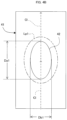
- the elliptical aperture 42 is an ellipse as shown in FIG. 4B when viewed from the direction perpendicular to the shielding plate 41 (the normal direction of the plate-like mirror 23).
- the shielding plate 41 has a surface inclined with respect to the optical axis Cl.
- the major axis of the elliptical aperture 42 overlaps the optical axis Cl of the light beam Lp when viewed from the direction (normal direction) perpendicular to the shielding plate 41.
- Da1 and Db1 are the dimensions of the major axis and minor axis of the ellipse. Further, Da1/Db1 is defined as ⁇ 1.
- the elliptical aperture 42 is closer to a perfect circle than when viewed from the direction (normal direction) perpendicular to the shielding plate 41. That is, when the elliptical aperture 42 is viewed from the direction of the optical axis Cl, it is a circular shape in which the ratio of the major axis to the minor axis of the ellipse in FIG. 4C (in FIG. 4C , the elliptical aperture 42 is an ellipse including a perfect circle) is closer to 1 than ⁇ 1 (1 ⁇ 1).
- FIG. 4C the elliptical aperture 42 is an ellipse including a perfect circle
- the vertical axis becomes the major axis and the horizontal axis becomes the minor axis.
- the diameter of the circle (the average value of the major and minor axes in the case of the ellipse) when viewed along the optical axis Cl is defined as ⁇ 1.
- the light beam Lp which is emitted from the emission unit 18 of the VCSEL 17, passes through the lens 19 and is condensed becomes a shape close to a perfect circle at any position on the optical axis Cl when viewed in the direction of the optical axis Cl ( FIG. 4C ).
- the light beam Lp generates an elliptical irradiation shape Lp1 at the shielding plate 41 arranged obliquely with respect to the optical axis Cl ( FIG. 4B ).
- the elliptical aperture 42 becomes an ellipse which is substantially similar in shape to the irradiation shape Lp1 but slightly smaller than it.
- the elliptical aperture 42 is included inside the irradiation shape Lp1. By doing so, the light beam Lp holds the shape close to the original perfect circle when viewed from the direction of the optical axis Cl even after being reflected by the plate-like mirror 23 and passing through the elliptical aperture 42.
- the act of making the elliptical aperture 42 into the shape substantially similar to the irradiation shape Lp1 is limited to the case where the shielding plate 41 is thin in thickness.
- the shape is slightly deformed from the similar shape.
- the plate-like mirror 23 is adjusted in inclination angle as described above, the inclination angle of the fixed shielding plate 41 changes, and the accurate shape of the irradiation shape Lp1 is determined after the adjustment.
- the relationship between the shapes of the elliptical aperture 42 and the irradiation shape Lp1 may deviate from similarity, but the direction of the maj or axis always becomes the direction of inclination of the shielding plate 41 with respect to the optical axis Cl.
- the ellipse of the elliptical aperture 42 and the ellipse of the irradiation shape Lp1 have the intersection of the major and minor axes as the central position at the same location ( FIG. 4B ).
- a predetermined value ⁇ 1 is defined for the illuminance ⁇ in the cross section.
- the illuminance ⁇ in the cross section of the light beam Lp is maximum in the center of the cross section, i.e., at the point of intersection with the optical axis Cl, and decreases as it moves away from the optical axis Cl in the radial direction, finally resulting in 0.
- the irradiation shape Lp1 is defined as a region in which the illuminance ⁇ is equal to or greater than a predetermined value ⁇ 2 (0 ⁇ 2 ⁇ 1).
- the predetermined values ⁇ 1 and ⁇ 2 are 0.5 and 0.3 times the maximum value of the illuminance ⁇ , respectively.
- the illuminance of the light spot 51 on the projection screen 50 is assumed to be the illuminance generated by converging the incident points of the respective light rays on the projection screen 50 to the light spot 51.
- the light beam Lp is cut in the peripheral edge in the cross section, in other words, in a radially outer region in which the illuminance ⁇ is less than ⁇ 1.
- the region inside the irradiation shape Lp1 and outside the elliptical aperture 42 in FIG. 4B is the region to be cut.
- the light beam Lp immediately after being reflected by the plate-like mirror 23 and emitted from the elliptical aperture 42 becomes a light beam which is ⁇ 1 or more in the illuminance ⁇ and circular in cross section.
- the light beam Lp then travels along the optical path toward the rotary type mirror 25.
- the light beam Lp passes through the elliptical aperture 46 of the shielding plate 45 and reaches the rotary type mirror 25.
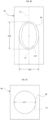
- the elliptical aperture 46 is an ellipse when viewed in the direction of the optical axis Cl from the direction (the normal direction of the rotary type mirror 25) perpendicular to the shielding plate 45 ( FIG. 4D ).
- An irradiation shape Lp2 of the irradiation region of the light beam Lp within the elliptical aperture 46 is an ellipse and is generated inside the ellipse of the elliptical aperture 46.
- the elliptical aperture 46 is closer to a perfect circle than when viewed from the vertical direction, i.e., a circular shape in which the ratio between the major and minor axes is closer to 1 than ⁇ 2.
- the diameter ⁇ of this circle is assumed to be ⁇ 2. ⁇ 1> ⁇ 2 ismade.
- the light beam Lp passes through the elliptical aperture 46 and is then irradiated to the rotary type mirror 25 in an irradiation shape Lp2.
- the irradiation shape Lp2 is an elliptical shape smaller than the elliptical aperture 46.
- the light beam Lp generates diffracted light when passing through the elliptical aperture 42 of the shielding plate 41.
- the diffracted light is weal light which spreads over a range larger than the light beam Lp.
- the shielding plate 45 prevents the diffracted light from being reflected by the rotary type mirror 25.
- the irradiation shape Lp2 is smaller than the elliptical aperture 46, and the entirety of the irradiation shape Lp2 is accommodated inside the elliptical aperture 46, thereby preventing the diffracted light from being further generated from the shielding plate 45.
- the light beam Lp emitted from the elliptical aperture 46 travels obliquely downward (direction away from the plate-like mirror 23 in the X-axis direction) and reaches the center of the rotating mirror 21 of the MEMS optical deflector 20.
- the rotating mirror 21 of the MEMS optical deflector 20 rotates around two mutually intersecting axes with non-resonance and resonance, respectively.
- the two axes are parallel to the X-axis and the Y-axis respectively when the rotating mirror 21 is stationary.
- the light beam Lp emitted from the rotating mirror 21 becomes scanning light for two-dimensional scanning due to the reciprocating rotation of the rotating mirror 21 about the two axes.
- the resonant frequency and the non-resonant frequency are, for example, 14 kHz or higher and 60 Hz, respectively.
- the (non- resonance side) reciprocating rotation angle of the rotating mirror 21 about the X-axis is smaller than the (resonance side) reciprocating rotation angle of the rotating mirror 21 about the Y-axis.
- the reciprocating rotation of the rotating mirror 21 about the resonant axis and the reciprocating rotation of the rotating mirror 21 about the non-resonant axis will be explained as respectively corresponding to the horizontal and vertical directions of the projection screen 50 to be described later.
- the light beam Lp becomes scanning light by being reflected by the rotating mirror 21 and is emitted from the optical scanning device 10 to scan on the projection screen 50 outside the optical scanning device 10.
- a light spot 51 is generated at an irradiation point of the light beam Lp on the projection screen 50.
- the light spot 51 scanning over the projection screen 50 generates a rectangular image region with the horizontal and vertical directions taken as the major and minor sides respectively.
- the elliptical aperture 42 on the upstream side is larger in area than the elliptical aperture 46 on the downstream side.
- Both the elliptical apertures 42 and 46 are circular when viewed from the upstream side in the direction of the optical axis Cl, but the elliptical aperture 42 on the upstream side is larger in its circle diameter than the elliptical aperture 46 on the downstream side.
- the shaping effect of the cross section of the light beam Lp can be enhanced. Further, the contrast between the light spot 51 and its surroundings can be improved more than one-step periphery cut.
- the shielding plates 41 and 45 are attached to the plate-like mirror 23 and the rotary type mirror 25 by means of bonding such as adhesion or the like.
- the projection screen 50 is a plane perpendicular to the optical axis Cl in a state in which the MEMS optical deflector 20 is stopped.
- the light spot 51 is designed so that the ratio of the major axis to the minor axis approaches 1 with the perfect circle being ideal.
- the projection screen 50 may be a surface inclined with respect to the optical axis Cl in the state in which the MEMS optical deflector 20 is stopped, depending on the application and the arrangement of members.
- the retina corresponds to the projection screen 50, but the optical scanning device 10 may be placed at a position where the optical axis Cl of the light beam Lp in the stopped state of the MEMS optical deflector 20 is tilted with respect to the assumed position of the retina.
- the formed light spot 51 is deformed into a shape extending in the direction of inclination of the optical axis Cl of the light beam Lp.
- Such deformation of the light spot 51 due to the position of the projection screen 50 may also occur in other applications, a projector, etc.
- a wall perpendicular to the plane on which the projector is placed can be assumed as the projection screen 50.
- the sectional shape perpendicular to the optical axis Cl at the light beam Lp emitted from the optical scanning device 10 into an elliptical shape having a major axis in the inclination and vertical directions of the optical axis Cl to the projection screen 50 assumed in advance in the stopped state of the MEMS optical deflector 20.
- FIG. 6 is a view showing the shape of the light spot 51 when the projection screen 50 is inclined with respect to the optical axis Cl.
- the inclination angle of the projection screen 50 is defined as 0° when the screen surface of the projection screen 50 becomes a plane perpendicular to the optical axis Cl of the light beam Lp.
- the light beam Lp whose cross section perpendicular to the optical axis Cl is elliptical, becomes a perfect circle on the projection screen 50. Even if the light beam Lp is not exactly formed into the perfect circle, the ratio of the major axis to the minor axis of the light spot 51 on the projection screen 50 can be brought close to 1 by using such a light beam Lp.
- the sectional shape of the light beam Lp perpendicular to the optical axis Cl is called a cross-sectional shape.
- the cross-sectional shape of the light beam Lp can be shaped by adjusting the shapes of the elliptical aperture 42 of the shielding plate 41 and the elliptical aperture 46 of the shielding plate 45.
- the contrast of the light spot 51 on the projection screen 50 is enhanced by cutting the periphery of the light beam Lp with the elliptical apertures 42 and 46. As a result, the quality of video viewed by the user can be enhanced.
- the diameter of the cross section of the light beam Lp is made narrow by condensing by the lens 19 ( FIG. 4A ), but the light beam Lp may be parallel light whose diameter of cross section is constant. Incidentally, even when the light is made to be parallel light, it is referred to as the lens 19.
- the number of VCSELs 17 is not limited to one.
- VCSELs 17 of three colors of RGB may be used side by side.
- the plate-like mirror 23 is arranged for each VCSEL 17.
- the plate-like mirror 23 is a dichroic mirror, each VCSEL 17 can be aligned.
- the two shielding plates 41 and 45 are used, at least one shielding plate is sufficient in the present invention.
- FIG. 7 is a schematic view of a main part of an optical scanning device 61 equipped with VCSELs 17R, G, and B of RGB.
- the VCSELs 17R, G, and B are mounted in a row in an X-axis direction on the common substrate 15 ( FIG. 1A ).
- a lens 19 and a dichroic mirror 65 are arranged directly above each of the VCSELs 17R, G, and B so as to face each other.
- the light beam Lp is directed toward a rotary type mirror 25 in parallel to the substrate 15, cut at the peripheral edge thereof by an elliptical aperture 46 of the shielding plate 45, and then directed toward a MEMS optical deflector 20.
- the optical scanning device 61 does not have the shielding plate 41.
- the elliptical aperture 46 of the shielding plate 45 is smaller than the irradiation region of the light beam Lp for the shielding plate 45, and has the function of shaping the light beam Lp, i.e., the same function as that of the elliptical aperture 42 in the embodiment of FIG. 4 .
- FIG. 5 is a configuration view of a main part of an optical scanning device 10 having a concave mirror 53 instead of the plate-like mirror 23.
- the concave mirror 53 is fixed (e.g., glued) to a shielding plate 41 at its peripheral edge so as to face an elliptical aperture 42 from the upper surface side of the shielding plate 41.
- the concave mirror 53 can also be manufactured by integral molding with the shielding plate 41 using a predetermined mold form, for example.
- one end of the shielding plate 41 is extended toward an inclined groove 30 ( FIG. 2 , etc.) and directly fixed to the inclined groove 30.
- the VCSEL 17 is used as the light source.
- the light source of the present invention is not limited to the VCSEL 17, and other than the VCSEL 17, for example, an edge emitting laser can also be selected.
- the VCSEL 17 emits light directly above the light beam Lp.
- the light source does not have to emit a light beam upward (e.g., directly above).
- a plurality of optical path generation mirrors generate an optical path so as to make the light beam emitted from the light source enter the mirror portion of the MEMS optical deflector.
- the shielding plates 41 and 45 are both attached to a plate-like mirror 23 and a rotary type mirror 25 as their corresponding optical path generation mirrors by mounting or the like.
- the shielding plate can also be arranged on the optical path upstream of the corresponding optical path generation mirror separately from the corresponding optical path generation mirror. In that case, the shielding plate arranged on the upstream side of the corresponding optical path generation mirror separately from the corresponding optical path generation mirror must be arranged so as not to interfere with the optical path on the downstream side of the corresponding optical path generation mirror.
- the shielding plates 41 and 45 are arranged parallel to the plate-like mirror 23 and the rotary type mirror 25 as the corresponding optical path generation mirrors.
- the mirror surface is a curved surface in the concave mirror 53 in FIG. 5 .
- the normal line is set at the intersection where the incident side optical axis Cl, the shielding plate, and the optical path generation mirror intersect, and the normal line of the shielding plate with respect to the incident side optical axis Cl and the normal line of the optical path generation mirror are defined as the inclination angles of the shielding plate and the optical path generation mirror.
- the inclination angles of the shielding plate and the optical path generation mirror at that time become 0° when the inclination angle of the plane perpendicular to the light beam Lp at the intersection is defined as 0°.
Landscapes
- Physics & Mathematics (AREA)
- General Physics & Mathematics (AREA)
- Optics & Photonics (AREA)
- Mechanical Optical Scanning Systems (AREA)
Applications Claiming Priority (2)
| Application Number | Priority Date | Filing Date | Title |
|---|---|---|---|
| JP2021085237A JP7643933B2 (ja) | 2021-05-20 | 2021-05-20 | 光走査装置 |
| PCT/JP2022/018037 WO2022244571A1 (fr) | 2021-05-20 | 2022-04-18 | Dispositif de balayage optique |
Publications (3)
| Publication Number | Publication Date |
|---|---|
| EP4325269A1 true EP4325269A1 (fr) | 2024-02-21 |
| EP4325269A4 EP4325269A4 (fr) | 2024-12-25 |
| EP4325269B1 EP4325269B1 (fr) | 2026-05-06 |
Family
ID=84141340
Family Applications (1)
| Application Number | Title | Priority Date | Filing Date |
|---|---|---|---|
| EP22804485.5A Active EP4325269B1 (fr) | 2021-05-20 | 2022-04-18 | Dispositif de balayage optique |
Country Status (5)
| Country | Link |
|---|---|
| US (1) | US20240241367A1 (fr) |
| EP (1) | EP4325269B1 (fr) |
| JP (1) | JP7643933B2 (fr) |
| CN (1) | CN117321470A (fr) |
| WO (1) | WO2022244571A1 (fr) |
Families Citing this family (2)
| Publication number | Priority date | Publication date | Assignee | Title |
|---|---|---|---|---|
| JP7643887B2 (ja) * | 2021-02-22 | 2025-03-11 | スタンレー電気株式会社 | 眼鏡型映像表示装置 |
| JP2023172527A (ja) * | 2022-05-24 | 2023-12-06 | 富士通株式会社 | レーザセンサ |
Family Cites Families (12)
| Publication number | Priority date | Publication date | Assignee | Title |
|---|---|---|---|---|
| US5347121A (en) * | 1992-12-18 | 1994-09-13 | Spectra-Physics Scanning Systems, Inc. | Variable focus optical system for data reading |
| JP4512330B2 (ja) | 2002-07-12 | 2010-07-28 | 株式会社リコー | 複合光学素子、及び光トランシーバー |
| JP4965935B2 (ja) * | 2006-08-24 | 2012-07-04 | キヤノン株式会社 | 光偏向器、光走査装置及び走査型画像表示装置 |
| JP5115073B2 (ja) | 2007-07-23 | 2013-01-09 | 富士ゼロックス株式会社 | 半導体発光装置 |
| JP5079060B2 (ja) * | 2010-08-02 | 2012-11-21 | シャープ株式会社 | 光走査装置および画像形成装置 |
| JP5705151B2 (ja) * | 2012-02-24 | 2015-04-22 | 京セラドキュメントソリューションズ株式会社 | 光走査装置、画像形成装置 |
| JP6049364B2 (ja) | 2012-09-11 | 2016-12-21 | スタンレー電気株式会社 | 光偏向器 |
| JP2015022158A (ja) * | 2013-07-19 | 2015-02-02 | 株式会社リコー | 光走査装置および画像表示装置 |
| JP6734532B2 (ja) | 2016-04-22 | 2020-08-05 | ミツミ電機株式会社 | 表示装置 |
| JP2017207630A (ja) | 2016-05-18 | 2017-11-24 | スタンレー電気株式会社 | 光偏向器 |
| JP6227177B1 (ja) * | 2017-01-20 | 2017-11-08 | 株式会社Qdレーザ | 画像投影装置 |
| JP7052577B2 (ja) * | 2018-06-07 | 2022-04-12 | 株式会社リコー | 光学装置、映像表示装置、及び検眼装置 |
-
2021
- 2021-05-20 JP JP2021085237A patent/JP7643933B2/ja active Active
-
2022
- 2022-04-18 EP EP22804485.5A patent/EP4325269B1/fr active Active
- 2022-04-18 CN CN202280035577.9A patent/CN117321470A/zh active Pending
- 2022-04-18 US US18/562,009 patent/US20240241367A1/en active Pending
- 2022-04-18 WO PCT/JP2022/018037 patent/WO2022244571A1/fr not_active Ceased
Also Published As
| Publication number | Publication date |
|---|---|
| EP4325269A4 (fr) | 2024-12-25 |
| CN117321470A (zh) | 2023-12-29 |
| US20240241367A1 (en) | 2024-07-18 |
| EP4325269B1 (fr) | 2026-05-06 |
| JP7643933B2 (ja) | 2025-03-11 |
| WO2022244571A1 (fr) | 2022-11-24 |
| JP2022178439A (ja) | 2022-12-02 |
Similar Documents
| Publication | Publication Date | Title |
|---|---|---|
| EP3012681B1 (fr) | Dispositif d'affichage d'image et appareil | |
| JP5517992B2 (ja) | 走査型投射装置 | |
| JP5809498B2 (ja) | 光源ユニットの調整装置及び製造方法 | |
| EP4325269A1 (fr) | Dispositif de balayage optique | |
| US10942352B2 (en) | Head-up display apparatus | |
| CN110462488B (zh) | 平视显示器装置 | |
| WO2017212924A1 (fr) | Appareil d'affichage d'images | |
| JP7734804B2 (ja) | 光走査装置 | |
| JP6820502B2 (ja) | 画像表示装置 | |
| JP2017142284A (ja) | 表示装置及びヘッドアップディスプレイ | |
| US11662436B2 (en) | Mount, movable device, LiDAR device, image forming apparatus, and image projection apparatus | |
| JPWO2018186149A1 (ja) | ヘッドアップディスプレイシステム、およびヘッドアップディスプレイシステムを備える移動体 | |
| US7342698B2 (en) | Light scanning unit and image forming apparatus having the same | |
| JP4639691B2 (ja) | 光走査装置及び画像表示装置 | |
| CN115480400A (zh) | 头戴式显示设备 | |
| TWI765748B (zh) | 頭戴式顯示設備 | |
| EP4325270B1 (fr) | Dispositif de balayage optique et procédé de fabrication | |
| US20250028233A1 (en) | Optical element and projection apparatus using the same | |
| EP4283380A1 (fr) | Dispositif d'affichage vidéo de type lunettes | |
| JP2018194820A (ja) | 虚像形成装置及び移動体 | |
| JPH03107811A (ja) | 走査光学装置 | |
| JP2021144131A (ja) | 表示装置、及び移動体 | |
| JP2003107384A (ja) | 反射型走査光学系 |
Legal Events
| Date | Code | Title | Description |
|---|---|---|---|
| STAA | Information on the status of an ep patent application or granted ep patent |
Free format text: STATUS: THE INTERNATIONAL PUBLICATION HAS BEEN MADE |
|
| PUAI | Public reference made under article 153(3) epc to a published international application that has entered the european phase |
Free format text: ORIGINAL CODE: 0009012 |
|
| STAA | Information on the status of an ep patent application or granted ep patent |
Free format text: STATUS: REQUEST FOR EXAMINATION WAS MADE |
|
| 17P | Request for examination filed |
Effective date: 20231116 |
|
| AK | Designated contracting states |
Kind code of ref document: A1 Designated state(s): AL AT BE BG CH CY CZ DE DK EE ES FI FR GB GR HR HU IE IS IT LI LT LU LV MC MK MT NL NO PL PT RO RS SE SI SK SM TR |
|
| DAV | Request for validation of the european patent (deleted) | ||
| DAX | Request for extension of the european patent (deleted) | ||
| STAA | Information on the status of an ep patent application or granted ep patent |
Free format text: STATUS: EXAMINATION IS IN PROGRESS |
|
| A4 | Supplementary search report drawn up and despatched |
Effective date: 20241126 |
|
| RIC1 | Information provided on ipc code assigned before grant |
Ipc: G02B 26/08 20060101ALI20241120BHEP Ipc: G02B 26/10 20060101AFI20241120BHEP |
|
| 17Q | First examination report despatched |
Effective date: 20241206 |
|
| GRAP | Despatch of communication of intention to grant a patent |
Free format text: ORIGINAL CODE: EPIDOSNIGR1 |
|
| STAA | Information on the status of an ep patent application or granted ep patent |
Free format text: STATUS: GRANT OF PATENT IS INTENDED |
|
| INTG | Intention to grant announced |
Effective date: 20260130 |
|
| GRAS | Grant fee paid |
Free format text: ORIGINAL CODE: EPIDOSNIGR3 |
|
| GRAA | (expected) grant |
Free format text: ORIGINAL CODE: 0009210 |
|
| STAA | Information on the status of an ep patent application or granted ep patent |
Free format text: STATUS: THE PATENT HAS BEEN GRANTED |