EP4325659A1 - Antennenanordnung - Google Patents
Antennenanordnung Download PDFInfo
- Publication number
- EP4325659A1 EP4325659A1 EP23186046.1A EP23186046A EP4325659A1 EP 4325659 A1 EP4325659 A1 EP 4325659A1 EP 23186046 A EP23186046 A EP 23186046A EP 4325659 A1 EP4325659 A1 EP 4325659A1
- Authority
- EP
- European Patent Office
- Prior art keywords
- shielding
- walls
- shielding walls
- antenna assembly
- antenna
- Prior art date
- Legal status (The legal status is an assumption and is not a legal conclusion. Google has not performed a legal analysis and makes no representation as to the accuracy of the status listed.)
- Pending
Links
Images




Classifications
-
- H—ELECTRICITY
- H01—ELECTRIC ELEMENTS
- H01Q—ANTENNAS, i.e. RADIO AERIALS
- H01Q1/00—Details of, or arrangements associated with, antennas
- H01Q1/12—Supports; Mounting means
- H01Q1/22—Supports; Mounting means by structural association with other equipment or articles
- H01Q1/2258—Supports; Mounting means by structural association with other equipment or articles used with computer equipment
- H01Q1/2266—Supports; Mounting means by structural association with other equipment or articles used with computer equipment disposed inside the computer
-
- H—ELECTRICITY
- H01—ELECTRIC ELEMENTS
- H01Q—ANTENNAS, i.e. RADIO AERIALS
- H01Q1/00—Details of, or arrangements associated with, antennas
- H01Q1/52—Means for reducing coupling between antennas; Means for reducing coupling between an antenna and another structure
- H01Q1/526—Electromagnetic shields
Definitions
- the instant disclosure relates to an antenna assembly, and more particular to an antenna assembly applicable to a desktop computer.
- the wireless communication on a modern desktop computer can be achieved. Therefore, the number of wired hubs can be reduced, thereby reducing the number of the wirings to operate the desktop computer. Therefore, the operating environment for the desktop computer can be much neater and more comfortable, and allowing for more flexible the space allocation.
- Antennas commonly operate within frequency bands, such as those bands used in the Wi-Fi 6E specification, which span from are 2400 MHz to 2500 MHz and 5150 MHz to 7125 MHz. Such antennas do not encounter frequency interference issues.
- the latest DDR5 memory operates within a frequency with a frequency range of 4800 MHz to 6400 MHz.
- the DDR5 memory is typically plugged on the motherboard in close proximity to the network interface card.
- the frequency band generated by the memory overlaps with the 5150-7125 MHz frequency band specified for the Wi-Fi 6E specification. Therefore, under practical testing, noises are prone to be generated around the 6000Mhz frequency band, which interferes with the network communication of the desktop computer.
- the antenna assembly is adapted to be assembled to a desktop computer and comprises a shielding body and an antenna body.
- the shielding body comprises a first wall, two first shielding walls, and two second shielding walls.
- the first wall is connected to the two first shielding walls and the two second shielding walls.
- the first wall faces an outside of the desktop computer.
- the antenna body is at the first wall of the shielding body, and at least one portion of the antenna body is connected to one of the two first shielding walls or one of the two second shielding walls.
- the antenna body operates within a frequency range of 2400 MHz to 2500 MHz or 5150 MHz to 7125 MHz.
- the shielding body comprises an insulated body and a shielding layer, and the insulated body is integrally formed as a single structure or a one-piece structure.
- the shielding layer is coated on at least two first side surfaces and at least two second side surfaces of the insulated body so as to create the two first shielding walls and the two second shielding walls. Additionally, the shielding layer is connected to the at least one portion of the antenna body.
- the antenna assembly further comprises a fixation base.
- the fixation base is connected to the insulated body and is adapted to be assembled with a chassis of the desktop computer, and the shielding layer is on a surface of the fixation base.
- the shielding body comprises a shielding housing and a circuit board, the circuit board is assembled with the shielding housing, and the circuit board is provided as the first wall of the shielding body.
- the shielding housing is a metal housing.
- the antenna assembly further comprises an electrical conductive film.
- the electrical conductive film is at a portion of the circuit board and a portion of the shielding housing, and the electrical conductive film is connected to the at least one portion of the antenna body.
- the shielding housing comprises an insulated housing and a shielding layer, the shielding layer encloses the insulated housing, and the at least one portion of the antenna body contacts the shielding layer.
- the shielding housing comprises a connection portion, the two first shielding walls, and the two second shielding walls.
- the two first shielding walls and the two second shielding walls are connected to the connection portion, respectively.
- the two second shielding walls are in parallel with each other and connected to the two first shielding walls, respectively.
- a receiving space is between the connection portion, the two first shielding walls, and the two second shielding walls.
- the circuit board is provided with two first engaging portions.
- Each of the two second shielding walls is provided with a second engaging portion. The two first engaging portions extend into the receiving space, the second engaging portion of each of the two second shielding walls extends toward the receiving space, and each of the first engaging portions is engaged with a corresponding one of the second engaging portions.
- one of the two second shielding walls has an engaging groove
- the engaging groove is in communication with the receiving space
- the circuit board is provided with an engaging block
- a bottom portion of one of the two first engaging portions is on the engaging block
- one side of the engaging block is correspondingly engaged with the engaging groove
- the two first shielding walls further comprise a plurality of abutting members, and the abutting members respectively extend toward the receiving space from the two first shielding walls to abut against the circuit board.
- the shielding housing further comprises a fixation base, the fixation base is connected to the connection portion, and the fixation base is adapted to be assembled with a chassis of the desktop computer.
- the shielding housing comprises a top wall, the two first shielding walls, and the two second shielding walls.
- the two first shielding walls and the two second shielding walls are connected to the top wall, respectively.
- the two first shielding walls are in parallel with each other.
- the two second shielding walls are in parallel with each other and connected to the two first shielding walls, respectively.
- a receiving space is between the top wall, the two first shielding walls, and the two second shielding walls.
- the circuit board is provided with two first engaging portions.
- the two second shielding walls are provided with two second engaging portions. The two first engaging portions extend into the receiving space, the two second engaging portions extend toward the receiving space from the two second shielding walls, and each of the first engaging portions is engaged with a corresponding one of the second engaging portions.
- one of the two second shielding walls has an engaging groove
- the engaging groove is in communication with the receiving space
- the circuit board is provided with an engaging block
- a bottom portion of one of the two first engaging portions is on the engaging block
- one side of the engaging block is correspondingly engaged with the engaging groove
- the two first shielding walls further comprise a plurality of abutting members, and the abutting members respectively extend toward the receiving space from the two first shielding walls to abut against the circuit board.
- the shielding housing further comprises a fixation base, the fixation base is connected to one of the two first shielding walls and extends away from the receiving space, and the fixation base is adapted to be assembled with a chassis of the desktop computer.
- the antenna body comprises a peripheral portion, a radiation portion, a signal feed-in portion, and a welding portion.
- the peripheral portion is on a periphery of a surface of the circuit board and contacts one of the two first shielding walls or one of the two second shielding walls.
- the peripheral portion surrounds the radiation portion, the signal feed-in portion is on the radiation portion and configured to be connected to a signal feed-in wire, and the welding portion is on the periphery portion and configured to be welded with the signal feed-in wire.
- the antenna body comprises a bridging portion connected between the peripheral portion and the radiation portion.
- the peripheral portion has a notch.
- the antenna body comprises a side edge portion, a radiation portion, a signal feed-in portion, and a welding portion.
- the side edge portion is at one side of the first wall and connected to one of the two first shielding walls or one of the two second shielding walls.
- the radiation portion is at one side of the side edge portion
- the signal feed-in portion is on the radiation portion and configured to be connected to a signal feed-in wire
- the welding portion is on the side edge portion and configured to be welded with the signal feed-in wire.
- the antenna assembly is adapted to be assembled to a desktop computer and comprises an insulated body, a shielding layer, and an antenna body.
- the insulated body comprises a first wall, two first side walls, two second side walls, a connection portion, and a fixation base.
- a solid portion is between the first wall, the two first side walls, the two second side walls, and the connection portion.
- the first wall faces an outside of the desktop computer.
- the two first side walls and the two second side walls extend from a periphery of the first wall, and the two first side walls are in parallel with each other.
- connection portion One of two ends of each of the two second side walls away from the first wall is connected to the connection portion, and the fixation base extends from one side of the connection portion and is adapted to be assembled with a chassis of the desktop computer.
- the shielding layer is coated on the two first side surfaces, the two second side surfaces, the connection portion, and a surface of the fixation base.
- the antenna body is at a first surface of the first wall. At least one portion of the antenna body is connected to the shielding layer, and the antenna body operates within a frequency range of 2400 MHz to 2500 MHz or 5150 MHz and 7125 MHz.
- the antenna assembly when the antenna assembly is installed on the desktop computer, the antenna assembly can shield the frequency generated by the desktop computer, particularly those caused by the DDR5 memory. Therefore, the antenna assembly can reduce interference produced by the antenna body in the approximately 6000 MHz frequency band, thereby increasing the efficiency in wireless communication of the desktop computer.
- Fig. 1 illustrates a perspective view of an antenna assembly according to a first embodiment of the instant disclosure.
- Fig. 2 illustrates a partial cross-sectional view of the antenna assembly of the first embodiment.
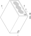
- Fig. 3A and Fig. 3B illustrate assembled schematic views of an antenna assembly according to some embodiments of the instant disclosure.
- the antenna assembly 1 is adapted to be assembled on a desktop computer 500.
- the antenna assembly 1 comprises a shielding body 10 and an antenna body 20.
- the shielding body 10 comprises a first wall 11, two first shielding walls 13, and two second shielding walls 15.
- the first wall 11 is connected to the two first shielding walls 13 and the two second shielding walls 15.
- the first wall faces an outside of the desktop computer 500. Specifically, in some embodiments, a first surface 111 of the first wall 11 is exposed from an outer surface 510 of the desktop computer 500.
- the antenna assembly 1 is on a chassis 520 of the desktop computer 500, and the antenna assembly 1 is on a surface of the chassis 520 for configuring the I/O port or on an undetachable surface of the chassis 520. Therefore, when the user disassembles the chassis of the desktop computer 500, such configuration prevents the antenna assembly 1 from being damaged. As shown in Fig.
- the antenna assembly 1 may be either disposed at the front I/O port of the desktop computer 500 or at the rear I/O of the desktop computer 500; alternatively, in some embodiments, the antenna assembly 1 may be disposed on one of the side surfaces of the desktop computer 500 as shown in Fig. 3B . It is noted that, the drawings are provided for illustrative purposes, but not limitations for the instant disclosure.
- the antenna body 20 is at the first wall 11 of the shielding body 10, and at least one portion of the antenna body 20 is connected to one of the two first shielding walls 13 or one of the two second shielding walls 15.
- the antenna body 20 operates within a frequency range of 2400 MHz to 2500 MHz or 5150 MHz to 7125 MHz, which mainly corresponds to the range of Wi-Fi specification. More specifically, in this embodiment, the antenna body 20 is at the first surface 111 of the first wall 11, that is, the outer surface of the first wall 11 in this embodiment.
- the antenna body 10 further comprises a connection portion 17.
- the connection portion 17 is a pillar structure; however, such configuration is just provided for illustrative purposes, the instant disclosure is not limited thereto.
- the two first shielding walls 13 and the two second shielding walls 15 are respectively connected to the connection portion 17.
- the two second shielding walls 15 are in parallel with each other, and the two second shielding walls 15 are respectively connected to the two first shielding walls 13.
- the shielding body 10 is a solid structure; in other words, in this embodiment, a solid portion is between the first wall 11, the two first side walls 13, the two second side walls 15, and the connection portion 17. More specifically, in this embodiment, an insulated body 10A is inside the shielding body 10.
- the insulated body may be made of, for example, plastic, rubber, acrylic, or the like.
- a shielding layer 30 which may be made of conductive material, for example, a metal layer, a graphite layer, or the like, is coated on two first side surfaces 131 of the two first shielding walls 13, two second side surfaces 151 of the two second shielding walls 15, and a surface of the connection portion 17, so that the shielding layer 30 is at least formed as the two first shielding walls 13 and the two second shielding walls 15 of the shielding body 10. More specifically, in this embodiment, upon manufacturing the antenna assembly 1, fine rough structures are formed on the surface of the first wall 11, the two first side surfaces 131, the two second side surfaces 151, and the surface of the connection portion 17 by surface scoring, acidic treatment, etching, laser engraving, electrical discharge machining, or the like. Next, electroplating or other coating techniques are applied to coat a conductive film (such as a metal film) on these surfaces to form the shielding layer 30. Furthermore, through the masking procedure, the antenna body can be formed upon performing the coating procedure.
- a conductive film such as a metal film
- the antenna assembly 1 further comprises a fixation base 18.
- the fixation base 18 is connected to the shielding body 10; the fixation base 18 and the shielding body 10 may be integrally formed as a one-piece structure or may be assembled with each other. More specifically, in some embodiments, the fixation base 18 extends from the connection portion 17.
- the fixation base 18 is adapted to be assembled with the chassis 520 of the desktop computer 500, and the shielding layer 30 is further on the surface of the fixation base 18.
- a portion of the first wall 11 has a recessed portion and a portion of one of the two second shielding walls 15 has an engaging groove 155. Therefore, the assembling of a signal feed-in wire 600 (not shown in Fig. 1 ; as shown in Fig. 4 , Fig. 5 , and Fig. 8 to Fig. 10 ) can be achieved conveniently.
- Fig. 4 illustrates a perspective view of an antenna assembly according to a second embodiment of the instant disclosure.
- Fig. 5 illustrates an exploded view of the antenna assembly of the second embodiment.
- Fig. 6A and Fig. 6B respectively illustrate cross-sectional views along the line A-A and the line B-B shown in Fig. 5 .
- the difference between the second embodiment and the first embodiment is at least that, in this embodiment, the shielding body 10 comprises a shielding housing 12 and a circuit board 20A, the circuit board 20A is assembled with the shielding housing 12, and the circuit board 20A is provided as the first wall 11 of the shielding body 10.
- the circuit board 20A and the antenna body 20 together form the radiation member to be assembled with the shielding housing 12.
- the design of the antenna body 20, the manufacture of the radiation member, and the manufacture of the shielding housing 12 can be separately, thus allowing the manufacture and design of different parts of the antenna assembly 1 can be achieved at the same time to accelerate the overall manufacturing process of the antenna assembly 1.
- Fig. 6A and Fig. 6B respectively illustrate cross-sectional views along the line A-A and the line B-B shown in Fig. 5 .
- the shielding housing 12 comprises an insulated housing 12A and a shielding layer 30.
- the shielding layer 30 encloses the insulated housing 12A. More specifically, in some embodiments, the shielding layer 30 may be an electroplating metal layer or an electroless metal layer fully covering the inner and outer surfaces of the insulated housing 12A. Therefore, according to some embodiments, the overall manufacturing costs for the antenna assembly 1 can be much cheaper, and the antenna assembly can be manufactured rapidly according to various specifications.
- the shielding housing 12 usually faces the interior of the desktop computer 500 to shield the frequency generated by the DDR5 memory so as to reduce the noises at about 6000 MHz generated by the antenna body 20.
- the shielding layer 12 comprises a connection portion 17, two first shielding walls 13, and two second shielding walls 15.
- the two first shielding walls 13 and the two second shielding walls 15 are respectively connected to the connection portion 17.
- the connection portion 17 faces the circuit board 20A, the two second shielding walls 15 are in parallel with each other and are respectively connected to the two first shielding walls 13.
- the two first shielding walls 13 may be of a symmetrical configuration or a non-symmetrical configuration.
- a receiving space R is between the connection portion 17, the two first shielding walls 13, and the two second shielding walls 15.
- the circuit board 20A is provided with two first engaging portions 119, each of the two second shielding walls 15 is provided with a second engaging portion 153, the two first engaging portions 119 extend into the receiving space R, the two second engaging portions 153 extend toward the receiving space R, and each of the first engaging portions 119 is engaged with a corresponding one of the second engaging portions 153.
- first engaging portion 119 is a hook extending upward
- second engaging portion 153 is a protruding buckle; however, such configuration is provided for illustrative purposes, not limitations to the instant disclosure.
- the structures of the first engaging portion 119 and the second engaging portion 153 may be exchanged or modified according to actual design demands.
- the shielding housing 12 further comprises a plurality of abutting members 133.
- the abutting members 133 respectively extend toward the receiving space R from the two first shielding walls 13 to abut against the circuit board 20A. Therefore, the components of the antenna assembly 1 can be assembled more closely.
- the abutting members 133 may be protrusions extending from the two first shielding walls 13 to abut against the side portion of the circuit board 20A.
- one of the two second shielding walls 15 has an engaging groove 155, the engaging groove 155 is in communication with the receiving space R, the circuit board 20A is provided with an engaging block 117, a bottom portion of one of the two first engaging portions 119 is on the engaging block 117, and one side of the engaging block 117 is correspondingly engaged with the engaging groove 115.
- a recessed portion 113 is on a surface of the circuit board 20A, the recessed portion 113 extends toward one side portion of the circuit board 20A. The shape of one end of the recessed portion 113 substantially corresponds to the shape of the engaging groove 155, and the recessed portion 155 are configured to receive and to weld to the signal feed-in wire 600.
- the shielding housing 12 further comprises a fixation base 18, the fixation base 18 is connected to the connection portion 17, and the fixation base 18 is adapted to be assembled with the chassis 520 of the desktop computer 500.
- Fig. 7 illustrates an exploded view of an antenna assembly according to a third embodiment of the instant disclosure.
- the difference between the third embodiment and the first embodiment is at least the configuration of the shielding housing 12.
- the top of the shielding housing 12 is a flat plate structure.
- the shielding housing 12 comprises a top wall 19, two first shielding walls 13, and two second shielding walls 15.
- the two first shielding walls 13 and the two second shielding walls 15 are connected to the top wall 19, respectively.
- the two first shielding walls 13 are in parallel with each other, the two second shielding walls 15 are in parallel with each other, and the two second shielding walls 15 are connected to the two first shielding walls 13, respectively.
- a receiving space R is between the top wall 19, the two first shielding walls 13, and the two second shielding walls 15.
- the circuit board 20A is provided with two first engaging portions 119
- the two second shielding walls 15 are provided with two second engaging portions 153
- the two first engaging portions 119 extend into the receiving space R
- the two second engaging portions 153 extend toward the receiving space R from inner sides of the two second shielding walls 15, and each of the first engaging portions 119 is engaged with a corresponding one of the second engaging portions 153.
- the fixation base 18 is connected to one of the two second shielding walls 14 and extends away from receiving space R; however, such configuration is provided for illustrative purposes, not limitations of the instant disclosure.
- the fixation base 18 may be connected to and extend from one of the two first shielding walls 13 or one of the two second shielding walls 15.
- the shielding housing 12 may be replaced by a metal housing.
- the antenna body 20 may be on any surface of the circuit board 20A.
- Fig. 8 illustrates an exploded view of an antenna assembly according to a fourth embodiment of the instant disclosure.
- the shielding housing 12 is a metal housing.
- the antenna assembly 1 further comprises a cover plate 40.
- the circuit board 20A and the shielding housing 12 are assembled with each other in an indirect manner; the shielding housing 12 is assembled with the cover plate 40, the circuit board 20A is on the cover plate 40, and the circuit board 20A is fixed between the shielding housing 12 and the cover plate 40.
- the cover plate 40 is an insulated member.
- the shielding housing 12 may be directly assembled on the chassis 520 of the desktop computer 500, so that the antenna body 20 on the circuit board 20A and the cover plate 40 faces the outside of the desktop computer 500.
- the antenna assembly 1 further comprises an electrical conductive film 50.
- the electrical conductive film 50 is at a portion of the circuit board 20A and a portion of the shielding housing 12, and the electrical conductive film 50 is connected to at least one portion of the antenna body 20. Therefore, the shielding housing 12 is not only provided for shielding but also for the grounding of the antenna body 20.
- Fig. 9 illustrates an exploded view of an antenna assembly according to a fifth embodiment of the instant disclosure.
- the antenna assembly 1 further comprises a pressing member 43, an assembling member 45, a bottom plate 47, and a fixation member 60.
- the shielding housing 12 further comprises two first peripheral portions 14, a second peripheral portion 16, and a fixation base 18.
- the two first peripheral portions 14 extend from the two first shielding walls 13 in a direction substantially perpendicular to the two first shielding walls 13, and the second peripheral portion 16 and the fixation base 18 extend from the two second shielding walls 15 in a direction substantially perpendicular to the two second shielding walls 15.
- the bottom plate 47 loads the circuit board 20A and is disposed above the cover plate 40.
- the assembling member 45 surrounds three sides of the circuit board 20A and fixed on the bottom plate 47.
- the shielding housing 12 covers the cover plate 40.
- the pressing member 43 is fixed on the fixation base 18 and the first peripheral portion 14.
- the fixation member 60 may be locked with the fixation base 18, so that the fixation member 60 can be prevented from being detached off the fixation base 18 and the position of the circuit board 20A can be prevented from having offset.
- one side of the assembling member 45 adjacent to the second peripheral portion 16 is provided with a washer 49 to prevent the position of the circuit board 20A from having offset.
- Fig. 10 illustrates an exploded view of an antenna assembly according to a sixth embodiment of the instant disclosure. Please refer to Fig. 10 and Fig. 9 .
- the pressing member 43, the bottom plate 47, and the washer 49 are omitted, and in this embodiment, the shielding housing 12 and the cover plate 40 are fixed with each other just through the fixation member 60.
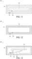
- the antenna body 20 comprises a peripheral portion 21, a radiation portion 23, a signal feed-in portion 25, and a welding portion 27.
- the peripheral portion 21 is on a periphery of a surface of the circuit board 20A and contacts one of the two first shielding walls 13 or one of the two second shielding walls 15 for grounding. In this embodiment, the peripheral portion 21 surrounds the radiation portion 23.
- the radiation portion 23 may have patterns for various Wi-Fi bands.
- the radiation portion 23 may be a monopole antenna or a dipole antenna.
- the signal feed-in portion 25 is on the radiation portion 23 and configured to be connected to a signal feed-in wire 600.
- the welding portion 27 is on the periphery portion 21 and configured to be welded with the signal feed-in wire 600.
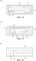
- the pattern of the antenna shown in Fig. 13 and Fig. 14 is different from the pattern of the antenna shown in Fig. 11 and Fig. 12 .
- the antenna body 20 comprises a bridging portion 29 connected between the peripheral portion 21 and the radiation portion 23.
- the peripheral portion 21 has a notch 211. It is understood that, the aforementioned patterns of the antenna body 20 are provided for illustrative purposes, not limitations to the instant disclosure. Any pattern meeting Wi-Fi bands can be provided as the pattern of the antenna body 20.
- the configuration of the antenna body 20 is different from that shown in the aforementioned embodiments.
- the antenna body 20 comprises a side edge portion 22, a radiation portion 23, a signal feed-in portion 25, and a welding portion 27.
- the side edge portion 22 is at one side of the first wall 11 and indirectly or directly connected to one of the two first shielding walls 13 or one of the two second shielding walls 15.
- the radiation portion 23 is at one side of the side edge portion 22.
- the signal feed-in portion 25 is on the radiation portion 23 and configured to be connected to a signal feed-in wire 600.
- the welding portion 27 is on the side edge portion 22 and configured to be welded with the signal feed-in wire 600.
- the antenna assembly can shield the frequency generated from the desktop computer caused by the DDR5 memory. Therefore, noises generated by the antenna body at a frequency band about of 6000 MHz can be reduced, thereby increasing the efficiency in wireless communication of the desktop computer.
- the antenna assembly 1 can shield the frequency generated from the desktop computer 500 caused by the DDR5 memory. Therefore, noises generated by the antenna body 20 at a frequency band about of 6000 MHz can be reduced, thereby increasing the efficiency in wireless communication of the desktop computer 500.
Landscapes
- Engineering & Computer Science (AREA)
- Computer Hardware Design (AREA)
- General Engineering & Computer Science (AREA)
- Physics & Mathematics (AREA)
- Electromagnetism (AREA)
- Shielding Devices Or Components To Electric Or Magnetic Fields (AREA)
- Details Of Aerials (AREA)
Applications Claiming Priority (2)
| Application Number | Priority Date | Filing Date | Title |
|---|---|---|---|
| TW111207886U TWM635704U (zh) | 2022-07-21 | 2022-07-21 | 天線總成 |
| TW111209616U TWM635802U (zh) | 2022-09-02 | 2022-09-02 | 天線總成 |
Publications (1)
| Publication Number | Publication Date |
|---|---|
| EP4325659A1 true EP4325659A1 (de) | 2024-02-21 |
Family
ID=87418913
Family Applications (1)
| Application Number | Title | Priority Date | Filing Date |
|---|---|---|---|
| EP23186046.1A Pending EP4325659A1 (de) | 2022-07-21 | 2023-07-18 | Antennenanordnung |
Country Status (3)
| Country | Link |
|---|---|
| US (1) | US12476345B2 (de) |
| EP (1) | EP4325659A1 (de) |
| JP (1) | JP3243774U (de) |
Families Citing this family (1)
| Publication number | Priority date | Publication date | Assignee | Title |
|---|---|---|---|---|
| CN119093007A (zh) * | 2023-06-06 | 2024-12-06 | 英业达科技有限公司 | 电子装置及天线组件 |
Citations (2)
| Publication number | Priority date | Publication date | Assignee | Title |
|---|---|---|---|---|
| US20170309993A1 (en) * | 2016-04-22 | 2017-10-26 | Quanta Computer Inc. | Mobile device |
| US20200014092A1 (en) * | 2018-07-05 | 2020-01-09 | Wistron Corp. | Mobile device and antenna structure therein |
Family Cites Families (3)
| Publication number | Priority date | Publication date | Assignee | Title |
|---|---|---|---|---|
| CN102790262B (zh) * | 2011-05-19 | 2014-11-05 | 光宝电子(广州)有限公司 | 天线与具有该天线的电子装置 |
| TWI578617B (zh) * | 2013-06-07 | 2017-04-11 | 富智康(香港)有限公司 | 天線組件及應用該天線組件的無線通訊裝置 |
| TWI578608B (zh) * | 2014-03-12 | 2017-04-11 | 鴻騰精密科技股份有限公司 | 天線組合及其組裝方法 |
-
2023
- 2023-07-18 EP EP23186046.1A patent/EP4325659A1/de active Pending
- 2023-07-21 US US18/356,643 patent/US12476345B2/en active Active
- 2023-07-21 JP JP2023002606U patent/JP3243774U/ja active Active
Patent Citations (2)
| Publication number | Priority date | Publication date | Assignee | Title |
|---|---|---|---|---|
| US20170309993A1 (en) * | 2016-04-22 | 2017-10-26 | Quanta Computer Inc. | Mobile device |
| US20200014092A1 (en) * | 2018-07-05 | 2020-01-09 | Wistron Corp. | Mobile device and antenna structure therein |
Also Published As
| Publication number | Publication date |
|---|---|
| US12476345B2 (en) | 2025-11-18 |
| US20240030587A1 (en) | 2024-01-25 |
| JP3243774U (ja) | 2023-09-19 |
Similar Documents
| Publication | Publication Date | Title |
|---|---|---|
| US10673142B2 (en) | Antenna module | |
| US20080139057A1 (en) | Electrical connector | |
| US20080122722A1 (en) | Chip antenna | |
| US20110044019A1 (en) | Electromagnetic shield structure, wireless device using the structure, and method of manufacturing electromagnetic shield | |
| JP5712964B2 (ja) | アンテナ装置 | |
| US9455490B2 (en) | Communication device integrally formed with antenna and mask | |
| US12476345B2 (en) | Antenna assembly | |
| US20090159329A1 (en) | Electrical Device | |
| EP1633015B1 (de) | Abdichtelement und Dichtungsanordnung für elektronische Schaltung | |
| TWI685143B (zh) | 行動裝置 | |
| US20100255893A1 (en) | Mobile communication apparatus and antenna structure | |
| CN220138696U (zh) | 天线总成 | |
| KR200307069Y1 (ko) | 굽힘 구조를 갖는 2중밴드 안테나 | |
| CN217983643U (zh) | 天线总成 | |
| JP3094771B2 (ja) | 電子・通信装置ユニット構造 | |
| US10224609B2 (en) | Antenna using conductor and electronic device therefor | |
| US12463335B2 (en) | Shield can having antenna function | |
| JP2004071629A (ja) | シールド構造およびシールド構造を有する電子機器 | |
| CN117477203A (zh) | 天线总成 | |
| KR100826840B1 (ko) | 전도성 유전체를 이용한 내장형 안테나 모듈 | |
| US10935057B2 (en) | Adapter plate for HF structures | |
| WO2020255648A1 (ja) | コネクタ | |
| TWM635704U (zh) | 天線總成 | |
| US12562495B2 (en) | Antenna assembly | |
| TWI876509B (zh) | 電子裝置及天線模組 |
Legal Events
| Date | Code | Title | Description |
|---|---|---|---|
| PUAI | Public reference made under article 153(3) epc to a published international application that has entered the european phase |
Free format text: ORIGINAL CODE: 0009012 |
|
| STAA | Information on the status of an ep patent application or granted ep patent |
Free format text: STATUS: THE APPLICATION HAS BEEN PUBLISHED |
|
| AK | Designated contracting states |
Kind code of ref document: A1 Designated state(s): AL AT BE BG CH CY CZ DE DK EE ES FI FR GB GR HR HU IE IS IT LI LT LU LV MC ME MK MT NL NO PL PT RO RS SE SI SK SM TR |
|
| STAA | Information on the status of an ep patent application or granted ep patent |
Free format text: STATUS: REQUEST FOR EXAMINATION WAS MADE |
|
| 17P | Request for examination filed |
Effective date: 20240812 |
|
| RBV | Designated contracting states (corrected) |
Designated state(s): AL AT BE BG CH CY CZ DE DK EE ES FI FR GB GR HR HU IE IS IT LI LT LU LV MC ME MK MT NL NO PL PT RO RS SE SI SK SM TR |