EP4329193A1 - Circuit récepteur - Google Patents
Circuit récepteur Download PDFInfo
- Publication number
- EP4329193A1 EP4329193A1 EP22306256.3A EP22306256A EP4329193A1 EP 4329193 A1 EP4329193 A1 EP 4329193A1 EP 22306256 A EP22306256 A EP 22306256A EP 4329193 A1 EP4329193 A1 EP 4329193A1
- Authority
- EP
- European Patent Office
- Prior art keywords
- pin
- receiver
- input
- voltage
- ground
- Prior art date
- Legal status (The legal status is an assumption and is not a legal conclusion. Google has not performed a legal analysis and makes no representation as to the accuracy of the status listed.)
- Pending
Links
Images


Classifications
-
- H—ELECTRICITY
- H03—ELECTRONIC CIRCUITRY
- H03K—PULSE TECHNIQUE
- H03K17/00—Electronic switching or gating, i.e. not by contact-making and –breaking
- H03K17/51—Electronic switching or gating, i.e. not by contact-making and –breaking characterised by the components used
- H03K17/56—Electronic switching or gating, i.e. not by contact-making and –breaking characterised by the components used by the use, as active elements, of semiconductor devices
- H03K17/687—Electronic switching or gating, i.e. not by contact-making and –breaking characterised by the components used by the use, as active elements, of semiconductor devices the devices being field-effect transistors
-
- H—ELECTRICITY
- H03—ELECTRONIC CIRCUITRY
- H03F—AMPLIFIERS
- H03F1/00—Details of amplifiers with only discharge tubes, only semiconductor devices or only unspecified devices as amplifying elements
- H03F1/26—Modifications of amplifiers to reduce influence of noise generated by amplifying elements
-
- H—ELECTRICITY
- H04—ELECTRIC COMMUNICATION TECHNIQUE
- H04B—TRANSMISSION
- H04B1/00—Details of transmission systems, not covered by a single one of groups H04B3/00 - H04B13/00; Details of transmission systems not characterised by the medium used for transmission
- H04B1/06—Receivers
- H04B1/16—Circuits
-
- H—ELECTRICITY
- H03—ELECTRONIC CIRCUITRY
- H03F—AMPLIFIERS
- H03F3/00—Amplifiers with only discharge tubes or only semiconductor devices as amplifying elements
- H03F3/04—Amplifiers with only discharge tubes or only semiconductor devices as amplifying elements with semiconductor devices only
- H03F3/08—Amplifiers with only discharge tubes or only semiconductor devices as amplifying elements with semiconductor devices only controlled by light
- H03F3/087—Amplifiers with only discharge tubes or only semiconductor devices as amplifying elements with semiconductor devices only controlled by light with IC amplifier blocks
-
- H—ELECTRICITY
- H03—ELECTRONIC CIRCUITRY
- H03F—AMPLIFIERS
- H03F3/00—Amplifiers with only discharge tubes or only semiconductor devices as amplifying elements
- H03F3/45—Differential amplifiers
- H03F3/45071—Differential amplifiers with semiconductor devices only
- H03F3/45076—Differential amplifiers with semiconductor devices only characterised by the way of implementation of the active amplifying circuit in the differential amplifier
- H03F3/45475—Differential amplifiers with semiconductor devices only characterised by the way of implementation of the active amplifying circuit in the differential amplifier using IC blocks as the active amplifying circuit
-
- H—ELECTRICITY
- H03—ELECTRONIC CIRCUITRY
- H03K—PULSE TECHNIQUE
- H03K17/00—Electronic switching or gating, i.e. not by contact-making and –breaking
- H03K17/06—Modifications for ensuring a fully conducting state
- H03K17/063—Modifications for ensuring a fully conducting state in field-effect transistor switches
-
- H—ELECTRICITY
- H03—ELECTRONIC CIRCUITRY
- H03K—PULSE TECHNIQUE
- H03K17/00—Electronic switching or gating, i.e. not by contact-making and –breaking
- H03K17/10—Modifications for increasing the maximum permissible switched voltage
- H03K17/102—Modifications for increasing the maximum permissible switched voltage in field-effect transistor switches
-
- H—ELECTRICITY
- H03—ELECTRONIC CIRCUITRY
- H03F—AMPLIFIERS
- H03F2200/00—Indexing scheme relating to amplifiers
- H03F2200/186—Indexing scheme relating to amplifiers the ground, reference potential being controlled
-
- H—ELECTRICITY
- H03—ELECTRONIC CIRCUITRY
- H03F—AMPLIFIERS
- H03F2200/00—Indexing scheme relating to amplifiers
- H03F2200/189—Indexing scheme relating to amplifiers the ground, reference or shield potential difference between different chips being controlled
-
- H—ELECTRICITY
- H03—ELECTRONIC CIRCUITRY
- H03F—AMPLIFIERS
- H03F2203/00—Indexing scheme relating to amplifiers with only discharge tubes or only semiconductor devices as amplifying elements covered by H03F3/00
- H03F2203/45—Indexing scheme relating to differential amplifiers
- H03F2203/45511—Indexing scheme relating to differential amplifiers the feedback circuit [FBC] comprising one or more transistor stages, e.g. cascaded stages of the dif amp, and being coupled between the loading circuit [LC] and the input circuit [IC]
Definitions
- the present disclosure relates to receiver circuits, and in particular to receiver circuits for processing infrared signals received at a photo-diode.
- a receiver circuit comprising:
- the MOSFET and the amplifier can improve the performance of the receiver circuit with respect to ground noise injection.
- the MOSFET is a PMOS MOSFET.
- the MOSFET is an NMOS MOSFET.
- the receiver circuit may further include a reference-voltage-source-source that is configured to provide a reference voltage to another input terminal of the amplifier.
- the receiver circuit further comprises:
- the internal-node is galvanically connected to the input-pin by a bond wire.
- the input-pin is configured to receive a current signal from a sensor.
- the senor comprises a photo-diode.
- an integrated circuit comprising any receiver circuit disclosed herein.
- a system comprising:
- the senor comprises a photo-diode.
- the system is a battery management system.
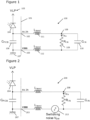
- Figure 1 shows an example of a receiver circuit 100.
- the receiver circuit is provided on an integrated circuit (IC), a boundary of which is shown with a dashed line 101 in Figure 1 .
- IC integrated circuit
- Two of the pins of the IC are shown in Figure 1 : an input-pin, rx_in, 102 and a ground-pin, vssa, 103.
- the receiver circuit 100 is for an infra red (IR) communication system, in this example an IR communication system for a battery management system (BMS). Such an IR communication system may be a serial IR system.
- IR infra red
- BMS battery management system
- Such an IR communication system may be a serial IR system.
- a photo-diode 104 is shown connected to the input-pin, rx_in, 102. The photo-diode 104 receives an IR communication signal from a corresponding IR transmitter.
- the photo-diode 104 is connected to a low power voltage source (VLP) 105.
- VLP low power voltage source
- C PCB capacitance
- 106 connected in series between the input-pin, rx_in, 102 and a printed circuit board (PCB) ground 107.
- the ground-pin, vssa, 103 of the IC is also connected to the PCB ground 107.
- This capacitance, C PCB , 106 represents the parasitic capacitance of the PCB to which the IC is connected.
- a receiver-input-node 108 is indicated in the figure.
- the inductance of a bond wire, L bond , 111 is shown connected between the input-pin, rx_in, 102 and the receiver-input-node 108.
- An input-resistor 109, R IN , 109 and an input-capacitor, CIN, 110 are shown connected in parallel between the receiver-input-node 108 and the ground-pin, vssa, 103 (via another bond wire, L bond , 112).
- the input-resistor 109, R IN , 109 and the input-capacitor, C IN , 110 are included to represent the input impedance of the receiver.
- the receiver circuit 100 includes additional components for providing a receiver-output-signal, rx_out.
- ground noise is generated inside the integrated circuit due to transient current consumption flowing through the bond wires, L bond , 111, 112. Current consumption can come from blocks sharing the same ground.
- Figure 2 shows the receiver circuit of Figure 1 that will be used to describe the effects of such ground noise.
- Figure 2 that have already been described with reference to Figure 1 have been given corresponding reference numbers in the 200 series and will not necessarily be described again here.
- a switching noise voltage source, V SW , 213 is shown to model a perturbation induced by other operating blocks (with conducted current or substrate noise injection (SNI)) sharing the same ground.
- the ground noise that is identified above, and that is modelled in Figure 2 as the switching noise voltage source, V SW , 213, can generate tens of mV of noise with respect to PCB ground 207 on the local IC grounds (ground-pin, vssa, 203 in Figure 2 ). Therefore, the voltage at the receiver-input-node 208 with respect to PCB ground 207 is modulated by this same ground noise level.
- the ground noise can be "seen” by the receiver at the receiver-input-node 208 as an input signal depending on its amplitude and frequency. Therefore, this unintended input current signal at the receiver-input-node 208 can generate an unintended (and undesirable) receiver output signal, rx_out, which can prevent the receiver from properly decoding the expected input signal that is provided by the photo-diode 204 (or any other external sensor, depending upon the communication system).
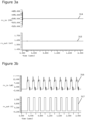
- Figures 3a and 3b illustrate simulation results for the receiver of Figure 1 ; that is, one that doesn't have any noise.
- Figure 3a shows a simulation when there is no communication (that is, the photo-diode that is shown in Figure 1 does not receive an IR communication signal).
- the upper plot of Figure 3a shows the current 314 at the input-pin, rx_in.
- the lower plot of Figure 3a shows the voltage 315 of the receiver-output-signal, rx_out. As expected, there is no noise present in either of the plots of Figure 3a .
- Figure 3b shows a simulation when there is high speed communication (that is, the photo-diode that is shown in Figure 1 receives an IR communication signal).
- the upper plot of Figure 3b shows the current 316 at the input-pin, rx_in; and the lower plot of Figure 3b shows the voltage 317 of the receiver-output-signal, rx_out.
- the receiver-output-signal, rx_out, 317 provides a good representation of the input-signal that is provided by the photo-diode.
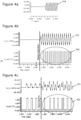
- Figures 4a, 4b and 4c illustrate simulation results for the receiver of Figure 2 ; that is, one that has the switching noise modelled by a switching noise voltage source, V SW .
- Figure 4a shows a simulation of the voltage provided by the switching noise voltage source, V SW , 418 which in this example has a value of 36 mVpp (millivolts, peak to peak amplitude). As can be seen from Figure 4a , the noise is injected after 1 ⁇ s.
- Figure 4b shows a simulation when there is no communication (that is, the photo-diode that is shown in Figure 2 does not receive an IR communication signal).
- the upper plot of Figure 4b shows the current 419 at the input-pin, rx_in.
- the lower plot of Figure 4b shows the voltage 420 of the receiver-output-signal, rx_out.
- the noise injected after 1 ⁇ s is processed by the receiver such that it translates into a receiver-output-signal, rx_out, 420 that incorrectly indicates that communication data has been received by the photo-diode. That is, when Rx_in is perturbated by switching noise when there is no communication, the receiver is affected such that it outputs the wrong message.
- Figure 4c shows a simulation when there is high speed communication (that is, the photo-diode that is shown in Figure 2 receives an IR communication signal).
- the upper plot of Figure 4c shows the current 421 at the input-pin, rx_in; and the lower plot of Figure 4c shows the voltage 422 of the receiver-output-signal, rx_out.
- the noise injected after 1 ⁇ s degrades the quality of the receiver-output-signal, rx_out, 422. That is, when Rx_in is perturbated by switching noise when there is communication, the receiver is also affected such that it outputs the wrong message.
- Examples of the present disclosure can significantly improve high-speed current mode communication and the impact of receiver ground noise on the sensitivity of the receiver.
- Such examples can improve immunity from this noise, which is equivalent to an input current signal in current mode communication, especially where the receiver input stage is low impedance. Due to this noise immunity improvement, a receiver detection threshold can then be set to a lower current level and therefore can allow communication over longer distances between an emitter and the receiver (e.g. infrared communication with photo-diodes).
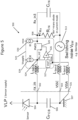
- Figure 5 illustrates an example embodiment of a receiver circuit 500 according to the present disclosure.
- Features of Figure 5 that are also illustrated in an earlier drawing are given corresponding reference numbers in the 500 series and will not necessarily be described again here.
- the receiver circuit 500 has an input-pin, rx_in, 502 and a receiver-input-node, Rx_in3, 508 that are the same way as those described with reference to Figures 1 and 2 .
- the IC that includes the receiver circuit 500 has two ground pins: a first-ground-pin, VSSC, 503 and a second-ground-pin, VSSA, 531.
- the first-ground-pin, VSSC, 503 is a reference pin for communication blocks in the IC, including the receiver circuit 500.
- the second-ground-pin, VSSA, 531 is a reference pin for other blocks in the IC.
- Providing two separate ground-pins 503, 531 in this way can beneficially reduce the ground noise that is experienced at the ground-pin (VSSC, 503) for the receiver circuit 500. Nonetheless, as will be discussed below with reference to Figure 9 , in other examples the IC may have only one ground-pin.
- the receiver circuit 500 also includes an internal-node, Rx_in2, 524 that is connected to the input-pin, rx_in, 502.
- Rx_in2 an internal-node
- the internal-node, Rx_in2, 524 is galvanically connected to the input-pin, rx_in, 502.
- the package may not require bond wires and therefore the internal-node, Rx_in2, 524 does not necessarily need to be galvanically connected to the input-pin, rx_in, 502.
- the receiver circuit includes additional components (when compared with Figure 1 ), that are shown in box 523 in Figure 5 , such that the internal-node, Rx_in2, 524 is a low impedance node that is connected to the sensor output (that is, the input-pin, rx_in, 502 of the IC that receives the output signal from the sensor - in this example the photo-diode 504).
- the internal-node, Rx_in2, 524 is not modulated by the switching noise voltage source, V SW , 513.
- the additional components 523 include a metal-oxide-semiconductor field-effect transistor (MOSFET).
- MOSFET metal-oxide-semiconductor field-effect transistor
- Figure 5 a PMOS MOSFET 525 is shown.
- Figure 8 illustrates how an NMOS MOSFET can be used instead.
- the PMOS MOSFET 525 has a conduction channel (between it's source and it's drain, as it known in the art) that is connected in series between the internal-node, Rx_in2, 524 and the receiver-input-node, Rx_in3, 508.
- the PMOS MOSFET 525 also has a gate terminal, the voltage at which sets the conductivity of the conduction channel.
- the additional components 523 in this example also include an amplifier 526.
- the amplifier 526 has an input terminal that is connected to the internal-node, Rx_in2, 524.
- the amplifier 526 has an output terminal that provides a voltage control signal to the gate terminal of the PMOS MOSFET 525 such that the voltage at the internal-node, Rx_in2, 524 with respect to the first-ground-pin, VSSC, 503 is constant. In this way, any "ground” switching noise voltage will not cause a significant current to be received at the input-pin, rx_in, 502 from the parasitic capacitance, CPCB, 506.
- the additional components 523 also include: a reference-voltage-source 527, a first-current-source, 10, 529 and a second-current-source, 10, 530.
- the reference-voltage-source 527 provides a voltage of Vref to another input terminal of the amplifier 526. As shown in Figure 5 , in this example, the reference-voltage-source 527 is provided with respect to the voltage on the second-ground-pin, VSSA, 531.
- the receiver circuit 500 is configured to process a signal at the receiver-input-node 508 with respect to a voltage on the first-ground-pin, VSSC, 503.
- the value of Vref can be Vsir, where Vsir is the voltage provided by a serial infrared power supply. Vsir can be 1.5V with respect to vssa, in some examples.
- Vref does not affect the functionality of the receiver circuit 500, as long as Vref is larger than rx_in3 voltage (receiver input voltage). This is important for guaranteeing that the PMOS MOSFET 525 (pass device) has more than 100-200 mV drop out voltage (VDS)
- the first-current-source, 10, 529 is connected between a supply-voltage-terminal, Vsupply, and the internal-node, Rx_in2, 524. Therefore, the first-current-source, 10, 529 provides a current to one end of the conduction channel of the PMOS MOSFET 525 (the source of the PMOS MOSFET 525 in Figure 5 ).
- the second-current-source, 10, 530 is connected between a ground-pin (in this example the second-ground-pin, VSSA, 531) and the receiver-input-node, Rx_in3, 508.
- the second-current-source, 10, 530 provides a current to the other end of the conduction channel of the PMOS MOSFET 525 (the drain of the PMOS MOSFET 525 in Figure 5 ).
- the first-current-source, 10, 529 and the second-current-source, 10, 530 are provided to ensure that the PMOS MOSFET 525 is correctly biased, even when the photo-diode 504 does not receive any IR light and therefore does not provide a sensed current signal, such that the PMOS MOSFET 525 is always active and can be appropriately operated such that the current through it's conduction channel can be controlled.
- the additional components 523 create a new low impedance node (the internal-node, Rx_in2, 524) that is connected to the sensor output (via the input-pin, rx_in, 502) and referenced to a noise free ground (the second-ground-pin, VSSA, 531) while the receiver ground is connected to the communication ground (the first-ground-pin, VSSC, 503) which can be noisy due to current consumption of other communication blocks that are also connected to the same ground.
- the internal-node, Rx_in2, 524 that is connected to the sensor output (via the input-pin, rx_in, 502) and referenced to a noise free ground (the second-ground-pin, VSSA, 531) while the receiver ground is connected to the communication ground (the first-ground-pin, VSSC, 503) which can be noisy due to current consumption of other communication blocks that are also connected to the same ground.
- the voltage at the input-pin, rx_in, 502 with respect to pcb_ground 507 is still noisy but it does not generate a current input signal at the receiver output because the drain impedance of the PMOS MOSFET 525 is high enough to avoid or reduce current coupling.
- Figures 6a and 6b illustrate simulation results for the receiver circuit of Figure 5 , but without the switching noise voltage source, V SW .
- Figures 7a, 7b and 7c illustrate simulation results for the receiver circuit of Figure 5 with the switching noise voltage source, V SW .
- Figure 6a shows a simulation when there is no communication (that is, the photo-diode that is shown in Figure 5 does not receive an IR communication signal).
- the upper plot of Figure 6a shows the current 632 at the input-pin, rx_in.
- the lower plot of Figure 6a shows the voltage 633 of the receiver-output-signal, rx_out.
- there is no noise present in either of the plots of Figure 6a .
- the inclusion of the additional components of Figure 5 does not affect the voltage 633 of the receiver-output-signal, rx_out.
- Figure 6b shows a simulation when there is high speed communication (that is, the photo-diode that is shown in Figure 5 receives an IR communication signal).
- the upper plot of Figure 6b shows the current 634 at the input-pin, rx_in; and the lower plot of Figure 6b shows the voltage 635 of the receiver-output-signal, rx_out.
- the inclusion of the additional components of Figure 5 cause the current 634 at the input-pin, rx_in, to have a slightly different shape but that the receiver-output-signal, rx_out, 635 is unaffected. That is, the inclusion of the additional components in Figure 5 does not degrade the performance of the receiver circuit when there is no noise present.
- Figure 7a shows a simulation of the voltage provided by the switching noise voltage source, Vsw, 736.
- the noise in Figure 7a is injected after 1 ⁇ s (purely as an example).
- Figure 7b shows a simulation when there is no communication (that is, the photo-diode that is shown in Figure 5 does not receive an IR communication signal).
- the upper plot of Figure 7b shows the current 737 at the input-pin, rx_in, which includes the noise that is injected by the switching noise voltage source, V SW , 736.
- the lower plot of Figure 7b shows the voltage 738 of the receiver-output-signal, rx_out.
- the noise injected is not present in the receiver-output-signal, rx_out, 738. That is, despite the rx_in perturbation due to switching noise when there is no communication, there is no impact on rx_out. Therefore, advantageously the additional components of Figure 5 have improved the performance of the receiver circuit with respect to ground noise injection.
- Figure 7c shows a simulation when there is high speed communication (that is, the photo-diode that is shown in Figure 5 receives an IR communication signal).
- the upper plot of Figure 7c shows the current 739 at the input-pin, rx_in; the middle plot of Figure 7c shows the voltage 740 of the receiver-output-signal, rx_out; and the lower plot of Figure 7c shows the voltage at the node in the circuit where the noise is injected.
- the lower plot in Figure 7c is included to show that there is indeed noise in the system, even though it is not visible in the receiver-output-signal, rx_out, 740.
- the noise injected after 1 ⁇ s does not degrade the quality of the signal at the input-pin, rx_in, 739 or the receiver-output-signal, rx_out, 740. Since no switching noise is visible on rx_in current, the receiver circuit can correctly generate the message communication (rx_out).
- Figure 8 illustrates another example embodiment of a receiver circuit 800 according to the present disclosure.
- the receiver circuit of Figure 8 is very similar to the one of Figure 5 .
- an NMOS MOSFET 825 is used instead of the PMOS MOSFET of Figure 5 .
- the first-current-source, 10, 829 and the second-current-source, 10, 830 are reversed in order to provide the correct biasing for the NMOS MOSFET 825. Therefore, the first-current-source, 10, 829 is connected between a supply-voltage-terminal, Vsupply, and the receiver-input-node, Rx_in3, 808. In this way, the first-current-source, 10, 829 provides a current to one end of the conduction channel of the NMOS MOSFET 825 (the drain of the NMOS MOSFET 825 in Figure 8 ).
- the second-current-source, 10, 830 is connected between a ground-pin (in this example the second-ground-pin, VSSA, 831 and the internal-node, Rx_in2, 824. Therefore, the second-current-source, 10, 830 provides a current to the other end of the conduction channel of the NMOS MOSFET 825 (the source of the NMOS MOSFET 825 in Figure 8 ).
- Figure 9 illustrates a yet further example embodiment of a receiver circuit 900 according to the present disclosure.
- the receiver circuit of Figure 9 is similar to the one of Figure 5 .
- Features of Figure 9 that have already been described with reference to Figure 5 will not necessarily be described again here.
- the reference-voltage-source 927 is provided with respect to the voltage on the first-ground-pin, VSSC, 903. That is, the first-ground-pin, VSSC, 903 is the reference-pin for the reference-voltage-source 927 and also for the receiver circuit 900. In this way, the receiver circuit is configured to process a signal at the receiver-input-node 908 with respect to a voltage on the first-ground-pin, VSSC, 903.
- the additional components 923 of Figure 9 create the new low impedance node (the internal-node, Rx_in2, 524) that is connected to the sensor output and in this example is referenced to VSSC ground (the first-ground-pin 903).
- VSSC ground the first-ground-pin 903
- multiple ground pins do not exist and therefore it is beneficial that the additional components 923 of this example can function adequately using only one ground pin (the first-ground-pin 903) for all IC functions.
- NMOS MOSFET can be used instead of the PMOS MOSFET 925 that is shown in Figure 9 .
- NMOS MOSFET 825 of Figure 8 can be used instead of the PMOS MOSFET 525 of Figure 5 .
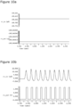
- Figures 10a and 10b illustrate simulation results for the receiver circuit of Figure 9 , but without the switching noise voltage source, V SW .
- Figures 10a and 10b are very similar to Figures 6a and 6b , and will not be described in any detail here.
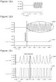
- Figures 11a, 11b and 11c illustrate simulation results for the receiver circuit of Figure 9 with the switching noise voltage source, V SW .
- Figures 11a, 11b and 11c are very similar to Figures 7a, 7b and 7c .
- Examples disclosed herein include circuitry that is added in series between a current mode receiver input pin and receiver input stage (which can be a trans-diode connected MOS for current communication, but not limited to this) that allows the receiver to operate with noise on its ground (without generating an unintended signal on its output).
- This circuitry can artificially create a new low impedance node connected to the sensor output (Integrated Circuit: IC input pin) that is not modulated by IC internal ground noise used to ground the receiver. Therefore, the receiver input stage current is much less modulated by it's ground noise, resulting in the processing of only the current signal generated by the external sensor (e.g. photo-diode). It can enable communication over longer distances between the emitter and receiver because the receiver input current detection threshold can be set to a lower level without the risk of detecting an unwanted noise signal.
- the receivers of embodiments of the present disclosure can be current mode receivers, rather that voltage mode (that can include a high impedance differential amplifier). Therefore, applications that use a photo-diode as a sensor can be particularly well-suited to embodiments of the present disclosure because the useful information that is provided by the photo-diode is provided as a current. Such receivers of the present disclosure can provide good ground noise isolation and can also occupy relative small areas on the die.
- the set of instructions/method steps described above are implemented as functional and software instructions embodied as a set of executable instructions which are effected on a computer or machine which is programmed with and controlled by said executable instructions. Such instructions are loaded for execution on a processor (such as one or more CPUs).
- processor includes microprocessors, microcontrollers, processor modules or subsystems (including one or more microprocessors or microcontrollers), or other control or computing devices.
- a processor can refer to a single component or to plural components.
- the set of instructions/methods illustrated herein and data and instructions associated therewith are stored in respective storage devices, which are implemented as one or more non-transient machine or computer-readable or computer-usable storage media or mediums.
- Such computer-readable or computer usable storage medium or media is (are) considered to be part of an article (or article of manufacture).
- An article or article of manufacture can refer to any manufactured single component or multiple components.
- the non-transient machine or computer usable media or mediums as defined herein excludes signals, but such media or mediums may be capable of receiving and processing information from signals and/or other transient mediums.
- Example embodiments of the material discussed in this specification can be implemented in whole or in part through network, computer, or data based devices and/or services. These may include cloud, internet, intranet, mobile, desktop, processor, look-up table, microcontroller, consumer equipment, infrastructure, or other enabling devices and services. As may be used herein and in the claims, the following non-exclusive definitions are provided.
- one or more instructions or steps discussed herein are automated.
- the terms automated or automatically mean controlled operation of an apparatus, system, and/or process using computers and/or mechanical/electrical devices without the necessity of human intervention, observation, effort and/or decision.
- any components said to be coupled may be coupled or connected either directly or indirectly.
- additional components may be located between the two components that are said to be coupled.
Landscapes
- Engineering & Computer Science (AREA)
- Power Engineering (AREA)
- Computer Networks & Wireless Communication (AREA)
- Signal Processing (AREA)
- Amplifiers (AREA)
Priority Applications (3)
| Application Number | Priority Date | Filing Date | Title |
|---|---|---|---|
| EP22306256.3A EP4329193A1 (fr) | 2022-08-25 | 2022-08-25 | Circuit récepteur |
| CN202310817056.5A CN117639815A (zh) | 2022-08-25 | 2023-07-05 | 接收器电路 |
| US18/451,212 US12418286B2 (en) | 2022-08-25 | 2023-08-17 | Receiver circuit |
Applications Claiming Priority (1)
| Application Number | Priority Date | Filing Date | Title |
|---|---|---|---|
| EP22306256.3A EP4329193A1 (fr) | 2022-08-25 | 2022-08-25 | Circuit récepteur |
Publications (1)
| Publication Number | Publication Date |
|---|---|
| EP4329193A1 true EP4329193A1 (fr) | 2024-02-28 |
Family
ID=83271520
Family Applications (1)
| Application Number | Title | Priority Date | Filing Date |
|---|---|---|---|
| EP22306256.3A Pending EP4329193A1 (fr) | 2022-08-25 | 2022-08-25 | Circuit récepteur |
Country Status (3)
| Country | Link |
|---|---|
| US (1) | US12418286B2 (fr) |
| EP (1) | EP4329193A1 (fr) |
| CN (1) | CN117639815A (fr) |
Citations (3)
| Publication number | Priority date | Publication date | Assignee | Title |
|---|---|---|---|---|
| US5929434A (en) * | 1997-08-13 | 1999-07-27 | Rockwell Science Center, Llc | Ultra-low noise high bandwidth interface circuit for single-photon readout of photodetectors |
| US6696887B2 (en) * | 2001-09-27 | 2004-02-24 | Matthew S. Taubman | Transistor-based interface circuitry |
| US20110180692A1 (en) * | 2010-01-27 | 2011-07-28 | Hitachi, Ltd. | Optical receiver circuit |
Family Cites Families (3)
| Publication number | Priority date | Publication date | Assignee | Title |
|---|---|---|---|---|
| US4529947A (en) | 1979-03-13 | 1985-07-16 | Spectronics, Inc. | Apparatus for input amplifier stage |
| FR2915833B1 (fr) * | 2007-05-04 | 2010-03-12 | Thales Sa | Detecteur matriciel d'impulsions laser avec sommation rapide. |
| US9209221B2 (en) * | 2012-07-24 | 2015-12-08 | Forza Silicon Corporation | BDI IR readout circuit using pinned photodiode as integration node |
-
2022
- 2022-08-25 EP EP22306256.3A patent/EP4329193A1/fr active Pending
-
2023
- 2023-07-05 CN CN202310817056.5A patent/CN117639815A/zh active Pending
- 2023-08-17 US US18/451,212 patent/US12418286B2/en active Active
Patent Citations (3)
| Publication number | Priority date | Publication date | Assignee | Title |
|---|---|---|---|---|
| US5929434A (en) * | 1997-08-13 | 1999-07-27 | Rockwell Science Center, Llc | Ultra-low noise high bandwidth interface circuit for single-photon readout of photodetectors |
| US6696887B2 (en) * | 2001-09-27 | 2004-02-24 | Matthew S. Taubman | Transistor-based interface circuitry |
| US20110180692A1 (en) * | 2010-01-27 | 2011-07-28 | Hitachi, Ltd. | Optical receiver circuit |
Also Published As
| Publication number | Publication date |
|---|---|
| CN117639815A (zh) | 2024-03-01 |
| US20240072794A1 (en) | 2024-02-29 |
| US12418286B2 (en) | 2025-09-16 |
Similar Documents
| Publication | Publication Date | Title |
|---|---|---|
| US8050651B2 (en) | Detector, RF circuit with detector, and mobile device with RF circuit | |
| JP5074500B2 (ja) | 改善された性能を有するn−チャネルesdクランプ | |
| CN102904556B (zh) | 高侧开关 | |
| CN106611209B (zh) | 安全电子芯片 | |
| US20150123628A1 (en) | Apparatus and Method for a Voltage Regulator with Improved Power Supply Reduction Ratio (PSRR) with Reduced Parasitic Capacitance on Bias Signal Lines | |
| JPH07264042A (ja) | 高速インタフェース回路 | |
| US8410818B1 (en) | High speed communication interface with an adaptive swing driver to reduce power consumption | |
| US7940092B2 (en) | Gate driver circuit for H bridge circuit | |
| JP2017529791A (ja) | 高速dc結合通信のための共通ゲート増幅器 | |
| CN103036549B (zh) | Rf开关电路、rf开关以及用于切换rf信号的方法 | |
| US7138804B2 (en) | Automatic transmission line pulse system | |
| US11187731B2 (en) | Power glitch signal detection circuit, security chip and electronic apparatus | |
| TW391062B (en) | Semiconductor integrated circuit | |
| WO2021196958A1 (fr) | Circuit d'isolation capacitif, module d'interface, puce et système | |
| US12418286B2 (en) | Receiver circuit | |
| US20140339894A1 (en) | Pre-emphasis circuit | |
| US20110171906A1 (en) | Communication cell for an integrated circuit, chip comprising said communication cell, electronic system including the chip, and test apparatus | |
| US20240113710A1 (en) | Very Low Voltage I/O Circuit And Method For Screening Defects | |
| CN104885225A (zh) | 晶体管放大器级内信号采样的集成 | |
| US10748890B2 (en) | Negative voltage tolerant IO circuitry for IO pad | |
| WO2016125035A1 (fr) | Mise en œuvre d'un amplificateur de transimpédance optique basé sur un onduleur amélioré à cmos | |
| CN108023579A (zh) | 使用原生晶体管的电源检测电路及检测功率的方法 | |
| CN116401192B (zh) | 一种检测电路及终端设备 | |
| CN115940623B (zh) | 电磁噪声隔离方法及装置、存储介质及电子装置 | |
| CN111027384A (zh) | 指纹识别检测电路、检测方法及显示装置 |
Legal Events
| Date | Code | Title | Description |
|---|---|---|---|
| PUAI | Public reference made under article 153(3) epc to a published international application that has entered the european phase |
Free format text: ORIGINAL CODE: 0009012 |
|
| STAA | Information on the status of an ep patent application or granted ep patent |
Free format text: STATUS: THE APPLICATION HAS BEEN PUBLISHED |
|
| AK | Designated contracting states |
Kind code of ref document: A1 Designated state(s): AL AT BE BG CH CY CZ DE DK EE ES FI FR GB GR HR HU IE IS IT LI LT LU LV MC MK MT NL NO PL PT RO RS SE SI SK SM TR |
|
| STAA | Information on the status of an ep patent application or granted ep patent |
Free format text: STATUS: REQUEST FOR EXAMINATION WAS MADE |
|
| 17P | Request for examination filed |
Effective date: 20240828 |
|
| RBV | Designated contracting states (corrected) |
Designated state(s): AL AT BE BG CH CY CZ DE DK EE ES FI FR GB GR HR HU IE IS IT LI LT LU LV MC MK MT NL NO PL PT RO RS SE SI SK SM TR |