EP4330842B1 - Module médico-légal et système intégré - Google Patents
Module médico-légal et système intégré Download PDFInfo
- Publication number
- EP4330842B1 EP4330842B1 EP22725414.1A EP22725414A EP4330842B1 EP 4330842 B1 EP4330842 B1 EP 4330842B1 EP 22725414 A EP22725414 A EP 22725414A EP 4330842 B1 EP4330842 B1 EP 4330842B1
- Authority
- EP
- European Patent Office
- Prior art keywords
- data
- commitment
- embedded system
- key
- processor
- Prior art date
- Legal status (The legal status is an assumption and is not a legal conclusion. Google has not performed a legal analysis and makes no representation as to the accuracy of the status listed.)
- Active
Links
Images





Classifications
-
- G—PHYSICS
- G06—COMPUTING OR CALCULATING; COUNTING
- G06F—ELECTRIC DIGITAL DATA PROCESSING
- G06F21/00—Security arrangements for protecting computers, components thereof, programs or data against unauthorised activity
- G06F21/60—Protecting data
- G06F21/64—Protecting data integrity, e.g. using checksums, certificates or signatures
-
- G—PHYSICS
- G06—COMPUTING OR CALCULATING; COUNTING
- G06F—ELECTRIC DIGITAL DATA PROCESSING
- G06F21/00—Security arrangements for protecting computers, components thereof, programs or data against unauthorised activity
- G06F21/50—Monitoring users, programs or devices to maintain the integrity of platforms, e.g. of processors, firmware or operating systems
-
- G—PHYSICS
- G06—COMPUTING OR CALCULATING; COUNTING
- G06F—ELECTRIC DIGITAL DATA PROCESSING
- G06F21/00—Security arrangements for protecting computers, components thereof, programs or data against unauthorised activity
- G06F21/50—Monitoring users, programs or devices to maintain the integrity of platforms, e.g. of processors, firmware or operating systems
- G06F21/57—Certifying or maintaining trusted computer platforms, e.g. secure boots or power-downs, version controls, system software checks, secure updates or assessing vulnerabilities
Definitions
- Various embodiments relate to a forensics module, an embedded system and an ATM.
- KRITIS Critical infrastructures
- IT systems information technology systems
- Components of these IT systems include routers, industrial control systems, medical devices, and ATMs.
- US 10 079 842 B1 describes a block-level forensic service to detect malicious activity on logs.
- EP 3 798 883 A1 describes a digital forensics module that identifies forensic-specific metadata of the computing device from a plurality of system metadata of the computing device based on predetermined rules, wherein the forensic-specific metadata is used to detect suspicious digital activities.
- CPS cyber-physical system
- a forensic image of the suspected tampered firmware (also referred to as a firmware image) can be extracted, and this firmware image can be emulated and examined in a suitable environment.
- the tampered firmware clearly displays the original firmware and additional malicious code.
- a forensics module is provided, with which an embedded system can be extended, for example, and which extracts the forensic image and provides it in such a way that the requirements of the parties involved are met as much as possible.
- an emulation system for emulating an embedded system is provided, by means of which the forensic image can be examined as efficiently and authentically as possible.
- the timely processing of an attack on an embedded system is simplified, e.g., with greater efficiency and/or greater effectiveness. This improves the clearance rate of such attacks and thus also enables the improvement of crime prevention. This results in a significant Potential for protecting critical infrastructure and thus increasing security of supply. It can also improve police threat response and increase crime prevention through faster and more accurate information gathering.
- the state of an entity can be understood as the totality of information that fully describes the variable (e.g., time-dependent) properties of the entity.
- the actual state of the entity can be understood as the actual or sensorily detectable state of the entity at a given point in time.
- the desired state of the entity can be understood as the desired state, i.e., a specification.
- Control can be understood as an intentional influencing of the current state (also referred to as the actual state) of the entity.
- the current state can be changed according to the specification (also referred to as the desired state), e.g., by changing one or more operating parameters (then also referred to as manipulated variables) of the entity, e.g., by means of an actuator.
- a fieldbus communication protocol can be used for communication via a fieldbus.
- a USB communication protocol can be used for communication via a universal serial bus (USB).
- USB universal serial bus
- another communication protocol can also be used, which could, for example, be proprietary.
- the interface coupled to the communication infrastructure may be configured to transmit the data according to the communication protocol, for example to transmit, or at least send, or at least generate a message comprising the data according to the communication protocol.
- a system-internal bus system may be configured to provide communication between the components of an EGS.
- the system-internal bus system may, for example, comprise a processor-internal bus and a processor-external bus.
- the system-internal bus system may comprise or be formed from a fieldbus.
- the fieldbus may be configured as a network for distributed real-time communication, e.g., via a message-based communication protocol.
- the order and priority of a plurality of messages sent and/or received via the fieldbus is defined by the fieldbus communication protocol.
- Such a fieldbus communication protocol may be configured for distributed real-time control, e.g., standardized as International Electrotechnical Commission (IEC) 61158 (title "Digital data communications for measurement and control - Fieldbus for use in industrial control systems," e.g., in the version dated May 2, 2017).
- IEC International Electrotechnical Commission
- a system-external network described herein can, for example, be, depending on its range, a local network (e.g., a Local Area Network (LAN), a Wireless LAN (WLAN), or a Personal Area Network (PAN), such as a Wireless PAN (WPAN), such as a Bluetooth network) or a non-local network (e.g., a Metropolitan Area Network (MAN), a Wide Area Network (WAN), or a Global Area Network (GAN)) or be formed from it.
- LAN Local Area Network
- WLAN Wireless LAN
- PAN Personal Area Network
- WPAN Wireless PAN
- WLAN Wireless PAN
- Bluetooth network such as a Bluetooth network
- non-local network e.g., a Metropolitan Area Network (MAN), a Wide Area Network (WAN), or a Global Area Network (GAN)
- the network can, for example, differentiated according to transmission type, have a radio network (also referred to as a wireless network or cable-free network), such as a mobile radio network, or have a wired network or be formed from it.
- the network can, for example, also have a cellular radio network (e.g. a WLAN of the IEEE 802.11 type in ad hoc mode, a Bluetooth network or another cellular mobile radio network) or be formed from it, for example according to a mobile radio standard of the third generation (3G), fourth generation (4G), fifth generation (5G) or LTE (also referred to as 3.9G).
- the network can also have several interconnected sub-networks of different types.
- processor can be understood as any type of entity that allows the processing of data or (e.g., data-representing) signals.
- the data or signals can, for example, be processed according to at least one (i.e., one or more) specific function performed by the processor.
- components of a processor include: an analog circuit, a digital circuit, a mixed-signal circuit, a logic circuit, a microprocessor (e.g., in ARM architecture), a central processing unit (CPU), a graphics processing unit (GPU), a digital signal processor (DSP), a programmable gate array (FPGA), an integrated circuit, or any combination thereof.
- a microprocessor in ARM architecture is also referred to herein as an ARM processor or ARM for short. Any other type of implementation of the respective functions, which are described in more detail below, can also be understood as a processor or logic circuit. It should be understood that one or more of the processes and/or acts described in detail herein may be executed (e.g., implemented) by a processor through one or more specific functions performed by the processor. Similarly, a process or act described herein may be implemented by means of code segments configured, when executed by the processor, to cause the processor to perform the process or act.
- a data storage device may be a volatile or non-volatile data storage device.
- a non-volatile data storage device include, or may be formed from, a hard disk, a semiconductor memory, such as a read-only memory, a non-volatile random access memory (also referred to as NVRAM - "non-volatile random access memory"), and/or a flash memory (also referred to as flash for short).
- the read-only memory also referred to as ROM
- ROM may For example, it can be a programmable ROM or an erasable programmable ROM (also called EPROM).
- the volatile data storage can be, for example, a volatile random access memory.
- a cryptographic key (also simply referred to as a key) is understood to be information (e.g. a character string) that parameterizes the cryptographic process (e.g. its algorithm) and thus influences its output (e.g. independent of the input).
- a sensor can be understood as a component that is configured to detect a physical quantity (also referred to as a measured quantity) of its environment, e.g., an actual operating parameter of a system or process as a measured quantity.
- the sensor can, for example, be part of a measuring chain that has a corresponding infrastructure (e.g., processor, storage medium and/or bus system or the like).
- the measuring chain can be configured to control the corresponding sensor, process its detected measured quantity as an input quantity, and based thereon, provide an electrical signal as an output quantity that represents the actual state of the input quantity at the time of detection.
- the measuring chain can, for example, be or will be implemented using an embedded system.
- An actuator can be understood as a component that is configured to influence a physical variable (also referred to as a manipulated variable) in its environment, e.g., the manipulated variable of a system or process.
- the actuator can, for example, be part of a control chain that has a corresponding infrastructure (e.g., processor, storage medium, and/or bus system, or the like).
- the control chain can be configured to process instructions representing a target state of the manipulated variable as an input variable and, based thereon, to control the actuator, which influences the actual state of the manipulated variable in accordance with the target state.
- the actuator can be controlled by means of an electrical signal (also referred to as a control signal).
- the control chain can, for example, be or will be implemented by means of an embedded system.
- the actuator may, for example, comprise an actuator (also referred to as actuator).
- the actuator may be configured to generate a mechanical movement (e.g., translation, rotation, or vibration, e.g., sound) or to mechanically influence its environment in another way.
- the actuator e.g., an electromechanical converter, may For example, they may be configured to convert electrical energy into mechanical energy (e.g., through movement) in response to the control.
- Other types of actuators may also be configured to provide a voltage, a current, a frequency, radiation (e.g., light), a field (e.g., a magnetic field), or the like in response to the control according to the desired state.
- embedded system can be understood as an electronic computing device (also referred to as a calculator or computer) that is embedded (e.g., integrated) in a technical context, e.g., configured to provide one or more functions in the technical context (also referred to as a technical function).
- the technical function include: a monitoring function, a control function, and/or a closed-loop control function (where the output of the monitoring function is fed as input to the control function), a data conversion function (or signal conversion function).
- the monitoring function can be implemented, for example, by means of a measurement chain.
- the control function can be implemented, for example, by means of a control chain.
- Examples of devices that include one or more embedded (e.g., ARM-based) systems include: a highly secure smart card, a Bitcoin wallet, an ATM, a self-encrypting hard drive, a facility control device, a utility device (e.g., for energy or water supply), and/or a vehicle (e.g., an automobile or drone), e.g., an automotive control device.
- An exemplary implementation of an embedded system is an ARM-based system (e.g., having one or more ARM processors), e.g., an ARM-based control device.
- An ARM-based EGS allows for the combination of a standardized processor core on a chip with application-specific peripheral blocks.
- Exemplary components of an ATM that have an EGS, e.g. whose operation is controlled thereby include: a reading device (e.g. for reading an RFID chip, a credit card, a smart card or the like), a printer, a camera, a network device (e.g. a network card), a transport device (e.g. for transporting banknotes or other valuable documents), a cash cassette (e.g. for holding banknotes or other valuable documents), a validation device (e.g. in an ATM), a dispensing device (e.g. for dispensing banknotes or other valuable documents from an ATM), a deposit device (e.g. for depositing banknotes or other valuable documents in an ATM), a user interface (e.g. a PIN pad, a keyboard, a touchscreen or similar), e.g. an encrypting PIN keypad.
- a reading device e.g. for reading an RFID chip, a credit card, a smart card or the like
- a printer e.
- the EGS may have one or more interfaces configured according to the technical function (also referred to as functional interfaces), which are configured, for example, to communicate according to a corresponding communication protocol.
- the functional interface may, for example, be configured to communicate via bus, e.g., CAN bus or LIN bus (also referred to as Local Interconnect Network Bus), ZigBee for wireless communication, or IP over Ethernet.
- the functional interface may, for example, be configured to communicate with a sensor and/or an actuator, e.g., to control it.
- CPS cyber-physical system
- state data that represents a system state of the embedded system.
- the state data may comprise or at least represent information from one or more than one (e.g., processor-internal and/or processor-external) memory area of the embedded system, e.g., the data contained therein.
- the processor-internal memory area may, for example, comprise or be formed from a register of a processor (also referred to as a processor register).
- the state data may comprise an image of the data stored by the EGS (e.g., a memory image or a firmware image) or at least a representation thereof.
- various simplified terms are used herein to refer to the affected parties, including: The manufacturer of the EGS or CPS (also referred to as manufacturer); the operator of the EGS CPS (also referred to as operator); the manufacturer's software of the EGS or CPS (also referred to as firmware); the operator's network (also referred to as network for short), which connects the EGS or CPS to the operator's infrastructure; the investigative authority (also referred to as investigator) investigating an attack on the firmware and attempting to secure evidence for use in court; a fraudulent party (also referred to as Attacker), e.g. a person or organization who tampers with the firmware of the embedded system or CPS or at least attempts to do so.
- the manufacturer of the EGS or CPS also referred to as manufacturer
- the operator of the EGS CPS also referred to as operator
- firmware the manufacturer's software of the EGS or CPS
- the operator's network also referred to as network for short
- the tampered firmware can be set up to maliciously operate the embedded system or CPS outside of its manufacturer-intended mode of operation (also referred to as maliciously tampered), e.g. to the detriment of the operator, the user and/or the manufacturer.
- the maliciously tampered firmware can, for example, give the attacker at least partial access to data and/or the mode of operation of the embedded system or CPS.
- Additional examples of tampered firmware enable the attacker to: manipulate the program flow, introduce their own functionality, output data from this environment, read and/or modify data on the way from the CPS to the manufacturer, and/or selectively view and manipulate data at the manufacturer before passing it on to the investigator.
- a forensics module that respects the requirements of the parties involved as much as possible while still enabling the system state of the EGS or the manipulated firmware to be forensically extracted as accurately as possible.
- the forensics module prevents the operator, among other things, from undermining the forensic extraction of the system state and thus acting as an attacker themselves. For example, the operator is prevented from gaining insight into confidential data of the CPS to which they normally do not have access, such as the manufacturer's IP. The operator is prevented, for example, from manipulating extracted data, for example, to avert liability claims. Such a fraudulent operator corresponds to an attacker who can read and modify data on the way from the embedded system to the manufacturer.
- the forensics module also prevents the manufacturer from acting as an attacker, e.g., as an attacker of the authenticity of the state data.
- the manufacturer is prevented, for example, from manipulating the state data before passing it on to the investigator, for example, to avert liability claims.
- the manufacturer is prevented, for example, from transmitting data to the investigator that was not extracted from the embedded system in this way, or from falsifying the system state in any other way.
- Fig.1 illustrates an embedded system 150 (EGS) according to various embodiments 100 in a schematic layout diagram, which comprises at least one (ie, one or more than one) processor 104 (also referred to as embedded processor 104) and one or more than one processor-external component (also referred to as The EGS 150 may, for example, comprise or be formed from a microcontroller.
- EGS embedded system 150
- peripheral components of the embedded system 150 include: a memory device 102 (e.g., having one or more data memories 102s, 112s or memory areas 102s, 112s), at least one (e.g., physical) interface 108, and a communication infrastructure 106, e.g., having a bus system, e.g., an "Advanced High-performance Bus" (AHB).
- the communication infrastructure 106 can couple at least one or more peripheral components (e.g., memory device 102 and/or interface 108) to the embedded processor 104.
- the EGS 150 may have a trusted storage area (also referred to as a secured storage area) and a non-trusted storage area that are separated from each other (e.g., physically, in terms of their address, and/or by a security mechanism).
- a trusted storage area also referred to as a secured storage area
- a non-trusted storage area that are separated from each other (e.g., physically, in terms of their address, and/or by a security mechanism).
- the firmware of the embedded system 150 may be stored on the storage device 102, for example at least partially on the non-trusted memory area (then also referred to as the non-trusted part of the firmware).
- the at least one (e.g., physical) interface 108 can be configured to control (e.g., communicate with) at least one sensor 110 and/or at least one actuator 112, e.g., by means of a bus system 108b.
- the embedded system 150 can be configured to implement one or more technical functions, e.g., for an automated teller machine (also referred to as a bank machine), using the functional interface 108.
- technical functions of an ATM include: accepting and/or dispensing documents (e.g., cash); reading a chip card; receiving authentication information from a user (e.g., for a PIN entry device); transporting documents within the ATM; storing and/or retrieving documents in/from a safe (e.g., a cash cassette arranged therein) of the ATM, and the like.
- the embedded processor 104 may include or be formed from one or more ARM processors.
- the embedded processor 104 may for example, have or be formed from one or more microprocessors.
- a cyber-physical system may include the embedded system 150 (or at least the embedded processor 104) and the at least one sensor 110 and/or at least one actuator 112.
- the CPS may include an additional interface (also referred to as a networking interface).
- the networking interface may, for example, be configured to communicate according to a communication protocol of the Internet protocol family (then also referred to as an Internet communication protocol), e.g., from the TCP/IP protocol family.
- the CPS comprises: at least one physical sensor 110 and/or at least one physical actuator 112, one or more than one optional bus system 108b (e.g., comprising a CAN bus), and one or more than one microcontroller (also referred to as MCU) as a component of the embedded system 150.
- the at least one physical sensor 110 is connected to the MCU directly or via the physical bus system 108b as an interface.
- multiple MCUs of the EGS 150 can be coupled to one another via the bus system 108b and/or integrated into the operator's infrastructure via the networking interface, e.g., connected to a network (e.g., the Internet).
- An MCU may include at least one processor 104 (e.g., one or more CPUs and optionally one or more co-processors), a volatile data memory 102s (e.g., RAM), a non-volatile data memory 112s (e.g., flash, ROM), and one or more additional peripheral components 106, 108.
- processor 104 e.g., one or more CPUs and optionally one or more co-processors
- a volatile data memory 102s e.g., RAM
- non-volatile data memory 112s e.g., flash, ROM
- additional peripheral components 106, 108 may couple the MCU to the at least one of the sensors or actuators and/or be addressable via a register mapped into the address range of the MCU.
- a forensics module which, for example, enables bit-accurate extraction of the firmware of the embedded system 150 for forensic investigations.
- the forensics module may have a dedicated interface for reading the firmware or other data of the embedded system 150.
- the forensics module may implement one or more protection mechanisms (also referred to as safeguard mechanisms) that inhibit misuse of this interface, e.g., based on cryptographic authentication mechanisms.
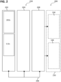
- Fig.2 illustrates the forensics module 250 (also referred to as extraction module) according to various embodiments 200 in a schematic structural diagram, which may, for example, be at least partially integrated into the embedded system 150 according to embodiments 100.
- the forensics module 250 further comprises at least one interface 208 (also referred to as forensics interface 208) configured to communicate with the embedded system 150 (e.g., its components), e.g., with the at least one embedded processor 104 and/or with the memory device 102 of the embedded system 150.
- the communication with the embedded system 150 via the forensics interface 208 may, for example, be privileged to penetrate one or more protection mechanisms of the embedded system 150.
- one or more memory areas of the forensics module may be provided in the memory device 102 of the embedded system 150.
- the functions of the or each forensics processor 204 may be provided by the at least one embedded processor 104 of the embedded system 150, for example, when it executes the forensics code.
- the forensics interface 208 may be provided by hardware and/or software.
- the forensics interface 208 may be provided by a communications protocol.
- the aspects or functions and/or components of the forensics module 250 explained with respect to the integrated forensics module 250 can be provided at least partially (i.e., partially or completely) as a (e.g., physically) standalone component (e.g., its memory area, forensics interface, and/or forensics processor), which can, for example, be retrofitted or added to an existing system architecture.
- the forensics interface 208 can have at least one physical data line, but does not necessarily have to, e.g., if it is implemented via software.
- the at least one forensic processor 204 is configured (e.g., by means of code segments) to forensically extract data (also referred to as state data) representing a system state of the embedded system 150 or CPS by means of the forensic interface 208 (also referred to as extraction for short).
- the state data may represent (e.g., include) the contents (e.g., the data) of one or each register of the at least one processor 104 (e.g., the or each CPU and optionally the or each co-processor) and/or the contents of the or each off-processor data memory 102s, 112s of the embedded system or CPS.
- the state data may represent (e.g., include) the contents of RAM, flash, and CPU, co-processor, and peripheral registers.
- the coordinated approach ensures that no important information for analysis is lost on-site in the absence of the manufacturer. Confidentiality serves to protect the manufacturer's company secrets (e.g., intellectual property (IP)). This protection, in turn, forms the basis of trust for implementing further mechanisms to clarify the incident. Authenticity ensures that the image can be used as evidence for criminal prosecution and to clarify liability issues after the manufacturer has disclosed the image or parts of it (e.g., made it public). Partial disclosure allows the manufacturer to only disclose the To disclose parts of the extracted system state relevant to the attack. It should be noted that larger parts or even the entire system state can also be made available to investigators in order to rule out fraud by the manufacturer in case of doubt.
- IP intellectual property
- the forensic extraction of the system state can be configured to deprive the attacker of the opportunity to compromise the confidentiality, authenticity, and/or availability of the extraction.
- the malicious code e.g., malware
- the CPS state could be manipulated by the malicious code during extraction, for example, to complicate analysis or prevent admissibility in court.
- the malicious code could attempt to prevent the extraction of the system state.
- Fig.3 illustrates the forensic extraction 350 of the system state according to various embodiments 300 in a schematic flow diagram, as it can be or will be implemented, for example, by means of the forensics module 250 (also referred to as extraction module 250) according to the embodiments 200.
- the forensics module 250 also referred to as extraction module 250
- the forensic extraction 350 can be performed within the forensics module 250 and/or the embedded system 150, and optionally started (initiated) from outside the embedded system 150 (e.g., by a so-called extraction trigger).
- the extraction trigger can, for example, be a party or a device, e.g., the investigator or another party.
- the result of the extraction 350 can be output to the extraction trigger in response to the extraction trigger starting the extraction 350.
- Communication between the extraction trigger and the embedded system 150 can take place via a dedicated interface (not shown, also referred to as an extraction interface) of the forensics module 250.
- Forensic extraction 350 can be initiated, for example, by freezing the embedded system 150, e.g., its system state. For this purpose, the embedded system 150 can be stopped.
- the forensic extraction 350 may comprise, in 301, a (e.g., bit-accurate) readout of the state data 302 (e.g., comprising a memory image) by means of the forensics interface 208.
- the reading of the state data 302 of a processor register (e.g., CPU register) and/or peripheral register may be performed by means of a routine dependent on the architecture of the embedded system 150 (also referred to as an architecture-dependent routine), which is implemented, for example, by means of the forensics interface.
- Reading the state data 302 may, for example, involve reading one or more processor registers (e.g., of the CPU, also referred to as CPU registers). Reading each processor register may involve saving a memory image of the or each processor register in the (e.g., secured) memory area of the forensics module 250. This makes it possible to save the context of the running application immediately upon starting the forensic extraction 350. This facilitates the precise extraction of the context of an application, including any potential malware.
- processor registers e.g., of the CPU, also referred to as CPU registers
- Reading each processor register may involve saving a memory image of the or each processor register in the (e.g., secured) memory area of the forensics module 250. This makes it possible to save the context of the running application immediately upon starting the forensic extraction 350. This facilitates the precise extraction of the context of an application, including any potential malware.
- the state data 302 (e.g., a memory image of the embedded system 150) may be cryptographically processed before output (e.g., by the MCU), as explained in more detail below.
- the forensic extraction 350 may include, at 303, determining a commitment 310 (also referred to as a commitment statement) based on the state data 302 and using a cryptographic commitment process 304 (e.g., a vector commitment process). For example, the state data 302 may be mapped to the commitment 310 using the commitment process 304.
- a commitment 310 also referred to as a commitment statement
- a cryptographic commitment process 304 e.g., a vector commitment process.
- An exemplary algorithm also referred to as a commitment algorithm for implementing the commitment process 304 will be described in more detail later.
- the commitment process 304 can be configured such that each data set m k can be verified individually, for example, based on the commitment and/or an opening value d k individually assigned to the data set m k . This ensures that the possibility of partial disclosure exists.
- the forensic extraction 350 may comprise, in 305, encrypting (also referred to as encryption 305) the state data 302 and the opening values d k using a key 305s (e.g., symmetric key 305s).
- the result of the encryption 305 comprises data 312 (also referred to as ciphertext, cryptogram, ciphertext, or ciphertext) comprising the encrypted state data and optionally encrypted opening values d k .
- the key 305s (also referred to as first
- the key 305s or encryption key 305s can be implemented using data (also referred to as key data or key-implementing data) in the secured memory area 202s of the forensics module, as will be explained in more detail later.
- the encryption 305 of the state data and optionally the opening values d k can be performed using an (e.g., symmetric) encryption process 306.
- the encryption process 306 may be an authenticated encryption process 306 that enables the encryption and authentication of the state data using the encryption key 305s unique to the embedded system 150.
- the encryption key 305s may, for example, be known (e.g., only) to the manufacturer.
- the forensic extraction 350 can optionally include, in 307, signing the state data 302.
- the result of the signing 307 comprises the so-called signature 314 of the state data 302.
- the signing 307 can be performed, for example, using a signature process 308 and/or a (e.g., asymmetric) second key 307s (also referred to as a signature key or signing key).
- the signing of the state data 302 enables a unique identification of the state data 302 using the signature key 307s that is unique to the embedded system.
- Encryption 305 can promote the confidentiality of the manufacturer's trade secrets (e.g., IP) as part of the system state vis-à-vis the operator and/or the investigator. Nevertheless, the manufacturer can reveal the system state, for example, after signing a confidentiality agreement.
- the embedded system e.g., CPS
- CPS the embedded system
- the embedded system commits to the content of the state data 302, e.g., the encrypted memory image, at the time of extraction 350 (also referred to as the extraction time). This allows the manufacturer, despite encryption 305, to later prove to the operator and/or the investigator that the revealed system state corresponds to the previously extracted state data 302.
- subsets e.g., one or more than one individual data set m k
- the signature method together with the unique identifier of the state data 302, makes it possible to prove that the state data 302 was created by the embedded system 150 at the time of extraction and not subsequently. (e.g., by the manufacturer).
- the functionality for decrypting, revealing, and verifying the status data 302 is later performed by an emulation system (also referred to as a processing module), which will be described in more detail later.
- the extraction module 250 (e.g., its forensics interface 208) implements a function for the extraction 350 that reads the system state of the EGS 150 (e.g., CPS) and outputs the result of the extraction 350 via a suitable interface, e.g., the networking interface.
- a suitable interface e.g., the networking interface.
- the state data 302 can be encoded in Intel Hex format (also known as IHEX encoding).
- Intel Hex format is particularly simple, offers widespread support, and is easy to read.
- the Intel Hex format also allows the encoding of the state data 302 in the stream, which makes it easier to output the encoded and secured state data 302 directly, in order to minimize memory requirements.
- the state data 302 is available as ASCII strings after IHEX encoding.
- any other suitable encoding can of course also be used, and encoding of the state data 302 is not necessarily required.
- the size of the internal state of extraction 350 is constant in size with the extracted system state. This achieves a lower memory requirement of extraction 350, which will be provided exclusively for extraction 350, and prevents the system state from being extracted only incompletely.
- This is facilitated by two or more components 303, 305, 307 (e.g., comprising: determining 303 the commitment 310, encrypting 305, and/or signing 307) of extraction 350 (e.g., cryptographic processes) running in parallel.
- the system state to be read out e.g., the state data 302
- Fig.4 illustrates the EGS 150 according to various embodiments 400 in a schematic structure diagram (for example, configured according to embodiments 100), which can be transferred in particular to a plurality of embedded systems (or CPS), for example with regard to the implemented security mechanisms.
- CPS embedded systems
- the basis of the forensics module 250 according to embodiments 400 is an STM32L4 MCU as part of the embedded system 150, whose at least one processor 104 comprises a Cortex-M4 CPU.
- the Cortex-M4 CPU has a 32-bit architecture for data and instructions. Registers and buses therefore have a width of 32 bits.
- the Cortex-M4 CPU further has a so-called thumb instruction set or implements a so-called thumb mode. In this thumb mode, a reduced instruction set, the so-called thumb instruction set, is available, in which only 16 bits are required for encoding instructions.
- the Cortex-M4 CPU has two stack pointers: the main stack pointer (MSP) and the process stack pointer (PSP). Which of these stack pointers is accessed by register R13 can be controlled by a bit in the control register (CONTROL).
- the program status register (PSR) contains one or more of the following registers: an application program status register (APSR), an interrupt program status register (IPSR), and/or an execution program status register (EPSR).
- the link register (so-called “link register”, link register or LR for short) is used to store the return address when calling a function.
- the CPU writes the current value of the Program counter ("Program Counter or PC for short) into the link register (LR). This allows you to return from the called function later by setting the program counter to the value stored in the link register (the so-called function return).
- the exception frame for the Cortex-M4 CPU is shown in the following table, which depicts the Cortex-M4 stack frame when the exception occurs.
- the "Address Offset" column indicates the address offset relative to the value of the stack pointer (SP) before the exception occurs.
- the registers R0-R3 and R12 can be overwritten in the exception handler, since they are reconstructed from the stack by the CPU when the handler is exited.
- the exception frame also contains the value of the program counter before the exception was encountered. This allows the CPU to reset the program counter to its state before the exception was encountered at the end of the exception handler.
- the program counter is set to the EXEC_RETURN value that was in the LR when the exception was encountered.
- EXEC_RETURN encodes information about the structure of the exception frame and the mode into which the exception should be exited (handler mode or thread mode). This causes the CPU to exit the exception into the correct mode and restore the exception frame registers.
- one or more security mechanisms are implemented to inhibit or prevent malicious code (e.g., malware) from accessing a secured memory area of the embedded system 150 (e.g., CPS).
- the embedded system 150 e.g., its storage device 102 has a secured memory area 402 (also referred to as trusted memory area 402) and a non-secured memory area 404 (also referred to as untrusted memory area 404).
- the trusted memory area 402 requires higher privileges (also referred to as permissions or authorization levels) to access it than the untrusted memory area 404.
- Hardware-based implementations of the trusted memory area 402 or its isolation from the untrusted memory area 404 include: a memory protection unit (the so-called “Memory Protection Unit” or MPU for short), a trusted runtime environment (the so-called “Trusted Execution Environment” or TEE for short), or a security element (the so-called “Secure Element” or SE for short).
- the MPU is typically controlled by a real-time operating system (RTOS).
- RTOS real-time operating system
- the RTOS implements memory access control and process separation. among each other and between the processes in thread mode and the RTOS in handler mode.
- TEE When using a TEE, all resources of the EGS 150 are separated into a secure and an insecure part. This enables the isolation of security-critical components, for example, from components with access to critical assets such as keys. This separation can also be achieved within the privileged RTOS. This allows security-critical functionalities to be separated from the complex part of the RTOS.
- SE security-critical functionalities are outsourced to a completely separate hardware component, the SE. Examples include a smart card or a trusted platform module (the so-called "Trusted Platform Module,” or TPM for short). This provides a high level of isolation but complicates integration on the application MCU side.
- the trusted memory area 402 it may be important whether it should be accessed only once after system startup, or whether re-entry should occur at runtime, allowing extraction at any time. For runtime access, additional privileges can be granted upon entry. This case places higher demands on the hardware for implementing the trusted memory area 402.
- the impact of re-entry on the functionality of the forensics module 250 is shown in the table below. No re-entry Re-entry Detection Only on reboot, persistent manipulation, boot attestation Anytime, persistent and volatile manipulations, remote attestation in general extraction Only on reboot, persistent state Anytime, overall condition
- a secure re-entry into the trusted memory area 402 places more demands on the hardware than entry via reboot, since the privileges when transitioning from the untrusted to the trusted memory area 402 must be increased upon re-entry.
- each of these exceptions can be configured in such a way that the interrupt cannot be suppressed by the attacker. This can be achieved, for example, by configuring the embedded system 150 in which both the interrupt handler itself and the configuration of the interrupt controller are located within the RoT.
- the specific implementation depends on the type and architecture of the respective embedded system 150 (or CPS), its MCU, and the available access control mechanisms (so-called “access control Mechanisms”). Possible implementation concepts include: an ARM security zone (the so-called "Arm TrustZone"), the firewall, or the MPU.
- the extraction 350 is triggered by an external interrupt (illustratively an interrupt instruction).
- option bytes allow one or more static security mechanisms of the EGS 150 (e.g., microcontroller) to be configured.
- Both flash banks of the EGS 150 e.g., microcontroller
- the option bytes can no longer be changed when RDP Level 2 is enabled, not even by the application on the MCU.
- the firewall is not necessarily part of the static security mechanisms and is therefore not configured or enabled via the option bytes.
- the embedded system 150 e.g., its processor 104, is configured (e.g., as one of the first steps) to verify the configuration of the (e.g., static) security mechanisms (also referred to as a security check).
- the security check may include determining whether the option bytes meet a stored specification (as explained below) and optionally (e.g., if the specification is not met), programming the option bytes (e.g., according to the specification).
- the security check may be provided by a so-called security engine module of the MCU.
- the functions of the security engine described herein may optionally also be provided by the forensics processor 204.
- the embedded system 150 e.g., its processor 104, is configured to continue the boot process (also referred to as system startup) only if it has been determined that the option bytes are configured according to the specification. This reduces the risk that the booted embedded system 150 will be faulty if an attacker succeeds in manipulating the configuration of the option bytes (e.g., through a physical attack).
- the security function unit can also provide the functionality for configuring the dynamic security mechanisms (e.g., firewall).
- RDP Read protection
- RDP is configured to protect the data of the embedded system 150 from external access.
- RDP is configured to protect one or more of the following memory areas from external access: flash memory, option bytes, backup registers, and SRAM2 (SRAM1 is not necessarily protected).
- SRAM2 SRAM1 is not necessarily protected.
- the access rights for the application and the possible accesses via a debug interface are summarized in the table below.
- the RDP option byte can be programmed accordingly, followed by a system reboot. If RDP is set to level 1, it can be reprogrammed, e.g., deactivated. To do this, the option bytes are reprogrammed, e.g., using the debug interface and/or the application. When reprogramming RDP from level 1 to RDP level 0, the entire memory is automatically erased.
- Fig.5 illustrates an exemplary implementation of various security mechanisms of the forensics module 250 according to various embodiments 500 in a schematic structure diagram (for example implemented by means of the embedded system according to embodiments 100 or 400), which can be transferred particularly easily to a plurality of embedded systems (or CPS).
- the debug interface can still be used. In this case, it may be possible to completely reprogram the embedded system 150. Nevertheless, there are use cases where RDP at Level 1 may be suitable even in application-oriented operation, for example, if access to the flash memory is restricted.
- the debug interface in particular, can be used to circumvent the firewall. Therefore, RDP at Level 1 together with the firewall cannot necessarily be reliable, nor can the firewall necessarily meet the security requirements.
- the debug interface can be used to change the boot configuration so that the embedded system 150 boots from SRAM1 or from the ST boot loader. This opens up a potential attack surface when RDP Level 1 is used.
- PCROP is configured to configure one or more memory areas of the non-volatile memory as "executable only” (also referred to as NA memory area). In this case, accesses, such as direct memory access (DMA), debug access, write access, read access, and/or erase access, to this NA memory area are blocked. This area cannot even be addressed via the debug interface, except for execution.
- DMA direct memory access
- debug access write access, read access, and/or erase access
- data also referred to as key-implementing data
- the NA memory area e.g., comprising executable program code (e.g., an assembly function) or other code segments that are configured such that, when executed by the processor, they cause the processor to write the key (e.g., its bytes) directly to an address of another memory area (also referred to as the key target area) of the embedded system 150, which address is specified according to the data.
- executable program code e.g., an assembly function
- other code segments e.g., an assembly function
- the key target area also referred to as the key target area
- the key-implementing data can, of course, also implement the key differently, e.g., if PCROP is not supported or undesired.
- the key-implementing data can be executed from the RoT, which is protected by the firewall, to write the key.
- the key is deleted from the memory, e.g., the key target area, of the embedded system 150.
- the PCROP-protected key ensures that the key is available only as executable code most of the time and is only made available for read access by a cryptographic process when the key is actually needed. This makes an attack on the key more difficult.
- the PCROP_RDP bit can be set to 1 to delete the key in this area. Otherwise, the attacker could set RDP to level 0 and simultaneously disable the protection of the NA memory area using RCROP. In this case, the memory blocks (e.g., flash blocks) containing the key (e.g., as key-implementing data) would not be deleted, and the attacker could read the key.
- the memory blocks e.g., flash blocks
- the entire memory area designated for one or more keys can be secured using PCROP.
- This memory area can, in turn, be located behind the firewall (i.e., in its enclave), specifically in the code region.
- WRP Write protection
- RDP is set to level 2
- WRP can provide a purely internal and, above all, static security measure. For example, option bytes and thus WRP settings cannot be changed. For example, memory areas in the flash can be protected forever from changes using WRP. This makes WRP inflexible as a security mechanism, but can be practical for keys, especially if they should not or must not be changed for the lifetime of the embedded system 150.
- RDP is set to level 1, e.g., in a productive environment, WRP can also be reconfigured, allowing the security mechanism to be temporarily deactivated (e.g., for a firmware update). If a memory area is protected using PCROP secured, an additional WRP hedging mechanism may be redundant.
- a statically secured memory area e.g., of the flash memory
- a dynamically secured memory area can be provided using a firewall (or a dynamic security mechanism).
- the firewall allows the provision of a secured enclave (e.g., comprising one or more memory areas), which, for example, has its own code, its own address range in the flash memory, and/or its own address range in the RAM.
- a secured enclave e.g., comprising one or more memory areas
- Each memory area of the enclave is isolated from the rest of the environment and equipped with very strict access mechanisms, which are provided, for example, by the hardware of the embedded system 150.
- the firewall can, for example, be implemented as a trusted runtime environment. If the firewall is deactivated (e.g., unlike the static security mechanisms) during a system reset (system reboot), it can be activated as part of the initialization process of the embedded system 150. However, the firewall may not yet be activated at system startup, which opens the door to an attack (e.g., a side-channel attack) that could prevent the firewall from being activated and thus circumvent this security mechanism. This can be the case if the embedded system does not have a hardware-based RoT, such as a TPM. In this case, it may be useful to protect the code segments (or instructions) that activate the firewall with WRP (including the interrupt table). Together with RDP at Level 2, this prevents these code segments from being modified, so that the integrity of the forensics module 250 or the TEE can be guaranteed.
- WRP including the interrupt table
- Fig.6 illustrates an exemplary implementation of the firewall 612 of the forensics module 250 according to various embodiments 600 in a schematic layout diagram of the MCU as part of the EGS 150 (e.g., configured according to embodiments 400), which can be transferred in particular to a variety of other embedded systems (or CPS).
- CPS embedded systems
- the embedded system 150 may have at least one firewall-protected memory area 651 (also referred to as FW memory area 651).
- the at least one FW memory area 651 may include one or more than one (e.g., more than two) of the following memory areas: a first flash memory area 602 in which the firmware is stored, a second flash memory area 604 in which data is stored; a RAM memory area 606, which may be exclusive or shared.
- the embedded system 150 may further comprise a DMA controller 608 (also referred to as a DMA control device), which may, for example, be configured to perform memory access (either to the main memory itself or to a peripheral component) independently of the processor 104 (e.g., the Cortex-M4 CPU), e.g., without requiring the processor 104.
- a DMA controller 608 also referred to as a DMA control device
- the processor 104 e.g., the Cortex-M4 CPU
- the at least one FW memory area 651 can be specified using a starting address and the length of each memory area. For example, a granularity of 256 bytes is enforced for the flash memory areas and/or a granularity of 64 bytes for the RAM segment.
- the firewall 612 can be configured to detect (e.g., monitor) all memory accesses to the at least one FW memory area 651 (e.g., to flash and RAM), which occur, for example, via the communication infrastructure 106, e.g., its Advanced High-performance bus (AHB bus), and/or, for each of the memory accesses, to determine whether the memory access is permitted (also referred to as legal), e.g., if it is privileged to do so, or impermissible (also referred to as illegal), e.g., if it is not privileged to do so (also referred to as unprivileged).
- ALB bus Advanced High-performance bus
- the firewall can be configured, for example, to detect where the memory access originates from and, based on this, determine whether this memory access is privileged.
- an authentication sequence which will be described in more detail later, can be privileged to access the FW memory area (also referred to as penetrating the firewall).
- the firewall 612 can, for example, be configured to block unauthorized memory access to the at least one FW memory area 651 (e.g., from outside the protected at least one FW memory area 651) (also referred to as a blocking response).
- the firewall 612 (then also referred to as a closed firewall) can, for example, be configured to reset the embedded system 150 in response to the unauthorized memory access to the at least one FW memory area 651 (also referred to as a reset response).
- the reset response and/or the blocking response can, for example, be implemented using hardware.
- the reset response can, for example, involve the firewall not triggering an interrupt but directly resetting the embedded system 150.
- the firewall 612 can be configured to determine a memory access as permissible (e.g. only) if it is made via an interface configured for this purpose, the so-called Invocation gate (also referred to as call gate).
- the call gate may be configured to increase the privilege level of memory access if it meets a predefined criterion.
- the call gate may be implemented, for example, as a processor function of the forensics processor 204.
- the call gate may be configured to cause a dynamic change in the privilege level of the forensics processor 204 when a specific instruction that meets the criterion is used. In this way, code and programs with fewer privileges can temporarily operate as if they were programs with higher privileges.
- isolated functions can be called in the enclave. This transfers control to the code behind the firewall.
- the call gate can be implemented using a function that receives the input parameters for the enclave behind firewall 612 and returns a response. These input parameters can, for example, address a specific function behind the firewall and return the parameters for this function.
- the call gate can be configured or configured to correspond to firewall 612.
- Fig.7 illustrates a state diagram of a firewall 612 (for example, configured according to embodiments 600) according to various embodiments 700 in a schematic flow diagram, which can in particular be transferred to a plurality of other embedded systems (or CPS).
- a firewall 612 for example, configured according to embodiments 600
- CPS embedded systems
- the code behind the firewall can be executed. Passing through the call gate opens the firewall, allowing it to be penetrated. In this state, the code stored in at least one FW memory area 651 is executed normally, for example, as if there were no firewall at all.
- the firewall can, for example, be configured to either execute the reset response or close the firewall in response to a jump from within the at least one FW memory area 651 to an address outside the at least one FW memory area 651 ("irregular exit from the protected area").
- the firewall can make the decision based on an indication (also referred to as a flag) in a predefined register, which is located in the at least one FW memory area 651 and can be adjusted (for example, Firewall Pre Arm Flag in the register FW_CR). This is an additional safeguard to prevent such jumps. Before the code exits the firewall ("regular exit from the protected area"), this flag is set, and then control is transferred to the application (via a normal return from the function). If this flag is not set and the code leaves the protected area, the firewall interprets this as irregular behavior and resets the embedded system. Interrupts can also be conveniently disabled for this safeguard.
- the firewall can be used to secure one or more algorithms used to implement a cryptographic process and/or one or more cryptographic keys.
- security-critical processes such as a firmware update (also known as a firmware upgrade)
- An algorithm secured in this way is executed in isolation, and only the result is returned. This ensures, for example, that any intermediate results remain securely behind the firewall, which can be important for cryptographic functions. Furthermore, it ensures on a technical level that only dedicated functions can directly access a secured key.
- the firewall is configured to check (e.g., block and/or, if permitted, release) all accesses to the FW memory area 651 (e.g., from the MCU and/or DMA).
- Fig.8 800 illustrates the determination 303 of the commitment 310 (for example, configured according to embodiments 300) by means of a cryptographic vector commitment process (VC process) according to various embodiments 800 in a schematic flowchart.
- the VC process 304 denotes a special commitment process that allows for the individual disclosure of dedicated parts of the extracted system state without violating their authenticity.
- a commitment process allows a party to commit to a piece of information (e.g., status data) without having to disclose the information (also referred to as confidentiality).
- the information therefore remains confidential for the time being.
- the commitment process allows for the possibility of To be able to reveal the information at any given time and ensure that the information remains unchanged (also known as the binding property), e.g., cannot be modified.
- cryptographic measures are used to provide proof (the so-called commitment), which enables the verification of the revealed information.
- a commitment process can have two phases (also called first phase and second phase), each of which can be implemented, for example, using an individual algorithm.
- the commitment 310 can be determined, for example, using a first algorithm (also referred to as a commitment algorithm or commit).
- the commitment algorithm can be configured to output the commitment c and optionally an opening value d as output data based on input data m (e.g., a message or the state data). Expressed as a relation, this can be written as Commit(m) ⁇ (c, d).
- the opening value d is kept secret, and the commitment c is published.
- the opening value d can, for example, be a random number or other random character string, for example, determined using a random generator (also referred to as RAND), and/or can be determined or specified using another mechanism.
- the opening value can be used as a key that parameterizes the commitment process and thus influences the output commitment c (e.g., independently of the input data m).
- the second phase (also called the opening phase), based on the commitment c, it can be determined whether a claim m' (illustratively the claimed input data) corresponds to the original input data m based on the commitment c and the opening value d (also called verification), for example using a second algorithm (also called verification algorithm or ComVrfy).
- the output b can, for example, only take the value 1 or 0.
- a less complex implementation of the commitment process can be achieved by using a cryptographic hash function H as part of the commitment algorithm.
- the random value d is then the opening value and is kept secret.
- the binding property can be enhanced, for example, if the hash function H is collision-resistant, e.g., weakly collision-resistant, preferably strongly collision-resistant, or further preferably perfectly collision-resistant.
- the hash function H can be a collision-resistant one-way function and/or belong to the class of secure hash algorithms.
- the VC process 304 is a special commitment process in which the input data m is multi-component, e.g., having n components. This can be notated, for example, in the easily understandable vector notation, although it should be understood that any other notation for multi-component input data can also be used. Accordingly, the aspects explained with regard to the vector notation can apply analogously to any other notation for multi-component input data.
- the special feature of the VC process 304 is that not necessarily the entire vector m has to be uncovered; rather, individual components m k , with k ⁇ [1, n], can also be uncovered without violating the binding property.
- the commitment algorithm of the VC process can then be written as Commit(m) ⁇ (c, d).
- This partial close algorithm can be used to calculate opening values d I for an index set I ⁇ [n].
- Each aperture value d i can, for example, be determined in advance using a random generator (also called RAND).
- the corresponding verification algorithm can then be written as ComVrfy(c ,d I ,m I ) ⁇ b. This verification algorithm verifies the partially opened data against the commitment c.
- a less complex implementation of the VC process 304 can be achieved using a cryptographic hash function H as part of the commitment algorithm.
- the random values d i together then form the opening value d, which is kept secret.
- the partial close algorithm is designed to reveal a d i for each i ⁇ I, while for the remaining i the c i are computed and revealed as part of d I.
- the final commitment c can be reconstructed or verified from the intermediate commitments c i and the pair (d i , m i ).
- the low-complexity implementation of the VC process 304 using a cryptographic hash function H further ensures that the extraction 350 can be performed in a single pass and with the smallest possible memory requirements.
- the hash function can be instantiated, for example, with SHA-256 from the SHA-2 family (SHA denotes a secure hash algorithm).
- SHA-256 denotes a secure hash algorithm.
- the data is then processed in 64-byte blocks, which corresponds to the internal state of SHA-256.
- SHA-256 it can be understood that what is described herein in this regard can apply analogously to any other SHA.
- the starting point for extraction 350 is a configurable specification of which memory areas of the embedded system 150 are to be read. Logically, this specification can be written as a list of tuples, each of which contains a memory address of the corresponding memory area and the length of the corresponding memory area.
- the memory areas are optionally grouped (also referred to as memory grouping), which is configurable depending on the application. This memory grouping can be relevant for later opening of the data and corresponds to the individual components m k (also referred to as data records) of the input data m for the VC process. This requires that either all memory areas of a group (also referred to as memory group) or no memory areas of the group are revealed. The larger the number n of memory groups, the finer the grid and the more selectively information can be revealed.
- Each section (also called a group section or "section") of a memory group comprises one or more (e.g., contiguous) memory areas, which may, for example, also have a certain logical relationship to each other.
- the register file e.g., of the CPU, for example, forms its own memory group.
- the memory grouping clearly partitions the system state into memory groups, each of which has one or more group sections and/or corresponds to one of the data sets m k .
- a number of n memory groups are formed, each of which has an individual number of l k group sections.
- the k-th memory group for example, has l k group sections, where, for example, l k > 1 and/or l k ⁇ l k+1 can, but need not, be the case.
- the i-th intermediate commitment c i is calculated (e.g., using the hash function), which is processed in the vector commitment state (VC_State). If, for example, SHA-256 is used for this purpose, only an additional 64 bytes are required. Such an instantiation of the VC process requires only 128 bytes. Additionally, a constant overhead can be provided for the concrete implementation of the SHA-256 function.
- an initial vector commitment state is provided (e.g., using a function V_Init) and updated based on the first determined intermediate commitment c 1 (e.g., using a function VC_Update).
- the thus updated vector commitment state can be iteratively updated based on each individual determined intermediate commitment c i .
- the final commitment c is determined based on the last updated vector commitment state and the last determined intermediate commitment c n (e.g., using a function VC_Final).
- Fig.9 illustrates the encryption 305 according to various embodiments 900 in a schematic flow diagram, which may be configured, for example, according to embodiments 300.
- Encryption 305 may, but need not necessarily, run in parallel with determining commitment 310 (e.g., according to embodiments 800). This is particularly useful when both encryption 305 and determining commitment 310 process the same data sets m k or are based on the same storage grouping.
- each individual group section can be encoded in such a way that it is a standalone and valid block (e.g., IHEX block), for example, apart from the missing end-of-file record.
- each block e.g., IHEX block
- IHEX block starts with an extended address so that all information from m i can be uniquely assigned to the respective memory addresses, e.g., without having to see/know other blocks (e.g., IHEX blocks).
- This approach makes it easier to combine the state data into a complete (e.g., IHEX) encoded state when decrypting it later.
- the encryption 305 can be performed using the encryption process 306.
- the encryption process 306 or the encryption 305 can, in an exemplary implementation, use an Authenticated Encryption with Associated Data (AEAD), for example, the so-called Galois/Counter Mode (GCM) with AES (Advanced Encryption Standard) as the block cipher.
- AEAD Authenticated Encryption with Associated Data
- GCM Galois/Counter Mode
- AES Advanced Encryption Standard
- the authenticity can be verified, for example, by the manufacturer, who has access to the device-specific (e.g., symmetric) encryption key 305s.
- a signature can be calculated from the read state data (also referred to as signing 307), as will be explained in more detail later.
- the encryption key 305s may be a system-specific (e.g., symmetric) key, for example, a key uniquely assigned to and/or stored within the embedded system 150. This may be provided by determining the encryption key 305s based on a master key (e.g., of the manufacturer) and the identity of the embedded system 150, for example, using a key derivation function (KDF).
- KDF key derivation function
- An exemplary implementation of the encryption process 306 can be carried out using an (e.g., symmetric) encryption algorithm.
- the encryption algorithm can, for example, be configured to process the state data 302 block by block, whereby the state data 302 can optionally be input byte by byte or even bit by bit. If a complete block is given, it is processed and the result is returned (e.g., using the AEAD_Update function). Similarly and in parallel, the authentication tag (also referred to as "tag”) is calculated, whereby the associated data is initially included in the calculation and no intermediate results need to be output.
- the associated data comprises so-called (e.g., random) moment information (also referred to as "nonce" or one-way information), which is determined at the start of the extraction 350, for example, using a random generator (also referred to as RAND).
- random moment information also referred to as "nonce” or one-way information
- an initial AEAD state (AEAD_State) is provided (e.g., via an AEAD_Init), optionally based on the nonce and/or the encryption key 305s.
- This initial AEAD state is updated based on the first encrypted data set m 1 (e.g., via an AEAD_Update) and subsequently updated with the first encrypted open value d 1 (e.g., via an AEAD_Update).
- the AEAD state updated in this way can be iteratively updated based on each tuple (m i , d i ).
- the final AEAD state (AEAD_Final) is determined based on the last updated AEAD state. Based on the final AEAD state, the cryptogram 312 and/or the tag can be determined.
- the encryption process 306 is configured to require a number of bytes equal to twice the block length (32 bytes in the case of AES).
- a constant overhead which may depend on the exact implementation of the GCM mode, may optionally be provided.
- the memory requirements for the encoding e.g., IHEX encoding
- IHEX encoding the data is encoded in lines of configurable length. For example, 32 bytes can be encoded per line, resulting in 11 + 64 bytes per line.
- a constant overhead can also be provided by the specific implementation of the IHEX encoding.
- the system state or state data is maintained in the memory area of the embedded system 150 reserved for the forensics module 250, which prevents parts of the system state from being overwritten by the embedded system 150.
- Fig.10 illustrates the signing 307 according to various embodiments 1000 in a schematic flow diagram, which can be configured, for example, according to the embodiments 300.
- the signing 307 can run in parallel with the encryption 305 and/or in parallel with the determination 303 of the commitment 312.
- signature 314 can be publicly verified so that it can be used, for example, by investigators and/or in court.
- signing 307 is configured such that signature 314 enables authentication of extracted state data 302, for example, when it is publicly verified, so that the entire state data 302 does not have to be opened.
- signing 307 can be based on encrypted and/or compressed state data 302 (e.g., a cryptogram ct i based thereon).
- An exemplary implementation of the signature process 308 may include first compressing the state data 302 (e.g., using a hash function H) (also referred to as compression), and then determining the signature 314 based on the result of the compression.
- a hash function H also referred to as compression
- an SHA-256 hash function with the 64-byte internal state can be used for compression.
- the specified nonce optionally enters the signature process 308.
- each cryptogram ct i e.g., ciphertext formed using AEAD
- the determined commitment 310 is processed.
- the hash value calculated from it is then signed (e.g., using a "Sign" function). For this purpose, At this point in time, all data has already been processed, so that the internal state for the actual signing 307 does not have to be added to the memory requirement of the extraction 350.
- an initial hash state (HASH_State) is provided (e.g., using a HASH_Init function), optionally based on the nonce.
- the initial hash state is updated based on a first determined cryptogram ct 1 (e.g., using a HASH_Update function), which is based on the first data set m 1 .
- the hash state updated in this way can be iteratively updated based on each determined cryptogram ct i .
- the final hash value h (HashValue) is determined based on the last updated hash state and the commitment 310.
- the signature 314 is determined based on the final hash value h and the signature key 307s.
- a key pair (e.g., consisting of a private signature key 307s and a public key) may be provided for signing 307.
- the public key of the embedded system 150 may, for example, be made available to the investigator.
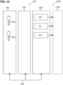
- Fig.11 1100 illustrates the forensics module 250 according to various embodiments in a schematic configuration diagram (e.g., configured according to embodiments 100 and/or 400). As explained above, the encoding, if performed at all, does not necessarily have to be performed using IHEX.
- the forensics module 250 has the trusted storage area 402, which has first key data implementing the encryption key 305s and/or second key data implementing the signature key 307s.
- the first key data and/or second key data can comprise the respectively implemented key as plaintext or an executable program code that causes the processor 104, upon execution of the program code, to write the implemented key to the key target area (e.g., provided in the trusted storage area 402).
- the encryption key 305s (“key”, see Fig.9 ) can be used for authenticated encryption 305.
- the signature key 307s (“sk”, see Fig.10 ) can be used for signing 307.
- the encryption 305 provides confidentiality for the state data 302, which makes it possible to keep parts of the system state or the state data 302, for example trade secrets (e.g. IP) of the manufacturer therein, secret.
- trade secrets e.g. IP
- the opening value of the commitment process is also encrypted to maintain the confidentiality of the commitment process.
- the nonce together with the encrypted state data 302, can be additionally authenticated using AEAD mode. Unlike the signature 314, for example, only the manufacturer can verify the correctness of the tag.
- the signature 314 is calculated, for example, based on the ciphertext 312 and the commitment 310, as well as optionally the nonce.
- the signature 314 is primarily used for integrity verification by a third party, such as a court or investigator.
- the manufacturer does not necessarily have to verify the signature 314 because the nonce is already authenticated by AEAD and because the commitment 310 can be recalculated. This is the reason why the nonce can be used as associated data in AEAD.
- the VC process 304 is a particularly advantageous function of the forensics module 250.
- the VC process 304 enables, for example, protection against a malicious and/or compromised manufacturer.
- the VC process 304 also allows, alternatively or additionally, the publication of only individual parts of the system state or state data 302 (e.g., a single data set), e.g., as needed, e.g., in the event of a legal dispute.
- the VC process 304 also indirectly serves to protect the manufacturer's trade secrets as well as the public interest.
- the investigator can verify whether the state data 302 truly originates from the data packet extracted by him from an embedded system 150 (or investigation case) identified by the nonce, e.g., without having to use the manufacturer's secret keys.
- an embedded system 150 or investigation case identified by the nonce
- By partially opening the system state it is also possible to publish important data pieces, such as malicious code (e.g., malware from the attacker), in court and to cryptographically prove that the state data 302 belongs to the embedded system 150 or the investigation case.
- malicious code e.g., malware from the attacker
- the forensics module 250 further comprises an additional interface 1102 (also referred to as output interface 1102), wherein the at least one processor 104 is configured to send the result of the extraction 350 to a system-external destination 1104 (ie outside the embedded system 150) by means of the output interface 1102. transmit, e.g., to another computing device.
- the result of the extraction 350 may include the commitment 310, the cryptogram 312, and/or the signature 314.
- the target 1104 may, for example, be the extraction trigger and/or be stored by the embedded system 150 (illustratively as a default).
- the output interface 1102 may, for example, be configured as a networking interface, as explained above.
- Extraction 350 which can be initiated during operation, was explained above.
- a similar process for system startup also referred to as boot attestation is explained below.
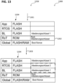
- Fig.12 illustrates a software stack 1250 of the EGS 150 according to various embodiments 1200 in a schematic structural diagram.
- the software stack 1250 represents the system state to be determined and has several layers (also referred to as software layers), of which a lowest (e.g., first) layer provides a secured area 1202 of the RoT (also referred to as RoT layer 1202). Furthermore, the memory area 1204 in which the respective software layers are stored is indicated.
- Each of the software layers can, for example, have parameters (also referred to as program parameters, such as program data) and/or program code.
- the boot attestation described herein allows the reading of the status data 302 to be separated from the attestation (also referred to as authentication).
- the reading of the status data 302 can occur during the system startup of the EGS 150 (or CPS).
- the attestation can then be performed as a protocol between the verifier and the EGS 150 at any later time using an application ("app").
- n 4.
- the i-th data record m i can represent the i-th software layer s i , e.g., comprising its parameters and/or program code (also referred to as code for short).
- the i-th data record can comprise the complete content of the i-th software layer s i .
- Examples of intermediate layers (n>i>0) include: the bootloader ("BL") or the operating system (e.g., an RTOS).
- the RoT layer 1202 includes a so-called root attestation key RK (also referred to as the root attestation key or "root key”), which can be used as the initial attestation key "AK 0 " (also referred to as the reference key AK 0 ).
- the root attestation key can be secured by the firewall and/or PCROP.
- PCROP allows the root attestation key to be protected from internal access in addition to the firewall.
- the system boot of the EGS 150 can occur in stages according to a corresponding sequence (also referred to as the system boot sequence).
- the system boot sequence can comprise several successively executed stages, of which the i-th stage starts or executes exactly the i-th software layer and/or transfers control of the EGS 150 to it.
- the system boot sequence can be implemented by the i-th software layer being configured (e.g., having instructions thereto) to execute the (e.g., immediately) subsequent i+1-th stage of the system boot sequence (e.g., starting the i+1-th software layer).
- the instructions implementing the system boot sequence can also be provided separately from the software stack 1250.
- the EGS 150 (e.g., the forensics processor 204) is configured to perform an attestation sequence (also referred to as an authentication sequence) during the system boot sequence.
- the authentication sequence can be implemented as a separate sequence from the system boot sequence or integrated into the system boot sequence and/or the software stack (e.g., as part of the system boot sequence).
- the i-th software layer is configured to read the (e.g., immediately) subsequent i+1-th software layer and, based thereon, to determine an i+1-th key (also referred to as the i+1-th attestation key). More generally, the i-th software layer can, for example, have instructions to determine the i+1-th attestation key AK i .
- the instructions implementing the attestation sequence can also be provided separately from the software stack 1250.
- the application can perform an attestation with the auditor at any time based on the derived nth attestation key AK n and thereby Verify whether the system state was tampered with during the last system boot.
- the auditor can also initiate a new system boot (e.g., using the extraction trigger) before performing an attestation.
- the software stack 1250 of the EGS 150 can be read during system startup and starting with a secure RoT, for example, with low requirements for each of the software layers s i (i > 0).
- the attestation itself is then performed by the application, for example, without this functionality having to be specially secured (although this may well be the case).
- the cryptographic processing ensures that the attestation can be successfully performed (for example, only) if the system state was not tampered with during system startup.
- the verifier initiates a system startup (also referred to as a boot process)
- the attestation can be successfully completed (for example, only) if the boot process is actually performed.
- the authentication sequence can receive, for example, a nonce N B (also called a boot nonce) as input, which is used as a verification key.
- the boot nonce can be, for example, a number (e.g., a random number) or other random character string that is used only once.
- This boot nonce N B ensures that the auditor can detect if the system restart (also referred to as the reboot process) is suppressed by an attacker.
- a standardized (e.g., saved) nonce can be used as the boot nonce.
- the boot nonce N B can optionally be updated, e.g., set to a new value. Updating the boot nonce can, e.g., be performed by the forensic processor 204 and/or based on information received by the EGS 150 (e.g., specified from outside the system, e.g., by the auditor).
- the root attestation key may be stored in the RoT layer 1202 as a secret key RK (e.g., on a ROM), which is used individually for the EGS 150 (or a series of EGS 150s) and is written during the manufacture of the EGS 150.
- RK secret key
- This root key may be known to the verifier who will perform the attestation.
- the RoT layer 1202 is configured, for example, to instruct or even perform the reading of the (e.g., immediately) subsequent software layer (in this example, BL) by the forensics module 250 (e.g., the forensics processor 204).
- the data set m 1 of the BL can optionally contain sensor data from the EGS 150.
- the first attestation key AK 1 is calculated.
- KDF can, for example, be a cryptographic key derivation function.
- the first attestation key AK 1 is now stored for access by the BL, access to the root key is blocked, and control is transferred to the BL.
- Fig.13 illustrates the state 1350 of the software stack 1250 (software stack) of the system 150 according to various embodiments 1300 in a schematic flow diagram during the attestation sequence, according to which the first attestation key AK 1 was determined and subsequently additional attestation keys are determined.
- the cryptographic process may, for example, be the cryptographic key derivation function.
- the attestation sequence may further comprise, in 1303, determining, before executing the i-th stage of the system startup sequence i ⁇ ⁇ 2, ..., n ⁇ , an i-th attestation key
- AK i (e.g., denoted by Attestation Key 2 or 3) using the cryptographic process based on the data set m i of the i-th level and the (i-1)-th attestation key AK i-1 .
- the i-th attestation key AK i is determined based on the (i-1)-th attestation key AK i-1 instead of the root key, whereupon the (i-1)-th attestation key AK i-1 is securely deleted or overwritten, for example, before being passed to the i-th software layer.
- the BN is no longer necessarily processed for i>2.
- the BN ensures that each boot process is unique and that temporary secrets on various software layers that may have been corrupted are rendered useless.
- This BN is generated, for example, by the extraction trigger (e.g., the verifier) and transmitted to the EGS 150. This ensures that the value of the BN is reset with each extraction.
- the software stack 1250 of the EGS 150 can now be verified (e.g., by the verifier).
- a challenge-response protocol can be implemented between the application and the verifier.
- the verifier selects a random challenge NV (also known as a verifier nonce or PN) and sends it to the EGS 150 as a knowledge request.
- NV also known as a verifier nonce or PN
- the application answers this challenge by issuing a proof of knowledge (also called proof-of-knowledge) for the attestation key, e.g. in the form of a message authentication code (also called MAC), for example according to the relation r ⁇ MAC(AK n , NV).
- a proof of knowledge also called proof-of-knowledge
- MAC message authentication code
- the application can transmit both the boot nonce and the results h 1 , ..., h n to the tester. This can be useful if multiple valid software versions of the EGS 150 exist and the tester needs to quickly identify the current version.
- these results h 1 , ..., h n do not necessarily have to be separately secured against tampering, since the verifier can only use the results h 1 , ..., h n for the assignment, whereas the system state is guaranteed by the cryptographically secured response r to the challenge. Knowing the response r, the verifier can now perform the same calculations that were performed during the boot process, based on its copy of the root key RK, the boot nonce NB and the expected device state (m' 1 , ... ,m' n ) or (h' 1 , ...
- the output b can only take the value 1 or 0.
- the attestation sequence is executed on the selected microcontroller.
- a firewall is used to protect the root key.
- the firewall is configured and switched on and set up in such a way that any attempt to access the memory area of the root key is immediately answered by the embedded system 150 being reset by the firewall (e.g., by means of a hardware reset by the firewall), e.g., by executing the reset response. If the functionality of the firewall is fully implemented, e.g., to place code segments that implement the extraction 350 behind the firewall or in the enclave, the root key can still be placed behind the firewall.
- the root key can be additionally secured by means of a PCROP, which could protect against unintentional access when using the firewall in this way.
- the RoT layer e.g., containing the root key
- the RoT layer can be stored in the ROM of the EGS 150 and/or secured by the firewall.
- the option bytes can be used as additional data.
- the input data of the attestation sequence is used to derive the attestation key.
- AK n Once the very last attestation key AK n has been generated, it can be verified.
- a challenge is generated for the EGS 150.
- the previously generated boot nonce can be sent to the EGS 150.
- the EGS 150 receives the instruction to restart the software along with the boot nonce (in practice, this can be done differently).
- the boot nonce is used to determine the attestation key AK n , and after the restart is complete, the application reports, for example, with the new boot nonce.
- the actual attestation is performed after the restart.
- the new challenge is sent to the EGS 150.
- the EGS 150 can only answer the challenge correctly if a reboot with the specified boot nonce was performed beforehand and the actual system state of the EGS 150 (also referred to as the actual system state) corresponds to the expected system state (also referred to as the target system state).
- the emulation system is discussed in more detail below.
- Fig.14 illustrates an emulation system 1450 according to various embodiments 1400 in a schematic configuration diagram.
- the emulation system 1450 is configured to emulate the EGS 150 system, which includes the embedded processor 104 and the at least one sensor 110 and/or at least one actuator 112.
- the emulation system 1450 has a digital interface 1410 for receiving the (e.g., decrypted) state data 302, a (physical) communication interface 1408 (also referred to as peripheral interface) to at least one sensor 1408s (also referred to as emulation sensor 1408s) and/or at least one actuator 1408a (also referred to as emulation actuator).
- the or each emulation sensor can be identical to the respective sensor 110 of the EGS 150 or at least an emulated representation thereof.
- the or each emulation actuator 1408a can be identical to the respective actuator 112 of the EGS 150 or at least an emulated representation thereof.
- one or more than one sensor 110 and/or one or more than one actuator of the EGS 150 can be emulated as emulation actuator 1408a or emulation sensor 1408s, respectively.
- the emulation actuator can represent a motor of the EGS 150 (e.g., be identical to it or at least an emulated representation thereof).
- the emulation processor 1404 is further configured to communicate via the communication interface 1408 in the same way as the embedded processor 104 communicates via the functional interface 108, e.g., with the at least one sensor 110 or at least one actuator 112 of the EGS 150.
- the emulation system 1450 further comprises a storage device 1402 (e.g., comprising one or more than one data memory 102s, 112s).
- a storage device 1402 e.g., comprising one or more than one data memory 102s, 112s.
- the emulation system 1450 further comprises a communication infrastructure 1406 (e.g., comprising a CAN bus or other field bus) which couples at least the memory device 1402, the emulation processor 1404, the digital interface 1410, and/or the communication interface 1408 to one another.
- a communication infrastructure 1406 e.g., comprising a CAN bus or other field bus
- the emulation system 1450 may be configured to reconstruct the system state based on the state data 302 (also referred to as reconstruction or restoration), e.g., in handler mode.
- Reconstruction may, for example, include reconstructing the processor register (e.g., CPU register) and/or peripheral register.
- Reconstruction in handler mode provides extended privileges that are beneficial for the execution of certain instructions and can occur, for example, if the CPU registers were also saved in handler mode. To continue the code at this point after reconstruction, the CPU can be in the same mode. This ensures that reconstruction with the appropriate code to exit handler mode is executed correctly.
- the corresponding exception to enter handler mode can be triggered (e.g., instructed) by writing the interrupt control and state register (ICSR), either by software from thread mode or by the debugger.
- ISR interrupt control and state register
- the forensics module 250 can install the corresponding interrupt handler.
- Writing the ICSR triggers a non-maskable interrupt (NMI).
- NMI non-maskable interrupt
- the flash memory can be or become partitioned in such a way that the functionality for reconstructing the processor register (e.g., CPU core register) as part of the forensics module 250 is located in a flash memory area that does not necessarily have to be physically present in the MCU of the EGS 150. This way, programming the memory image does not overwrite the forensics module 250.
- the processor register e.g., CPU core register
- the RAM can contain the following data, which can be automatically reconstructed by loading the RAM background: stack, heap, register file (e.g., CPU register file).
- the RAM can be written directly by a debugger, for example.
- the emulation system 1450 can be configured in such a way that, after reconstructing the RAM and peripheral registers, the code for reconstructing the processor register (e.g., CPU register) is executed immediately.
- Writing the ICSR can trigger an NMI, thus placing the CPU in handler mode. This jumps to the NMI exception handler that the forensics module 250 has installed accordingly. This makes it easier for the CPU to continue in handler mode after reconstruction if the memory dump was executed within an interrupt handler.
- the RAM contents can then be reconstructed using a restore command.
- the peripheral registers are mapped into the MCU's address space. Like flash memory and RAM, they can initially be mapped from the extracted state into a separate file. An exception to this is the status registers, which in some cases cannot always be written via the software interface; their contents can only be modified by manipulating the hardware. For example, the input register of an IO pin reflects the state of the pin and can often only be modified by applying a corresponding potential to the pin itself. A peripheral emulator can be used to reconstruct the state of such registers.
- processor registers cannot necessarily be written directly. In this case, they are written using dedicated processor instructions (e.g., CPU instructions).
- the exception handler can be exited and the system state can be set to the correct program code address. This can be done, for example, by loading an exception return or return address. This causes the CPU to exit handler mode and load the exception frame from the stack.
- An exemplary emulation system 1450 is configured to emulate relevant components of the EGS 150, including, for example, the memory device 102, the embedded processor 104, the communication infrastructure 106, and/or the interface 108. For example, at least the embedded processor 104 and the interface 108 may be emulated.
- the emulation MCU can be controlled from the analysis PC via a debug adapter. This allows for step-by-step execution of the program code, setting breakpoints, memory analysis, and more.
- An exemplary implementation of the emulation system 1450 for a generic EGS 150 may include, for example, an STM32L476 Nucleo development board with an STM32L4 MCU.
- An exemplary implementation of the emulation system 1450 for a manufacturer-specific EGS 150 may include, for example, a manufacturer-specific development board with a Cortex M4 MCU and
- peripheral emulator peripheral emulator.
- component Generic emulation Payout Emulation CPU Core Arm Cortex-M4 Arm Cortex-M4 Debug interface SWD JTAG Debug Probe ST-LINK V2 Green Hills Sample Debugger Gnu Debugger (GDB) Green Hills TimeMachine Debugger Peripheral Emulator Rigol DG4162 function generator FPGA and Rigol DG4162
- the emulation system 1450 may be configured to perform an automatic analysis of the result of the extraction 350. This is explained below.
- Fig.15 illustrates an analysis system 1550 according to various embodiments 1500 in a schematic structural diagram and a detailed view 1501, which comprises the emulation system 1450 according to the embodiments 1400 (e.g., a CPS emulation system, CPS emulation for short).
- the emulation system 1450 e.g., a CPS emulation system, CPS emulation for short.
- the emulation system 1450 can be provided, for example, via an emulation board.
- the emulation system 1450 emulates, for example, the MCU of the EGS 150 (or CPS) and its peripherals (e.g., having one or more sensors and/or actuators).
- the emulation system 1450 is used to execute the malicious code to be analyzed, if present, and offers extended functionalities, such as one or more debug interfaces and peripheral components.
- the system PC of the analysis system 1550 (more commonly referred to as the environment emulation device) emulates the system PC of the attacked device (e.g., an ATM) that has the EGS 150 or CPS. Beyond the functionality of a "normal" system PC, the system PC of the 1550 analysis system is configured to run additional analysis software.
- the analysis PC is configured to control the remaining components of the analysis system 1550.
- the required software for incident analysis is executed on the analysis PC and the result of the extraction 350 (e.g., the status data 302) is saved.
- the USB analyzer (also referred to as USB analysis device) is configured to analyze the USB communication between the components of the analysis system 1550, for example, the system PC and the emulation system 1450.
- the USB analyzer may, for example, be configured to record, manipulate, and/or play one or more messages of the USB communication.
- the CAN bus analyzer is configured to analyze CAN bus communication (or more generally, communication via the communication infrastructure 1406 of the emulation system 1450).
- the analyzer offers the ability to record, manipulate, and/or externally import one or more messages transmitted via the communication infrastructure 1406.
- the function generator is configured for synchronous emulation of sensor signals.
- the analysis PC is configured to use the function generator to specifically input a signal synchronously with the CPS program flow.
- the optional oscilloscope is set up to analyze peripheral and bus signals and to synchronously control the function generator.
- An (optionally controllable) laboratory power supply (not shown) is configured to supply power to the 1450 emulation system. If the laboratory power supply is controllable, a power failure or other power-related attack can be emulated by controlling the laboratory power supply (e.g., using the analysis PC).
- the debug probe implements the debug protocols of the EGS 150 MCU (for example, a so-called Joint Test Action Group (JTAG) or Single Wire Debug (SWD)) and connects the MCU of the 1450 emulation system to the analysis PC.
- JTAG Joint Test Action Group
- SWD Single Wire Debug
- An exemplary implementation shows the instantiation of the USB analyzer using "ellisys USB Explorer 200", the instantiation of the oscilloscope using "Lecroy
- WaveRunner 640Zi the instantiation of the function generator using "Rigol DG4162”
- the debug interface of the 1450 emulation system can be used for reconstruction. This allows programming of FLASH memory and writing to and reading from RAM and registers.
- the peripheral registers are memory-addressable. Processor registers, for example, can only be accessed indirectly via special instructions.
Landscapes
- Engineering & Computer Science (AREA)
- Theoretical Computer Science (AREA)
- Computer Security & Cryptography (AREA)
- Software Systems (AREA)
- Computer Hardware Design (AREA)
- General Engineering & Computer Science (AREA)
- Physics & Mathematics (AREA)
- General Physics & Mathematics (AREA)
- General Health & Medical Sciences (AREA)
- Bioethics (AREA)
- Health & Medical Sciences (AREA)
- Business, Economics & Management (AREA)
- Storage Device Security (AREA)
- Accounting & Taxation (AREA)
- Finance (AREA)
- Debugging And Monitoring (AREA)
- Development Economics (AREA)
- Economics (AREA)
- Strategic Management (AREA)
- General Business, Economics & Management (AREA)
Claims (20)
- Module d'informatique légale (250) pour un système intégré (150), le module d'informatique légale (250) présentant :• une zone de mémoire sécurisée (202s) qui présente de premières données qui mettent en œuvre une clé (305s) ;• une interface (208) pour lire (301) de deuxièmes données (302) représentant un état de système du système intégré (150) ; et• un ou plusieurs processeurs (204),qui est conçu pour :• lire (301) les deuxièmes données (302) au moyen de l'interface (208), les deuxièmes données (302) présentant plusieurs jeux de données ;• déterminer (303) un engagement (310) concernant plusieurs valeurs d'ouverture dont chaque valeur d'ouverture est associée à exactement l'un des plusieurs jeux de données, sur la base des deuxièmes données (302) et en utilisant un processus d'engagement cryptographique qui est conçu de telle sorte que chaque jeu de données peut être vérifié individuellement à l'aide de l'engagement (310) et de la valeur d'ouverture respectivement associée ;• crypter (305) les deuxièmes données (302) et les plusieurs valeurs d'ouverture en utilisant la clé (305s).
- Module d'informatique légale (250) selon la revendication 1, dans lequel le processus d'engagement met en œuvre une fonction de hachage cryptographique, de préférence résistante aux collisions, qui permet de déterminer l'engagement (310).
- Module d'informatique légale (250) selon la revendication 1 ou 2, dans lequel le processus d'engagement est un processus d'engagement vectoriel.
- Module d'informatique légale (250) selon l'une quelconque des revendications 1 à 3, dans lequel l'engagement (310) est lié aux plusieurs valeurs d'ouverture et/ou aux deuxièmes données (302).
- Module d'informatique légale (250) selon l'une quelconque des revendications 1 à 4, présentant en outre :• une interface supplémentaire (208),• dans lequel ledit un ou les plusieurs processeurs (204) sont en outre conçus pour sortir les deuxièmes données cryptées (302) et l'engagement (310) au moyen de l'interface supplémentaire (208).
- Module d'informatique légale (250) selon l'une quelconque des revendications 1 à 5, dans lequel le cryptage est effectué en utilisant la clé (305s) au moyen d'un processus de cryptage symétrique.
- Module d'informatique légale (250) selon l'une quelconque des revendications 1 à 6, dans lequel le cryptage est effectué en utilisant la clé (305s) au moyen d'un processus de cryptage authentifié.
- Module d'informatique légale (250) selon l'une quelconque des revendications 1 à 7, dans lequel le cryptage en utilisant la clé (305s) présente le cryptage de plusieurs jeux de données par itération.
- Module d'informatique légale (250) selon l'une quelconque des revendications 1 à 8, dans lequel la zone de mémoire est sécurisée au moyen d'un ou de plusieurs des éléments suivants :• d'un pare-feu ;• d'une unité de protection de mémoire ;• d'une protection en écriture ; et/ou• d'une protection en lecture.
- Module d'informatique légale (250) selon l'une quelconque des revendications 1 à 9, dans lequel la détermination (303) de l'engagement (310) présente la détermination des plusieurs valeurs d'ouverture, de préférence au moyen d'un générateur de valeurs aléatoires.
- Module d'informatique légale (250) selon l'une quelconque des revendications 1 à 10, dans lequel l'interface (208) est conçue pour lire un registre de processeur du système intégré (150), dans lequel de préférence la lecture (301) des deuxièmes données (302) est effectuée au moyen de l'interface (208) à partir du registre de processeur.
- Module d'informatique légale (250) selon la revendication 11, dans lequel les deuxièmes données (302) présentent une image du registre de processeur du système intégré (150).
- Module d'informatique légale (250) selon l'une quelconque des revendications 1 à 12, dans lequel la détermination (303) de l'engagement et le cryptage (305) des deuxièmes données sont effectués en même temps.
- Module d'informatique légale (250) selon l'une quelconque des revendications 1 à 13, dans lequel l'interface (208) est en outre conçue pour arrêter le système intégré (150), de préférence son processeur (204), et les deuxièmes données (302) sont lues par le système intégré arrêté (150).
- Système intégré (150), présentant :• le module d'informatique légale (250) selon l'une quelconque des revendications 1 à 14 ; et• une ou plusieurs zones de mémoire supplémentaires (102s, 112s), dans lequel l'interface (208) est conçue pour lire les deuxièmes données (302) à partir de ladite une ou des plusieurs zones de mémoire supplémentaires (102s, 112s) ;• dans lequel de préférence ladite une ou les plusieurs zones de mémoire supplémentaires (102s, 112s) présentent un registre de processeur.
- Système intégré (150) selon la revendication 15, présentant en outre :• un actionneur (112) et/ou un capteur (110) ; et• de préférence un firmware pour piloter le capteur et/ou l'actionneur, le firmware étant mémorisé dans ladite une ou les plusieurs zones de mémoire supplémentaires (102s, 112s).
- Distributeur automatique présentant le système intégré (150) selon la revendication 15 ou 16.
- Distributeur automatique selon la revendication 17, dans lequel le système intégré (150) est conçu pour remplir une fonction du distributeur automatique• en relation avec un dépôt, une présentation et/ou un retrait d'un document de valeur, et/ou• en relation avec une authentification d'une personne.
- Procédé pour un système intégré (150), le procédé présentant les étapes consistant à :• lire (301) des données (302) qui représentent un état de système du système intégré (150) au moyen d'une interface (208) qui est conçue pour lire les données, les données (302) présentant plusieurs jeux de données ;• déterminer (303) un engagement (310) concernant plusieurs valeurs d'ouverture dont chaque valeur d'ouverture est associée à exactement l'un des plusieurs jeux de données, sur la base des données (302) et en utilisant un processus d'engagement cryptographique qui est conçu de telle sorte que chaque jeu de données peut être vérifié individuellement à l'aide de l'engagement et de la valeur d'ouverture respectivement associée ;• crypter (305) les données (302) et les plusieurs valeurs d'ouverture en utilisant une clé (305s) qui est mise en œuvre au moyen de données supplémentaires qui sont mémorisées dans une zone de mémoire sécurisée (202s).
- Support de stockage non volatile, présentant des segments de code qui sont conçus, lorsqu'ils sont exécutés par un processeur (104, 204), pour faire que le processeur (104, 204) exécute le procédé selon la revendication 19.
Applications Claiming Priority (2)
| Application Number | Priority Date | Filing Date | Title |
|---|---|---|---|
| DE102021110768.7A DE102021110768B3 (de) | 2021-04-27 | 2021-04-27 | Forensik-Modul und eingebettetes System |
| PCT/EP2022/060832 WO2022229060A1 (fr) | 2021-04-27 | 2022-04-25 | Module médico-légal et système intégré |
Publications (2)
| Publication Number | Publication Date |
|---|---|
| EP4330842A1 EP4330842A1 (fr) | 2024-03-06 |
| EP4330842B1 true EP4330842B1 (fr) | 2025-05-28 |
Family
ID=81846503
Family Applications (1)
| Application Number | Title | Priority Date | Filing Date |
|---|---|---|---|
| EP22725414.1A Active EP4330842B1 (fr) | 2021-04-27 | 2022-04-25 | Module médico-légal et système intégré |
Country Status (4)
| Country | Link |
|---|---|
| US (1) | US20240193564A1 (fr) |
| EP (1) | EP4330842B1 (fr) |
| DE (1) | DE102021110768B3 (fr) |
| WO (1) | WO2022229060A1 (fr) |
Family Cites Families (29)
| Publication number | Priority date | Publication date | Assignee | Title |
|---|---|---|---|---|
| GB9715684D0 (en) * | 1997-07-25 | 1997-10-01 | Computer Forensics Limited | Integrity verification and authentication of copies of computer data |
| WO2007117261A2 (fr) * | 2005-07-26 | 2007-10-18 | Digimarc Corporation | fonctionnalité médico-légale pour des documents sécurisés |
| EP1958147A1 (fr) * | 2005-11-24 | 2008-08-20 | Koninklijke Philips Electronics N.V. | Filigrane d expertise multibit avec clé de détection codée |
| JPWO2008117556A1 (ja) * | 2007-03-28 | 2010-07-15 | 日本電気株式会社 | ログ取得システム、ログ収集端末、ログ取得端末、それらを用いたログ取得方法及びプログラム |
| US8331775B2 (en) * | 2009-10-15 | 2012-12-11 | Jack Harper | Fingerprint scanning systems and methods |
| US8391481B2 (en) * | 2009-12-31 | 2013-03-05 | International Business Machines Corporation | Rebinding of content title keys in clusters of devices with distinct security levels |
| US10057298B2 (en) * | 2011-02-10 | 2018-08-21 | Architecture Technology Corporation | Configurable investigative tool |
| US9904788B2 (en) * | 2012-08-08 | 2018-02-27 | Amazon Technologies, Inc. | Redundant key management |
| US11017069B2 (en) * | 2013-03-13 | 2021-05-25 | Lookout, Inc. | Method for changing mobile communications device functionality based upon receipt of a second code and the location of a key device |
| US20150304289A1 (en) * | 2014-04-22 | 2015-10-22 | Electronics And Telecommunications Research Institute | Notarization agent and method for collecting digital evidence using notarization agent |
| US9565200B2 (en) * | 2014-09-12 | 2017-02-07 | Quick Vault, Inc. | Method and system for forensic data tracking |
| US10079686B2 (en) * | 2015-07-29 | 2018-09-18 | International Business Machines Corporation | Privacy-preserving attribute-based credentials |
| US10079842B1 (en) | 2016-03-30 | 2018-09-18 | Amazon Technologies, Inc. | Transparent volume based intrusion detection |
| EP3769466B1 (fr) * | 2018-03-23 | 2025-06-18 | nChain Licensing AG | Système et procédé mis en oeuvre par ordinateur pour permettre une preuve de connaissance nulle |
| EP3565179B1 (fr) * | 2018-04-30 | 2022-10-19 | Merck Patent GmbH | Marquage de sécurité composite et procédés et appareils pour le fournir et le lire |
| EP3793129B1 (fr) * | 2018-05-30 | 2025-04-23 | Huawei International Pte. Ltd. | Système, procédé et appareil d'échange de clé |
| MX2019004360A (es) * | 2018-11-27 | 2019-08-05 | Alibaba Group Holding Ltd | Sistema y metodo para proteccion de la informacion. |
| US11586728B2 (en) * | 2019-06-07 | 2023-02-21 | Nxp B.V. | Methods for detecting system-level trojans and an integrated circuit device with system-level trojan detection |
| US11601443B2 (en) | 2019-09-25 | 2023-03-07 | Acronis International Gmbh | System and method for generating and storing forensics-specific metadata |
| US11223487B2 (en) * | 2020-03-19 | 2022-01-11 | Jinan University | Method and system for secure blockchain-based vehicular digital forensics |
| US20220076253A1 (en) * | 2020-09-06 | 2022-03-10 | David Chaum | Computation mixing |
| US11586738B2 (en) * | 2020-12-03 | 2023-02-21 | Dell Products, L.P. | Systems and methods for evaluating security risks using a manufacturer-signed software identification manifest |
| US11522708B2 (en) * | 2020-12-18 | 2022-12-06 | Dell Products, L.P. | Trusted local orchestration of workspaces |
| US20220239502A1 (en) * | 2021-01-27 | 2022-07-28 | Anderson Software LLC | System to Securely Issue and Count Electronic Ballots |
| DE102021110766B3 (de) * | 2021-04-27 | 2022-06-23 | Wincor Nixdorf International Gmbh | Forensik-Modul und eingebettetes System |
| US12204642B2 (en) * | 2021-11-17 | 2025-01-21 | Dell Products, L.P. | Hardware-based protection of application programming interface (API) keys |
| CN114338006B (zh) * | 2021-12-24 | 2023-01-24 | 浙江大学 | 基于半可信硬件的互相关伪随机数的远程获取方法及装置 |
| US12086252B2 (en) * | 2022-02-18 | 2024-09-10 | Saudi Arabian Oil Company | System and method for preserving forensic computer data |
| WO2023233419A1 (fr) * | 2022-06-04 | 2023-12-07 | Sanjeev Dr | Scène de véhicule de crime basée sur l'iot avec système de gestion de preuve médico-légale intégré (fems) |
-
2021
- 2021-04-27 DE DE102021110768.7A patent/DE102021110768B3/de active Active
-
2022
- 2022-04-25 US US18/287,812 patent/US20240193564A1/en active Pending
- 2022-04-25 EP EP22725414.1A patent/EP4330842B1/fr active Active
- 2022-04-25 WO PCT/EP2022/060832 patent/WO2022229060A1/fr not_active Ceased
Also Published As
| Publication number | Publication date |
|---|---|
| EP4330842A1 (fr) | 2024-03-06 |
| WO2022229060A1 (fr) | 2022-11-03 |
| DE102021110768B3 (de) | 2022-06-23 |
| US20240193564A1 (en) | 2024-06-13 |
Similar Documents
| Publication | Publication Date | Title |
|---|---|---|
| DE102021110766B3 (de) | Forensik-Modul und eingebettetes System | |
| EP2899714B1 (fr) | Préparation sécurisée d'une clé | |
| DE112009002502B4 (de) | Multilayer inhalte-schützender Mikrocontoller | |
| EP2742643B1 (fr) | Dispositif et procédé de décryptage de données | |
| DE60129967T2 (de) | Auf biometrie basierende beglaubigung in einer nichtflüchtigen speichervorrichtung | |
| DE102004062203B4 (de) | Datenverarbeitungseinrichtung, Telekommunikations-Endgerät und Verfahren zur Datenverarbeitung mittels einer Datenverarbeitungseinrichtung | |
| DE102009013384B4 (de) | System und Verfahren zur Bereitstellung einer sicheren Anwendungsfragmentierungsumgebung | |
| DE102013114953B4 (de) | System-on-Chip mit eingebettetem Sicherheitsmodul | |
| DE102008006759A1 (de) | Prozessor-Anordnungen, Prozessor, Verfahren zum Betreiben einer Prozessor-Anordnung | |
| DE102014208855A1 (de) | Verfahren zum Durchführen einer Kommunikation zwischen Steuergeräten | |
| DE10200288A1 (de) | Eine Vorrichtung zur Ausführung von Anwendungen, die sichere Transaktionen und/oder Zugangskontrolle zu werthaltigen Inhalten und/oder Dienstleistungen umfassen, und Verfahren zum Schutz einer solchen Vorrichtung | |
| WO2011054639A1 (fr) | Module matériel cryptographique et procédé d'actualisation d'une clé cryptographique | |
| EP3577873B1 (fr) | Unité de sécurité en particulier pour un appareil iot et procédé d'exécution d'une ou plusieurs applications d'échange de données sécurisé avec un ou plusieurs serveurs de fournisseur de service web | |
| DE102016210788B4 (de) | Komponente zur Verarbeitung eines schützenswerten Datums und Verfahren zur Umsetzung einer Sicherheitsfunktion zum Schutz eines schützenswerten Datums in einer solchen Komponente | |
| DE102020216030A1 (de) | Verfahren zum abgesicherten Start einer Recheneinheit | |
| EP4330842B1 (fr) | Module médico-légal et système intégré | |
| EP3720039A1 (fr) | Procédé de configuration d'un module de sécurité au moyen d'au moins une clé dérivée | |
| EP3248136B1 (fr) | Procédé de fonctionnement d'une unité d'ordinateur avec un environnement de temps d'exécution sécurisé et unité d'ordinateur | |
| DE102014208848A1 (de) | Verfahren zum Überwachen eines elektronischen Sicherheitsmoduls | |
| WO2022229153A1 (fr) | Système d'émulation et procédé | |
| EP3819804A1 (fr) | Vérification de l'intégrité d'un contenu de registre | |
| DE102014208840A1 (de) | Verfahren zum Behandeln von Software-Funktionen in einem Steuergerät | |
| DE102022202688A1 (de) | Verfahren zur Validierung von Daten in einer Recheneinheit | |
| DE102014208844A1 (de) | Verfahren zum Durchführen von sicherheitskritischen Vorgängen in einem Steuergerät | |
| DE102014209037B4 (de) | Vorrichtung und Verfahren zum Schutz der Integrität von Betriebssysteminstanzen |
Legal Events
| Date | Code | Title | Description |
|---|---|---|---|
| STAA | Information on the status of an ep patent application or granted ep patent |
Free format text: STATUS: UNKNOWN |
|
| STAA | Information on the status of an ep patent application or granted ep patent |
Free format text: STATUS: THE INTERNATIONAL PUBLICATION HAS BEEN MADE |
|
| PUAI | Public reference made under article 153(3) epc to a published international application that has entered the european phase |
Free format text: ORIGINAL CODE: 0009012 |
|
| STAA | Information on the status of an ep patent application or granted ep patent |
Free format text: STATUS: REQUEST FOR EXAMINATION WAS MADE |
|
| 17P | Request for examination filed |
Effective date: 20231023 |
|
| AK | Designated contracting states |
Kind code of ref document: A1 Designated state(s): AL AT BE BG CH CY CZ DE DK EE ES FI FR GB GR HR HU IE IS IT LI LT LU LV MC MK MT NL NO PL PT RO RS SE SI SK SM TR |
|
| DAV | Request for validation of the european patent (deleted) | ||
| DAX | Request for extension of the european patent (deleted) | ||
| GRAP | Despatch of communication of intention to grant a patent |
Free format text: ORIGINAL CODE: EPIDOSNIGR1 |
|
| STAA | Information on the status of an ep patent application or granted ep patent |
Free format text: STATUS: GRANT OF PATENT IS INTENDED |
|
| INTG | Intention to grant announced |
Effective date: 20241118 |
|
| GRAS | Grant fee paid |
Free format text: ORIGINAL CODE: EPIDOSNIGR3 |
|
| GRAA | (expected) grant |
Free format text: ORIGINAL CODE: 0009210 |
|
| STAA | Information on the status of an ep patent application or granted ep patent |
Free format text: STATUS: THE PATENT HAS BEEN GRANTED |
|
| AK | Designated contracting states |
Kind code of ref document: B1 Designated state(s): AL AT BE BG CH CY CZ DE DK EE ES FI FR GB GR HR HU IE IS IT LI LT LU LV MC MK MT NL NO PL PT RO RS SE SI SK SM TR |
|
| REG | Reference to a national code |
Ref country code: GB Ref legal event code: FG4D Free format text: NOT ENGLISH |
|
| REG | Reference to a national code |
Ref country code: CH Ref legal event code: EP |
|
| REG | Reference to a national code |
Ref country code: IE Ref legal event code: FG4D Free format text: LANGUAGE OF EP DOCUMENT: GERMAN Ref country code: DE Ref legal event code: R096 Ref document number: 502022004081 Country of ref document: DE |
|
| REG | Reference to a national code |
Ref country code: NL Ref legal event code: MP Effective date: 20250528 |
|
| PG25 | Lapsed in a contracting state [announced via postgrant information from national office to epo] |
Ref country code: FI Free format text: LAPSE BECAUSE OF FAILURE TO SUBMIT A TRANSLATION OF THE DESCRIPTION OR TO PAY THE FEE WITHIN THE PRESCRIBED TIME-LIMIT Effective date: 20250528 Ref country code: ES Free format text: LAPSE BECAUSE OF FAILURE TO SUBMIT A TRANSLATION OF THE DESCRIPTION OR TO PAY THE FEE WITHIN THE PRESCRIBED TIME-LIMIT Effective date: 20250528 |
|
| REG | Reference to a national code |
Ref country code: LT Ref legal event code: MG9D |
|
| PG25 | Lapsed in a contracting state [announced via postgrant information from national office to epo] |
Ref country code: GR Free format text: LAPSE BECAUSE OF FAILURE TO SUBMIT A TRANSLATION OF THE DESCRIPTION OR TO PAY THE FEE WITHIN THE PRESCRIBED TIME-LIMIT Effective date: 20250829 Ref country code: NO Free format text: LAPSE BECAUSE OF FAILURE TO SUBMIT A TRANSLATION OF THE DESCRIPTION OR TO PAY THE FEE WITHIN THE PRESCRIBED TIME-LIMIT Effective date: 20250828 |
|
| PG25 | Lapsed in a contracting state [announced via postgrant information from national office to epo] |
Ref country code: PL Free format text: LAPSE BECAUSE OF FAILURE TO SUBMIT A TRANSLATION OF THE DESCRIPTION OR TO PAY THE FEE WITHIN THE PRESCRIBED TIME-LIMIT Effective date: 20250528 Ref country code: NL Free format text: LAPSE BECAUSE OF FAILURE TO SUBMIT A TRANSLATION OF THE DESCRIPTION OR TO PAY THE FEE WITHIN THE PRESCRIBED TIME-LIMIT Effective date: 20250528 |
|
| PG25 | Lapsed in a contracting state [announced via postgrant information from national office to epo] |
Ref country code: BG Free format text: LAPSE BECAUSE OF FAILURE TO SUBMIT A TRANSLATION OF THE DESCRIPTION OR TO PAY THE FEE WITHIN THE PRESCRIBED TIME-LIMIT Effective date: 20250528 |
|
| PG25 | Lapsed in a contracting state [announced via postgrant information from national office to epo] |
Ref country code: HR Free format text: LAPSE BECAUSE OF FAILURE TO SUBMIT A TRANSLATION OF THE DESCRIPTION OR TO PAY THE FEE WITHIN THE PRESCRIBED TIME-LIMIT Effective date: 20250528 |
|
| PG25 | Lapsed in a contracting state [announced via postgrant information from national office to epo] |
Ref country code: RS Free format text: LAPSE BECAUSE OF FAILURE TO SUBMIT A TRANSLATION OF THE DESCRIPTION OR TO PAY THE FEE WITHIN THE PRESCRIBED TIME-LIMIT Effective date: 20250828 |
|
| PG25 | Lapsed in a contracting state [announced via postgrant information from national office to epo] |
Ref country code: IS Free format text: LAPSE BECAUSE OF FAILURE TO SUBMIT A TRANSLATION OF THE DESCRIPTION OR TO PAY THE FEE WITHIN THE PRESCRIBED TIME-LIMIT Effective date: 20250928 |
|
| PG25 | Lapsed in a contracting state [announced via postgrant information from national office to epo] |
Ref country code: LV Free format text: LAPSE BECAUSE OF FAILURE TO SUBMIT A TRANSLATION OF THE DESCRIPTION OR TO PAY THE FEE WITHIN THE PRESCRIBED TIME-LIMIT Effective date: 20250528 |
|
| PG25 | Lapsed in a contracting state [announced via postgrant information from national office to epo] |
Ref country code: DK Free format text: LAPSE BECAUSE OF FAILURE TO SUBMIT A TRANSLATION OF THE DESCRIPTION OR TO PAY THE FEE WITHIN THE PRESCRIBED TIME-LIMIT Effective date: 20250528 Ref country code: SM Free format text: LAPSE BECAUSE OF FAILURE TO SUBMIT A TRANSLATION OF THE DESCRIPTION OR TO PAY THE FEE WITHIN THE PRESCRIBED TIME-LIMIT Effective date: 20250528 |
|
| PG25 | Lapsed in a contracting state [announced via postgrant information from national office to epo] |
Ref country code: CZ Free format text: LAPSE BECAUSE OF FAILURE TO SUBMIT A TRANSLATION OF THE DESCRIPTION OR TO PAY THE FEE WITHIN THE PRESCRIBED TIME-LIMIT Effective date: 20250528 |
|
| PG25 | Lapsed in a contracting state [announced via postgrant information from national office to epo] |
Ref country code: EE Free format text: LAPSE BECAUSE OF FAILURE TO SUBMIT A TRANSLATION OF THE DESCRIPTION OR TO PAY THE FEE WITHIN THE PRESCRIBED TIME-LIMIT Effective date: 20250528 |
|
| PG25 | Lapsed in a contracting state [announced via postgrant information from national office to epo] |
Ref country code: SK Free format text: LAPSE BECAUSE OF FAILURE TO SUBMIT A TRANSLATION OF THE DESCRIPTION OR TO PAY THE FEE WITHIN THE PRESCRIBED TIME-LIMIT Effective date: 20250528 |
|
| PG25 | Lapsed in a contracting state [announced via postgrant information from national office to epo] |
Ref country code: IT Free format text: LAPSE BECAUSE OF FAILURE TO SUBMIT A TRANSLATION OF THE DESCRIPTION OR TO PAY THE FEE WITHIN THE PRESCRIBED TIME-LIMIT Effective date: 20250528 |
|
| REG | Reference to a national code |
Ref country code: DE Ref legal event code: R097 Ref document number: 502022004081 Country of ref document: DE |
|
| PLBE | No opposition filed within time limit |
Free format text: ORIGINAL CODE: 0009261 |
|
| STAA | Information on the status of an ep patent application or granted ep patent |
Free format text: STATUS: NO OPPOSITION FILED WITHIN TIME LIMIT |
|
| PGFP | Annual fee paid to national office [announced via postgrant information from national office to epo] |
Ref country code: GB Payment date: 20260319 Year of fee payment: 5 |
|
| REG | Reference to a national code |
Ref country code: CH Ref legal event code: L10 Free format text: ST27 STATUS EVENT CODE: U-0-0-L10-L00 (AS PROVIDED BY THE NATIONAL OFFICE) Effective date: 20260409 |
|
| PGFP | Annual fee paid to national office [announced via postgrant information from national office to epo] |
Ref country code: FR Payment date: 20260320 Year of fee payment: 5 |