EP4331840A1 - Dünnschichtelement, transparentes fälschungssicheres element und datenträger - Google Patents
Dünnschichtelement, transparentes fälschungssicheres element und datenträger Download PDFInfo
- Publication number
- EP4331840A1 EP4331840A1 EP22794225.7A EP22794225A EP4331840A1 EP 4331840 A1 EP4331840 A1 EP 4331840A1 EP 22794225 A EP22794225 A EP 22794225A EP 4331840 A1 EP4331840 A1 EP 4331840A1
- Authority
- EP
- European Patent Office
- Prior art keywords
- thin film
- refractive
- film element
- index dielectric
- dielectric layers
- Prior art date
- Legal status (The legal status is an assumption and is not a legal conclusion. Google has not performed a legal analysis and makes no representation as to the accuracy of the status listed.)
- Granted
Links
Images


Classifications
-
- B—PERFORMING OPERATIONS; TRANSPORTING
- B32—LAYERED PRODUCTS
- B32B—LAYERED PRODUCTS, i.e. PRODUCTS BUILT-UP OF STRATA OF FLAT OR NON-FLAT, e.g. CELLULAR OR HONEYCOMB, FORM
- B32B27/00—Layered products comprising a layer of synthetic resin
- B32B27/36—Layered products comprising a layer of synthetic resin comprising polyesters
-
- B—PERFORMING OPERATIONS; TRANSPORTING
- B32—LAYERED PRODUCTS
- B32B—LAYERED PRODUCTS, i.e. PRODUCTS BUILT-UP OF STRATA OF FLAT OR NON-FLAT, e.g. CELLULAR OR HONEYCOMB, FORM
- B32B33/00—Layered products characterised by particular properties or particular surface features, e.g. particular surface coatings; Layered products designed for particular purposes not covered by another single class
-
- B—PERFORMING OPERATIONS; TRANSPORTING
- B32—LAYERED PRODUCTS
- B32B—LAYERED PRODUCTS, i.e. PRODUCTS BUILT-UP OF STRATA OF FLAT OR NON-FLAT, e.g. CELLULAR OR HONEYCOMB, FORM
- B32B7/00—Layered products characterised by the relation between layers; Layered products characterised by the relative orientation of features between layers, or by the relative values of a measurable parameter between layers, i.e. products comprising layers having different physical, chemical or physicochemical properties; Layered products characterised by the interconnection of layers
- B32B7/02—Physical, chemical or physicochemical properties
- B32B7/023—Optical properties
-
- B—PERFORMING OPERATIONS; TRANSPORTING
- B32—LAYERED PRODUCTS
- B32B—LAYERED PRODUCTS, i.e. PRODUCTS BUILT-UP OF STRATA OF FLAT OR NON-FLAT, e.g. CELLULAR OR HONEYCOMB, FORM
- B32B9/00—Layered products comprising a layer of a particular substance not covered by groups B32B11/00 - B32B29/00
-
- B—PERFORMING OPERATIONS; TRANSPORTING
- B32—LAYERED PRODUCTS
- B32B—LAYERED PRODUCTS, i.e. PRODUCTS BUILT-UP OF STRATA OF FLAT OR NON-FLAT, e.g. CELLULAR OR HONEYCOMB, FORM
- B32B9/00—Layered products comprising a layer of a particular substance not covered by groups B32B11/00 - B32B29/00
- B32B9/04—Layered products comprising a layer of a particular substance not covered by groups B32B11/00 - B32B29/00 comprising such particular substance as the main or only constituent of a layer, which is next to another layer of the same or of a different material
- B32B9/045—Layered products comprising a layer of a particular substance not covered by groups B32B11/00 - B32B29/00 comprising such particular substance as the main or only constituent of a layer, which is next to another layer of the same or of a different material of synthetic resin
-
- B—PERFORMING OPERATIONS; TRANSPORTING
- B42—BOOKBINDING; ALBUMS; FILES; SPECIAL PRINTED MATTER
- B42D—BOOKS; BOOK COVERS; LOOSE LEAVES; PRINTED MATTER CHARACTERISED BY IDENTIFICATION OR SECURITY FEATURES; PRINTED MATTER OF SPECIAL FORMAT OR STYLE NOT OTHERWISE PROVIDED FOR; DEVICES FOR USE THEREWITH AND NOT OTHERWISE PROVIDED FOR; MOVABLE-STRIP WRITING OR READING APPARATUS
- B42D25/00—Information-bearing cards or sheet-like structures characterised by identification or security features; Manufacture thereof
- B42D25/20—Information-bearing cards or sheet-like structures characterised by identification or security features; Manufacture thereof characterised by a particular use or purpose
-
- B—PERFORMING OPERATIONS; TRANSPORTING
- B42—BOOKBINDING; ALBUMS; FILES; SPECIAL PRINTED MATTER
- B42D—BOOKS; BOOK COVERS; LOOSE LEAVES; PRINTED MATTER CHARACTERISED BY IDENTIFICATION OR SECURITY FEATURES; PRINTED MATTER OF SPECIAL FORMAT OR STYLE NOT OTHERWISE PROVIDED FOR; DEVICES FOR USE THEREWITH AND NOT OTHERWISE PROVIDED FOR; MOVABLE-STRIP WRITING OR READING APPARATUS
- B42D25/00—Information-bearing cards or sheet-like structures characterised by identification or security features; Manufacture thereof
- B42D25/20—Information-bearing cards or sheet-like structures characterised by identification or security features; Manufacture thereof characterised by a particular use or purpose
- B42D25/23—Identity cards
-
- B—PERFORMING OPERATIONS; TRANSPORTING
- B42—BOOKBINDING; ALBUMS; FILES; SPECIAL PRINTED MATTER
- B42D—BOOKS; BOOK COVERS; LOOSE LEAVES; PRINTED MATTER CHARACTERISED BY IDENTIFICATION OR SECURITY FEATURES; PRINTED MATTER OF SPECIAL FORMAT OR STYLE NOT OTHERWISE PROVIDED FOR; DEVICES FOR USE THEREWITH AND NOT OTHERWISE PROVIDED FOR; MOVABLE-STRIP WRITING OR READING APPARATUS
- B42D25/00—Information-bearing cards or sheet-like structures characterised by identification or security features; Manufacture thereof
- B42D25/20—Information-bearing cards or sheet-like structures characterised by identification or security features; Manufacture thereof characterised by a particular use or purpose
- B42D25/24—Passports
-
- B—PERFORMING OPERATIONS; TRANSPORTING
- B42—BOOKBINDING; ALBUMS; FILES; SPECIAL PRINTED MATTER
- B42D—BOOKS; BOOK COVERS; LOOSE LEAVES; PRINTED MATTER CHARACTERISED BY IDENTIFICATION OR SECURITY FEATURES; PRINTED MATTER OF SPECIAL FORMAT OR STYLE NOT OTHERWISE PROVIDED FOR; DEVICES FOR USE THEREWITH AND NOT OTHERWISE PROVIDED FOR; MOVABLE-STRIP WRITING OR READING APPARATUS
- B42D25/00—Information-bearing cards or sheet-like structures characterised by identification or security features; Manufacture thereof
- B42D25/30—Identification or security features, e.g. for preventing forgery
-
- B—PERFORMING OPERATIONS; TRANSPORTING
- B42—BOOKBINDING; ALBUMS; FILES; SPECIAL PRINTED MATTER
- B42D—BOOKS; BOOK COVERS; LOOSE LEAVES; PRINTED MATTER CHARACTERISED BY IDENTIFICATION OR SECURITY FEATURES; PRINTED MATTER OF SPECIAL FORMAT OR STYLE NOT OTHERWISE PROVIDED FOR; DEVICES FOR USE THEREWITH AND NOT OTHERWISE PROVIDED FOR; MOVABLE-STRIP WRITING OR READING APPARATUS
- B42D25/00—Information-bearing cards or sheet-like structures characterised by identification or security features; Manufacture thereof
- B42D25/30—Identification or security features, e.g. for preventing forgery
- B42D25/324—Reliefs
-
- B—PERFORMING OPERATIONS; TRANSPORTING
- B42—BOOKBINDING; ALBUMS; FILES; SPECIAL PRINTED MATTER
- B42D—BOOKS; BOOK COVERS; LOOSE LEAVES; PRINTED MATTER CHARACTERISED BY IDENTIFICATION OR SECURITY FEATURES; PRINTED MATTER OF SPECIAL FORMAT OR STYLE NOT OTHERWISE PROVIDED FOR; DEVICES FOR USE THEREWITH AND NOT OTHERWISE PROVIDED FOR; MOVABLE-STRIP WRITING OR READING APPARATUS
- B42D25/00—Information-bearing cards or sheet-like structures characterised by identification or security features; Manufacture thereof
- B42D25/30—Identification or security features, e.g. for preventing forgery
- B42D25/328—Diffraction gratings; Holograms
-
- B—PERFORMING OPERATIONS; TRANSPORTING
- B42—BOOKBINDING; ALBUMS; FILES; SPECIAL PRINTED MATTER
- B42D—BOOKS; BOOK COVERS; LOOSE LEAVES; PRINTED MATTER CHARACTERISED BY IDENTIFICATION OR SECURITY FEATURES; PRINTED MATTER OF SPECIAL FORMAT OR STYLE NOT OTHERWISE PROVIDED FOR; DEVICES FOR USE THEREWITH AND NOT OTHERWISE PROVIDED FOR; MOVABLE-STRIP WRITING OR READING APPARATUS
- B42D25/00—Information-bearing cards or sheet-like structures characterised by identification or security features; Manufacture thereof
- B42D25/30—Identification or security features, e.g. for preventing forgery
- B42D25/36—Identification or security features, e.g. for preventing forgery comprising special materials
-
- B—PERFORMING OPERATIONS; TRANSPORTING
- B42—BOOKBINDING; ALBUMS; FILES; SPECIAL PRINTED MATTER
- B42D—BOOKS; BOOK COVERS; LOOSE LEAVES; PRINTED MATTER CHARACTERISED BY IDENTIFICATION OR SECURITY FEATURES; PRINTED MATTER OF SPECIAL FORMAT OR STYLE NOT OTHERWISE PROVIDED FOR; DEVICES FOR USE THEREWITH AND NOT OTHERWISE PROVIDED FOR; MOVABLE-STRIP WRITING OR READING APPARATUS
- B42D25/00—Information-bearing cards or sheet-like structures characterised by identification or security features; Manufacture thereof
- B42D25/30—Identification or security features, e.g. for preventing forgery
- B42D25/36—Identification or security features, e.g. for preventing forgery comprising special materials
- B42D25/373—Metallic materials
-
- C—CHEMISTRY; METALLURGY
- C23—COATING METALLIC MATERIAL; COATING MATERIAL WITH METALLIC MATERIAL; CHEMICAL SURFACE TREATMENT; DIFFUSION TREATMENT OF METALLIC MATERIAL; COATING BY VACUUM EVAPORATION, BY SPUTTERING, BY ION IMPLANTATION OR BY CHEMICAL VAPOUR DEPOSITION, IN GENERAL; INHIBITING CORROSION OF METALLIC MATERIAL OR INCRUSTATION IN GENERAL
- C23C—COATING METALLIC MATERIAL; COATING MATERIAL WITH METALLIC MATERIAL; SURFACE TREATMENT OF METALLIC MATERIAL BY DIFFUSION INTO THE SURFACE, BY CHEMICAL CONVERSION OR SUBSTITUTION; COATING BY VACUUM EVAPORATION, BY SPUTTERING, BY ION IMPLANTATION OR BY CHEMICAL VAPOUR DEPOSITION, IN GENERAL
- C23C14/00—Coating by vacuum evaporation, by sputtering or by ion implantation of the coating forming material
- C23C14/22—Coating by vacuum evaporation, by sputtering or by ion implantation of the coating forming material characterised by the process of coating
- C23C14/24—Vacuum evaporation
- C23C14/26—Vacuum evaporation by resistance or inductive heating of the source
-
- C—CHEMISTRY; METALLURGY
- C23—COATING METALLIC MATERIAL; COATING MATERIAL WITH METALLIC MATERIAL; CHEMICAL SURFACE TREATMENT; DIFFUSION TREATMENT OF METALLIC MATERIAL; COATING BY VACUUM EVAPORATION, BY SPUTTERING, BY ION IMPLANTATION OR BY CHEMICAL VAPOUR DEPOSITION, IN GENERAL; INHIBITING CORROSION OF METALLIC MATERIAL OR INCRUSTATION IN GENERAL
- C23C—COATING METALLIC MATERIAL; COATING MATERIAL WITH METALLIC MATERIAL; SURFACE TREATMENT OF METALLIC MATERIAL BY DIFFUSION INTO THE SURFACE, BY CHEMICAL CONVERSION OR SUBSTITUTION; COATING BY VACUUM EVAPORATION, BY SPUTTERING, BY ION IMPLANTATION OR BY CHEMICAL VAPOUR DEPOSITION, IN GENERAL
- C23C14/00—Coating by vacuum evaporation, by sputtering or by ion implantation of the coating forming material
- C23C14/22—Coating by vacuum evaporation, by sputtering or by ion implantation of the coating forming material characterised by the process of coating
- C23C14/24—Vacuum evaporation
- C23C14/28—Vacuum evaporation by wave energy or particle radiation
- C23C14/30—Vacuum evaporation by wave energy or particle radiation by electron bombardment
-
- C—CHEMISTRY; METALLURGY
- C23—COATING METALLIC MATERIAL; COATING MATERIAL WITH METALLIC MATERIAL; CHEMICAL SURFACE TREATMENT; DIFFUSION TREATMENT OF METALLIC MATERIAL; COATING BY VACUUM EVAPORATION, BY SPUTTERING, BY ION IMPLANTATION OR BY CHEMICAL VAPOUR DEPOSITION, IN GENERAL; INHIBITING CORROSION OF METALLIC MATERIAL OR INCRUSTATION IN GENERAL
- C23C—COATING METALLIC MATERIAL; COATING MATERIAL WITH METALLIC MATERIAL; SURFACE TREATMENT OF METALLIC MATERIAL BY DIFFUSION INTO THE SURFACE, BY CHEMICAL CONVERSION OR SUBSTITUTION; COATING BY VACUUM EVAPORATION, BY SPUTTERING, BY ION IMPLANTATION OR BY CHEMICAL VAPOUR DEPOSITION, IN GENERAL
- C23C14/00—Coating by vacuum evaporation, by sputtering or by ion implantation of the coating forming material
- C23C14/22—Coating by vacuum evaporation, by sputtering or by ion implantation of the coating forming material characterised by the process of coating
- C23C14/34—Sputtering
-
- G—PHYSICS
- G09—EDUCATION; CRYPTOGRAPHY; DISPLAY; ADVERTISING; SEALS
- G09F—DISPLAYING; ADVERTISING; SIGNS; LABELS OR NAME-PLATES; SEALS
- G09F3/00—Labels, tag tickets, or similar identification or indication means; Seals; Postage or like stamps
- G09F3/02—Forms or constructions
Definitions
- the present invention is a National Stage Filing of the PCT International Application No: PCT/CN2022/074032 filed on 26 January, 2022 , which claims priority to and the benefit of Chinese Patent Application No. 202110449714.0, filed to the China National Intellectual Property Administration (CHIPA) on 25 April 2021 , which is hereby incorporated by reference in its entirety.
- CHIPA China National Intellectual Property Administration
- the present invention relates to the technical field of anti-counterfeiting, and in particular to a thin film element, a transparent anti-counterfeiting element, and a data carrier.
- data carriers such as banknotes and financial instruments (for example, value or supporting documents) and other valuable items (for example, luxury brand items) are often equipped with security elements to verify the authenticity of the data carriers and prevent them from being reproduced without authority.
- security elements for example, value or supporting documents
- other valuable items for example, luxury brand items
- the objective of the present invention is to provide a thin film element.
- the thin film element is more practical and more difficult to reproduce.
- the thin film element includes at least two low-refractive-index dielectric layers, at least two high-refractive-index dielectric layers, and at least one translucent reflective layer, the at least two high-refractive-index dielectric layers are located between the at least two low-refractive-index dielectric layers, the at least one translucent reflective layer is located between the two high-refractive-index dielectric layers, the thin film element presents at least two colors after reflection on one surface and reflection and transmission on the other surface.
- a refractive index of the at least two high-refractive-index dielectric layers is at least 0.3 higher than a refractive index of the at least two low-refractive-index dielectric layers.
- a refractive index of the at least two low-refractive-index dielectric layers ranges from 1.2 to 1.7.
- a refractive index of the at least two high-refractive-index dielectric layers ranges from 1.7 to 2.5.
- a thickness of each of the at least two high-refractive-index dielectric layers ranges from 50nm to 300nm.
- one of structures of the thin film element is: the low-refractive-index dielectric layer, the high-refractive-index dielectric layer, the translucent reflective layer, the high-refractive-index dielectric layer, and the low-refractive-index dielectric layer in sequence.
- a thickness of the at least one translucent reflective layer is not greater than 30nm.
- the at least one translucent reflective layer is a metal layer.
- a material of the metal layer is one of Al, Ag, Cu, Cr, Ni, Fe and Au.
- the at least one translucent reflective layer is provided with a hollowed-out area.
- the at least one translucent reflective layer is made of semi-metal.
- the at least one translucent reflective layer is made of silicon or germanium.
- a color difference between the at least two colors in a CIELab color space is not less than 40.
- the thin film element presents a form of a pattern, text or a code.
- each layer structure of the thin film element is provided with a relief structure.
- the relief structure is one or a combination of a micro-optical relief structure, a diffraction relief structure, and a sub-wavelength relief structure.
- Some other embodiments of the present invention further provide a transparent anti-counterfeiting element.
- the transparent anti-counterfeiting element includes a carrier and the thin film element above mentioned arranged on the carrier.
- Still some other embodiments of the present invention further provide a data carrier.
- the data carrier is provided with the thin film element above mentioned.
- the thin film element is disposed in a transparent window area, or in a through hole, or above the through hole of the data carrier.
- the data carrier is a value document, a banknote, or an identity card.
- the thin film element according to the present invention includes the at least two low-refractive-index dielectric layers, the at least two high-refractive-index dielectric layers, and the at least one translucent reflective layer, the at least two high-refractive-index dielectric layers are located between the at least two low-refractive-index dielectric layers, the at least one translucent reflective layer is located between the two high-refractive-index dielectric layers, and the thin film element presents the at least two colors after reflection on one surface and reflection and transmission on the other surface.
- the thin film element is able to be used as an anti-counterfeiting element, so as to achieve being more practical and more difficult to reproduce.
- Transparent windows have proven to be attractive anti-counterfeiting elements in polymer banknotes and, more recently, in paper banknotes as well because a plurality of security features are allowed.
- the special role of authenticity protection is played by an anti-counterfeiting element with view-based effects, as these effects are not able to be reproduced even with the most modern photocopiers.
- the anti-counterfeiting element here is provided with an optically variable element which conveys different image impressions to a viewer from different viewing angles, for example, displaying different color impressions or brightness impressions and/or different graphic patterns depending on the viewing angle.
- a transparent anti-counterfeiting element that shows an appearance contrast between an overhead view and a transmitted light view.
- Fig. 1 is a schematic structural diagram of a thin film element according to an embodiment of the present invention.
- the thin film element includes at least two low-refractive-index dielectric layers 11 (for example, a layer L1 and a layer L2), at least two high-refractive-index dielectric layers 12 (for example, a layer H1 and a layer H2), and at least one translucent reflective layer 13 (for example, a layer M).
- the at least two high-refractive-index dielectric layers 12 are located between the at least two low-refractive-index dielectric layers 11.
- the at least one translucent reflective layer 13 is located between the two high-refractive-index dielectric layers 12.
- the thin film element presents at least two colors after reflection on one surface and reflection and transmission on the other surface.
- a refractive index of the at least two high-refractive-index dielectric layers 12 is at least 0.3 higher than a refractive index of the at least two low-refractive-index dielectric layers 11.
- the refractive index of the at least two low-refractive-index dielectric layers 11 ranges from 1.2 to 1.7.
- the refractive indexes of the layer L1 and the layer L2 are about 1.5.
- the refractive index of the at least two high-refractive-index dielectric layers 12 ranges from 1.7 to 2.5.
- the refractive indexes of the layer H1 and the layer H2 are about 2.2.
- one of structures of the thin film element is: the low-refractive-index dielectric layer 11, the high-refractive-index dielectric layer 12, the translucent reflective layer 13, the high-refractive-index dielectric layer 12, and the low-refractive-index dielectric layer 11 in sequence.
- the thin film element is of a symmetrical five-layer structure L1/H1/M/H2/L2.
- the at least one translucent reflective layer 13 is a metal layer.
- a material of the metal layer is one of Al, Ag, Cu, Cr, Ni, Fe and Au.
- the translucent reflective layer 13 is made of metal, and depending on a thickness, the translucent reflective layer 13 is a homogeneous continuous film layer, or is formed by clusters, that is, by films with discontinuities. An optical effect of Fabry-Perot resonance also occurs in this case.
- a thickness of the at least one translucent reflective layer 13 is not greater than 30nm.
- the thin film element is of the symmetrical five-layer structure L1/H1/M/H2/L2, wherein L1 and L2 are the low-refractive-index dielectric layers 11, H1 and H2 are the high-refractive-index dielectric layers 12, and the absorptivity of visible light by dielectric materials is very low.
- the refractive indexes of L1 and L2 are about 1.5, wherein L1 is a plastic substrate, L2 is a polymer protective layer, and thicknesses of the two are greater than 1 ⁇ m, preferably, greater than 3 ⁇ m.
- the refractive indexes of H1 and H2 are greater than 1.7, and H1 has the same thickness as H2.
- M is a metal Ag or Al layer with a thickness of 15nm.
- the thin film element is of an asymmetrical five-layer structure, wherein L1 and L2 are the low-refractive-index dielectric layers 11, H1 and H2 are the high-refractive-index dielectric layers 12, and the absorptivity of visible light by dielectric materials is very low.
- the refractive indexes of L1 and L2 are about 1.5, where L1 is a plastic substrate, L2 is a polymer protective layer, and thicknesses of the two are greater than 1 ⁇ m, preferably, greater than 3 ⁇ m.
- H1 and H2 have different materials and/or thicknesses, and the refractive indexes of the two are greater than 1.7.
- M is a metal Ag or Al layer with a thickness of 15nm.
- the above thin film structure is a PET/ZnS/AI/ZnS/ polymer coating system.
- a thickness of each of the at least two high-refractive-index dielectric layers 12 ranges from 50nm to 300nm.
- the high-refractive-index dielectric layers 12 are made of ZnS or TiO 2 .
- the layer thickness of the high-refractive-index dielectric layers 12 is generally between 50nm and 300nm. As the color impression of the thin film element is essentially determined by the layer thickness of the high-refractive-index dielectric layers 12, as described in detail below, the thickness is selected based on a desired color impression intensity.
- L1 is a low-refractive-index transparent substrate
- H1 is a high-refractive-index dielectric
- M is a metal layer
- H2 is a high-refractive-index dielectric
- L2 is a low-refractive-index coating.
- the refractive indexes of the layer L1 and the layer L2 are 1.2-1.7, preferably 1.4-1.5.
- the refractive indexes of the layer H1 and the layer H2 are selected as 1.7-2.5, and the thicknesses are 50-300 nm, preferably, 100-200nm.
- the layer M is a metal or semi-metal layer, with the thickness being not greater than 30nm, and is able to simultaneously partially reflect and partially transmit incident light.
- the incident light 21 is incident from an upper surface of the thin film element and produces reflected light and transmitted light. The observer will see the reflected light on the same side of the incident light, and the observer will see the transmitted light on the opposite side of the incident light. In the thin film element, the reflected light is different from the transmitted light in color.
- a color difference between the at least two colors in a CIELab color space is not less than 40.
- the thin film element presents bright metal luster and is essentially achromatic when viewed in the reflected light, and is colorful when viewed in the transmitted light.
- the chroma C ab ⁇ of the thin film element in the transmitted light is greater than 15, preferably, greater than 20, and particularly preferably, greater than 25.
- the chroma C ab ⁇ is specified in the CIELab color space.
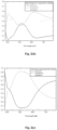
- Table 2-Reflection color and transmission color of an exemplary thin film element 2 PET/ZnS/AI/ZnS/PET laminated thickness (nm) Reflection color Transmission color 15000/120/12/120/15000 Golden Blue 15000/140/8/140/15000 Magenta Cyan 15000/180/8/180/15000 Cyan Tangerine 15000/200/8/200/15000 Green Magenta 15000/220/8/220/15000 Golden Blue
- L1 is PET
- H1 is ZnS
- M is Ag
- H2 is ZnS
- L2 is PET
- L1 is PET
- H1 is ZnS
- M is Al
- H2 is ZnS
- L2 is PET
- the thin film element is colored in the transmitted light and has a color-shift effect.
- the color impression of the thin film element changes in the transmitted light, for example, changing from magenta in a vertical view to green in a tilted view.
- the thin film element is colored in the transmitted light, and when the thin film element is tilted, the thin film element does not change color substantially, but has a transparent color with a change in chroma C ab ⁇
- the color impression in the transmitted light is, for example, blue, and the chroma of the blue transparent color changes from a high value in the vertical view to a low value in the tilted view. In this case, when the thin film element is tilted, only the saturation of the recognizable blue transparent color changes.
- each layer structure of the thin film element is provided with a relief structure.
- the relief structure is one or a combination of a micro-optical relief structure, a diffraction relief structure, and a sub-wavelength relief structure.
- the at least one surface of the layers of the thin film element according to the embodiment of the present invention is provided with the relief structure, such as a diffraction relief structure (for example, a hologram), a micro-optical relief structure (for example, three-dimensional reproduction of a microlens structure and a serrated structure), or a sub-wavelength grating, moth-eye structure.
- the thin film element according to the embodiment of the present invention is also able to be combined with an optically variable coating, in particular with a coating that has a combination of a color variable area and a color constant area.
- Fig. 3 is a schematic structural diagram of the thin film element with the relief structure according to an embodiment of the present invention.
- the structure of the thin film element is, from top to bottom: the low-refractive-index dielectric layer 11 is a low-refractive-index transparent substrate, the high-refractive-index dielectric layer 12 is a high-refractive-index dielectric, the translucent reflective layer 13 is a metal layer, the high-refractive-index dielectric layer 12 is the high-refractive-index dielectric, and the low-refractive-index dielectric layer 11 is a low-refractive-index coating.
- the refractive index of the low-refractive-index dielectric layers 11 is 1.2-1.7, preferably 1.4-1.
- the refractive index of the high-refractive-index dielectric layers 12 is selected as 1.7-2.5, and the thickness is 50-300nm, preferably, 100-200nm.
- the translucent reflective layer 13 is a metal or semi-metal layer, with the thickness being not greater than 30nm, and is able to simultaneously partially reflect and partially transmit incident light.
- the at least one surface of the low-refractive-index dielectric layers 11, the high-refractive-index dielectric layers 12, and the translucent reflective layer 13 is modulated by a surface relief structure 20.
- the surface relief structure 20 is a diffraction relief structure (for example, a hologram), a micro-optical relief structure (for example, three-dimensional reproduction of a microlens structure and a serrated structure), or a sub-wavelength grating, moth-eye structure.
- a transverse size of the diffraction relief structure is 0.7-10 ⁇ m, and a depth is 60-600nm.
- a transverse size of the microlens structure may be 10-40 ⁇ m and a depth may be 2-20 ⁇ m.
- a transverse size of the serrated structure is 5-20 ⁇ m, and a depth is 0.8-3 ⁇ m.
- a transverse size of the sub-wavelength grating, moth-eye structure is 0.1-0.6pm, and a depth is 30-300nm.
- the effect of the surface relief structure 20 on light includes one or more of wavelength-dependent selective absorption, wavelength-independent undifferentiated absorption, wavelength-dependent modulation of a propagation direction, and wavelength-independent undifferent
- the at least one translucent reflective layer 13 is provided with a hollowed-out area.
- the at least one translucent reflective layer 13 is made of semi-metal, preferably, silicon or germanium.
- the translucent reflective layer 13 of the thin film element according to the embodiment of the present invention for example, a metal reflective layer, is provided with the hollowed-out area.
- a hollowing method is chemical corrosion on a metal material by acid or alkali. By providing a special structure in the hollowed-out area, the rate of chemical corrosion at this position and the rate of separation of the metal layer are accelerated by increasing a reaction contact area or creating a vulnerable point, etc.
- a physical peeling method is also adopted, that is, a peeling layer is disposed in the hollowed-out area. The peeling layer is rapidly dissolved under specific conditions, and a coating structure attached thereto also falls off.
- Fig. 4 is a schematic structural diagram of the thin film element with the hollowed-out area according to an embodiment of the present invention.
- the structure of the thin film element is, from top to bottom: the low-refractive-index dielectric layer 11 is a low-refractive-index transparent substrate, the high-refractive-index dielectric layer 12 is a high-refractive-index dielectric, the translucent reflective layer 13 is a metal layer, the high-refractive-index dielectric layer 12 is the high-refractive-index dielectric, and the low-refractive-index dielectric layer 11 is a low-refractive-index coating.
- the refractive index of the low-refractive-index dielectric layers 11 is 1.2-1.7, preferably, 1.4-1.5.
- the refractive index of the high-refractive-index dielectric layers 12 is selected as 1.7-2.5, and the thickness is 50-300nm, preferably, 100-200nm.
- the translucent reflective layer 13 is a metal or semi-metal layer, with the thickness being not greater than 30nm, and is able to simultaneously partially reflect and partially transmit incident light.
- the hollowed-out area 30 is provided in the translucent reflective layer 13, so that the incident light substantially completely penetrates through the hollowed-out area 30, without producing an obvious color.
- a hollowing method is chemical corrosion on a metal material by acid or alkali.
- a physical peeling method is also adopted, that is, a peeling layer is disposed in the hollowed-out area 30.
- the peeling layer is rapidly dissolved under specific conditions, and a coating structure attached thereto also falls off.
- the thin film element presents a form of a pattern, text or a code.
- gaps in the form of the pattern, text or the code are provided in the entire surface of the thin film element.
- the thin film element according to the embodiment of the present invention is fabricated by thermal evaporation, electron beam evaporation (EBV), or sputtering, and also has radiation-curable lacquer (for example, UV lacquer), polymers, and a plastic substrate.
- radiation-curable lacquer for example, UV lacquer
- Some embodiments of the present invention further provide a transparent anti-counterfeiting element.
- the transparent anti-counterfeiting element includes a carrier and the above-mentioned thin film element arranged on the carrier.
- some embodiments of the present invention further provide a data carrier.
- the data carrier is provided with the above-mentioned thin film element.
- the thin film element is arranged in a transparent window area, or in a through hole, or above the through hole of the data carrier.
- the data carrier is a value document, a banknote, or an identity card.
- the data carrier is particularly a value document, such as a banknote (particularly a paper banknote), a polymer banknote, or an identity card (such as a credit card, a bank card, a cash card, an authorization card, a personal identity card or a personal particulars page of a passport).
- a banknote particularly a paper banknote
- a polymer banknote or an identity card (such as a credit card, a bank card, a cash card, an authorization card, a personal identity card or a personal particulars page of a passport).
- an identity card such as a credit card, a bank card, a cash card, an authorization card, a personal identity card or a personal particulars page of a passport.
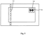
- Fig. 5 is a schematic structural diagram of a banknote.
- the banknote has the thin film element according to the embodiment of the present invention, and the thin film element is embedded within the banknote in the form of a window security thread 101.
- the thin film element is also used in the form of a sticker 102, and a perforated area 103 is provided in a substrate of the banknote for light transmission observation.
- the embodiment of the present invention is not limited to the security thread or the banknote, but is used in various thin film elements, for example in labels on goods and packaging, or in security documents, identity cards, passports, credit cards, health care cards, etc.
- a wide security bar or a transfer element may also be used, for example.
Landscapes
- Chemical & Material Sciences (AREA)
- Engineering & Computer Science (AREA)
- Organic Chemistry (AREA)
- Chemical Kinetics & Catalysis (AREA)
- Materials Engineering (AREA)
- Mechanical Engineering (AREA)
- Metallurgy (AREA)
- Theoretical Computer Science (AREA)
- General Physics & Mathematics (AREA)
- Physics & Mathematics (AREA)
- Health & Medical Sciences (AREA)
- Toxicology (AREA)
- Ceramic Engineering (AREA)
- Credit Cards Or The Like (AREA)
- Laminated Bodies (AREA)
Applications Claiming Priority (2)
| Application Number | Priority Date | Filing Date | Title |
|---|---|---|---|
| CN202110449714.0A CN115230277A (zh) | 2021-04-25 | 2021-04-25 | 薄膜元件、透明防伪元件、及数据载体 |
| PCT/CN2022/074032 WO2022227744A1 (zh) | 2021-04-25 | 2022-01-26 | 薄膜元件、透明防伪元件、及数据载体 |
Publications (4)
| Publication Number | Publication Date |
|---|---|
| EP4331840A1 true EP4331840A1 (de) | 2024-03-06 |
| EP4331840A4 EP4331840A4 (de) | 2024-07-24 |
| EP4331840B1 EP4331840B1 (de) | 2025-06-18 |
| EP4331840C0 EP4331840C0 (de) | 2025-06-18 |
Family
ID=83666022
Family Applications (1)
| Application Number | Title | Priority Date | Filing Date |
|---|---|---|---|
| EP22794225.7A Active EP4331840B1 (de) | 2021-04-25 | 2022-01-26 | Dünnschichtelement, transparentes fälschungssicheres element und datenträger |
Country Status (3)
| Country | Link |
|---|---|
| EP (1) | EP4331840B1 (de) |
| CN (1) | CN115230277A (de) |
| WO (1) | WO2022227744A1 (de) |
Family Cites Families (11)
| Publication number | Priority date | Publication date | Assignee | Title |
|---|---|---|---|---|
| US5549953A (en) * | 1993-04-29 | 1996-08-27 | National Research Council Of Canada | Optical recording media having optically-variable security properties |
| DE102007061979A1 (de) * | 2007-12-21 | 2009-06-25 | Giesecke & Devrient Gmbh | Sicherheitselement |
| DE102009008853A1 (de) * | 2009-02-13 | 2010-08-19 | Giesecke & Devrient Gmbh | Durchsichtssicherheitselement |
| DE102009041583A1 (de) * | 2009-09-15 | 2011-03-17 | Giesecke & Devrient Gmbh | Dünnschichtelement mit Interferenzschichtaufbau |
| DE102009058243A1 (de) * | 2009-12-14 | 2011-06-16 | Giesecke & Devrient Gmbh | Dünnschichtelement mit Mehrschichtstruktur |
| CN102401922B (zh) * | 2011-11-25 | 2014-10-08 | 天津科技大学 | 一种亚波长金属-介质光栅反射偏振光变膜及制作方法 |
| DE102012001121C5 (de) * | 2012-01-23 | 2018-01-04 | Leonhard Kurz Stiftung & Co. Kg | Sicherheitsdokument, Verfahren zur Herstellung eines Sicherheitsdokuments und Verfahren zur Herstellung eines individualisierten Sicherheitsdokuments |
| GB201301788D0 (en) * | 2013-02-01 | 2013-03-20 | Rue De Int Ltd | Security devices and methods of manufacture thereof |
| DE102015005446A1 (de) * | 2015-04-28 | 2016-11-03 | Giesecke & Devrient Gmbh | Sicherheitselement mit Mehrschichtstruktur |
| DE102015014505A1 (de) * | 2015-11-10 | 2017-05-11 | Giesecke & Devrient Gmbh | Sicherheitselement, Verfahren zum Herstellen desselben und mit dem Sicherheitselement ausgestatteter Datenträger |
| DE102016007649A1 (de) * | 2016-06-22 | 2017-12-28 | Giesecke+Devrient Currency Technology Gmbh | Optisch variables Sicherheitselement |
-
2021
- 2021-04-25 CN CN202110449714.0A patent/CN115230277A/zh active Pending
-
2022
- 2022-01-26 WO PCT/CN2022/074032 patent/WO2022227744A1/zh not_active Ceased
- 2022-01-26 EP EP22794225.7A patent/EP4331840B1/de active Active
Also Published As
| Publication number | Publication date |
|---|---|
| EP4331840B1 (de) | 2025-06-18 |
| EP4331840A4 (de) | 2024-07-24 |
| CN115230277A (zh) | 2022-10-25 |
| WO2022227744A1 (zh) | 2022-11-03 |
| EP4331840C0 (de) | 2025-06-18 |
Similar Documents
| Publication | Publication Date | Title |
|---|---|---|
| CN102652064B (zh) | 具有多层结构的金色薄膜元件 | |
| RU2514589C2 (ru) | Тонкопленочный элемент с интерференционной слоистой структурой | |
| US9701151B2 (en) | Security thread | |
| AU723787B2 (en) | Security device | |
| EP3774373B1 (de) | Optische vorrichtung und verfahren zur herstellung davon | |
| CN103370206A (zh) | 安全元件和安全元件的制造方法 | |
| EP3643511A1 (de) | Sicherheitselement und mit dem sicherheitselement ausgestatteter datenträger | |
| EP3687828B9 (de) | Sicherheitsvorrichtung und verfahren zur herstellung davon | |
| US7699351B2 (en) | Security document with a volume hologram forming a partial motif | |
| EP4039491B1 (de) | Fälschungssicheres optisches element und fälschungssicheres optisches produkt | |
| WO2010121293A1 (en) | Optically variable device and security document including same | |
| US20200130396A1 (en) | A security device and method of making thereof | |
| JP7496837B2 (ja) | プラズモン効果を有する光学セキュリティコンポーネント、そのようなコンポーネントの製造、そのようなコンポーネントを備えたセキュリティオブジェクト | |
| EP4331840A1 (de) | Dünnschichtelement, transparentes fälschungssicheres element und datenträger | |
| US20230073096A1 (en) | An Optical Effect Device | |
| Baloukas et al. | Optical coatings for security and authentication devices | |
| van Renesse | Ordering the order: a survey of optical document security features | |
| RU2374080C1 (ru) | Защитный элемент на основе многослойной прозрачной цветоконтрастной разрушаемой полимерной структуры для защищенного полиграфического изделия, способ его получения, защищенный от подделки материал и полиграфическое изделие | |
| CN108349291A (zh) | 防伪元件和设有该防伪元件的数据载体 | |
| WO2025141099A1 (en) | Method for producing data carrier and data carrier produced thereof | |
| WO2022144258A1 (en) | Security element for documents, particularly banknotes, and method for its production |
Legal Events
| Date | Code | Title | Description |
|---|---|---|---|
| STAA | Information on the status of an ep patent application or granted ep patent |
Free format text: STATUS: THE INTERNATIONAL PUBLICATION HAS BEEN MADE |
|
| PUAI | Public reference made under article 153(3) epc to a published international application that has entered the european phase |
Free format text: ORIGINAL CODE: 0009012 |
|
| STAA | Information on the status of an ep patent application or granted ep patent |
Free format text: STATUS: REQUEST FOR EXAMINATION WAS MADE |
|
| 17P | Request for examination filed |
Effective date: 20231123 |
|
| AK | Designated contracting states |
Kind code of ref document: A1 Designated state(s): AL AT BE BG CH CY CZ DE DK EE ES FI FR GB GR HR HU IE IS IT LI LT LU LV MC MK MT NL NO PL PT RO RS SE SI SK SM TR |
|
| A4 | Supplementary search report drawn up and despatched |
Effective date: 20240626 |
|
| RIC1 | Information provided on ipc code assigned before grant |
Ipc: B32B 27/36 20060101AFI20240620BHEP |
|
| DAV | Request for validation of the european patent (deleted) | ||
| DAX | Request for extension of the european patent (deleted) | ||
| GRAP | Despatch of communication of intention to grant a patent |
Free format text: ORIGINAL CODE: EPIDOSNIGR1 |
|
| STAA | Information on the status of an ep patent application or granted ep patent |
Free format text: STATUS: GRANT OF PATENT IS INTENDED |
|
| INTG | Intention to grant announced |
Effective date: 20250218 |
|
| GRAS | Grant fee paid |
Free format text: ORIGINAL CODE: EPIDOSNIGR3 |
|
| GRAA | (expected) grant |
Free format text: ORIGINAL CODE: 0009210 |
|
| STAA | Information on the status of an ep patent application or granted ep patent |
Free format text: STATUS: THE PATENT HAS BEEN GRANTED |
|
| AK | Designated contracting states |
Kind code of ref document: B1 Designated state(s): AL AT BE BG CH CY CZ DE DK EE ES FI FR GB GR HR HU IE IS IT LI LT LU LV MC MK MT NL NO PL PT RO RS SE SI SK SM TR |
|
| REG | Reference to a national code |
Ref country code: GB Ref legal event code: FG4D |
|
| REG | Reference to a national code |
Ref country code: CH Ref legal event code: EP |
|
| REG | Reference to a national code |
Ref country code: DE Ref legal event code: R096 Ref document number: 602022016197 Country of ref document: DE |
|
| REG | Reference to a national code |
Ref country code: CH Ref legal event code: EP |
|
| REG | Reference to a national code |
Ref country code: IE Ref legal event code: FG4D |
|
| U01 | Request for unitary effect filed |
Effective date: 20250620 |
|
| U07 | Unitary effect registered |
Designated state(s): AT BE BG DE DK EE FI FR IT LT LU LV MT NL PT RO SE SI Effective date: 20250711 |
|
| PG25 | Lapsed in a contracting state [announced via postgrant information from national office to epo] |
Ref country code: GR Free format text: LAPSE BECAUSE OF FAILURE TO SUBMIT A TRANSLATION OF THE DESCRIPTION OR TO PAY THE FEE WITHIN THE PRESCRIBED TIME-LIMIT Effective date: 20250919 Ref country code: NO Free format text: LAPSE BECAUSE OF FAILURE TO SUBMIT A TRANSLATION OF THE DESCRIPTION OR TO PAY THE FEE WITHIN THE PRESCRIBED TIME-LIMIT Effective date: 20250918 |
|
| PG25 | Lapsed in a contracting state [announced via postgrant information from national office to epo] |
Ref country code: HR Free format text: LAPSE BECAUSE OF FAILURE TO SUBMIT A TRANSLATION OF THE DESCRIPTION OR TO PAY THE FEE WITHIN THE PRESCRIBED TIME-LIMIT Effective date: 20250618 |
|
| PG25 | Lapsed in a contracting state [announced via postgrant information from national office to epo] |
Ref country code: RS Free format text: LAPSE BECAUSE OF FAILURE TO SUBMIT A TRANSLATION OF THE DESCRIPTION OR TO PAY THE FEE WITHIN THE PRESCRIBED TIME-LIMIT Effective date: 20250918 |
|
| PG25 | Lapsed in a contracting state [announced via postgrant information from national office to epo] |
Ref country code: IS Free format text: LAPSE BECAUSE OF FAILURE TO SUBMIT A TRANSLATION OF THE DESCRIPTION OR TO PAY THE FEE WITHIN THE PRESCRIBED TIME-LIMIT Effective date: 20251018 |
|
| PG25 | Lapsed in a contracting state [announced via postgrant information from national office to epo] |
Ref country code: SM Free format text: LAPSE BECAUSE OF FAILURE TO SUBMIT A TRANSLATION OF THE DESCRIPTION OR TO PAY THE FEE WITHIN THE PRESCRIBED TIME-LIMIT Effective date: 20250618 |
|
| PG25 | Lapsed in a contracting state [announced via postgrant information from national office to epo] |
Ref country code: CZ Free format text: LAPSE BECAUSE OF FAILURE TO SUBMIT A TRANSLATION OF THE DESCRIPTION OR TO PAY THE FEE WITHIN THE PRESCRIBED TIME-LIMIT Effective date: 20250618 |
|
| PG25 | Lapsed in a contracting state [announced via postgrant information from national office to epo] |
Ref country code: PL Free format text: LAPSE BECAUSE OF FAILURE TO SUBMIT A TRANSLATION OF THE DESCRIPTION OR TO PAY THE FEE WITHIN THE PRESCRIBED TIME-LIMIT Effective date: 20250618 |
|
| PG25 | Lapsed in a contracting state [announced via postgrant information from national office to epo] |
Ref country code: SK Free format text: LAPSE BECAUSE OF FAILURE TO SUBMIT A TRANSLATION OF THE DESCRIPTION OR TO PAY THE FEE WITHIN THE PRESCRIBED TIME-LIMIT Effective date: 20250618 |
|
| PG25 | Lapsed in a contracting state [announced via postgrant information from national office to epo] |
Ref country code: ES Free format text: LAPSE BECAUSE OF FAILURE TO SUBMIT A TRANSLATION OF THE DESCRIPTION OR TO PAY THE FEE WITHIN THE PRESCRIBED TIME-LIMIT Effective date: 20250618 |
|
| U20 | Renewal fee for the european patent with unitary effect paid |
Year of fee payment: 5 Effective date: 20260130 |
|
| PLBE | No opposition filed within time limit |
Free format text: ORIGINAL CODE: 0009261 |
|
| STAA | Information on the status of an ep patent application or granted ep patent |
Free format text: STATUS: NO OPPOSITION FILED WITHIN TIME LIMIT |
|
| REG | Reference to a national code |
Ref country code: CH Ref legal event code: L10 Free format text: ST27 STATUS EVENT CODE: U-0-0-L10-L00 (AS PROVIDED BY THE NATIONAL OFFICE) Effective date: 20260430 |