EP4332740A2 - Anzeigevorrichtung und tragbares endgerät damit - Google Patents
Anzeigevorrichtung und tragbares endgerät damit Download PDFInfo
- Publication number
- EP4332740A2 EP4332740A2 EP24150051.1A EP24150051A EP4332740A2 EP 4332740 A2 EP4332740 A2 EP 4332740A2 EP 24150051 A EP24150051 A EP 24150051A EP 4332740 A2 EP4332740 A2 EP 4332740A2
- Authority
- EP
- European Patent Office
- Prior art keywords
- touch
- sensor
- signal lines
- disposed
- parts
- Prior art date
- Legal status (The legal status is an assumption and is not a legal conclusion. Google has not performed a legal analysis and makes no representation as to the accuracy of the status listed.)
- Pending
Links
Images







Classifications
-
- G—PHYSICS
- G06—COMPUTING OR CALCULATING; COUNTING
- G06F—ELECTRIC DIGITAL DATA PROCESSING
- G06F3/00—Input arrangements for transferring data to be processed into a form capable of being handled by the computer; Output arrangements for transferring data from processing unit to output unit, e.g. interface arrangements
- G06F3/01—Input arrangements or combined input and output arrangements for interaction between user and computer
- G06F3/03—Arrangements for converting the position or the displacement of a member into a coded form
- G06F3/041—Digitisers, e.g. for touch screens or touch pads, characterised by the transducing means
- G06F3/0412—Digitisers structurally integrated in a display
-
- G—PHYSICS
- G06—COMPUTING OR CALCULATING; COUNTING
- G06F—ELECTRIC DIGITAL DATA PROCESSING
- G06F3/00—Input arrangements for transferring data to be processed into a form capable of being handled by the computer; Output arrangements for transferring data from processing unit to output unit, e.g. interface arrangements
- G06F3/01—Input arrangements or combined input and output arrangements for interaction between user and computer
- G06F3/03—Arrangements for converting the position or the displacement of a member into a coded form
- G06F3/033—Pointing devices displaced or positioned by the user, e.g. mice, trackballs, pens or joysticks; Accessories therefor
- G06F3/0354—Pointing devices displaced or positioned by the user, e.g. mice, trackballs, pens or joysticks; Accessories therefor with detection of two-dimensional [2D] relative movements between the device, or an operating part thereof, and a plane or surface, e.g. 2D mice, trackballs, pens or pucks
- G06F3/03545—Pens or stylus
-
- G—PHYSICS
- G06—COMPUTING OR CALCULATING; COUNTING
- G06F—ELECTRIC DIGITAL DATA PROCESSING
- G06F3/00—Input arrangements for transferring data to be processed into a form capable of being handled by the computer; Output arrangements for transferring data from processing unit to output unit, e.g. interface arrangements
- G06F3/01—Input arrangements or combined input and output arrangements for interaction between user and computer
- G06F3/03—Arrangements for converting the position or the displacement of a member into a coded form
- G06F3/033—Pointing devices displaced or positioned by the user, e.g. mice, trackballs, pens or joysticks; Accessories therefor
- G06F3/038—Control and interface arrangements therefor, e.g. drivers or device-embedded control circuitry
-
- G—PHYSICS
- G06—COMPUTING OR CALCULATING; COUNTING
- G06F—ELECTRIC DIGITAL DATA PROCESSING
- G06F3/00—Input arrangements for transferring data to be processed into a form capable of being handled by the computer; Output arrangements for transferring data from processing unit to output unit, e.g. interface arrangements
- G06F3/01—Input arrangements or combined input and output arrangements for interaction between user and computer
- G06F3/03—Arrangements for converting the position or the displacement of a member into a coded form
- G06F3/041—Digitisers, e.g. for touch screens or touch pads, characterised by the transducing means
- G06F3/044—Digitisers, e.g. for touch screens or touch pads, characterised by the transducing means by capacitive means
-
- G—PHYSICS
- G06—COMPUTING OR CALCULATING; COUNTING
- G06F—ELECTRIC DIGITAL DATA PROCESSING
- G06F3/00—Input arrangements for transferring data to be processed into a form capable of being handled by the computer; Output arrangements for transferring data from processing unit to output unit, e.g. interface arrangements
- G06F3/01—Input arrangements or combined input and output arrangements for interaction between user and computer
- G06F3/03—Arrangements for converting the position or the displacement of a member into a coded form
- G06F3/041—Digitisers, e.g. for touch screens or touch pads, characterised by the transducing means
- G06F3/044—Digitisers, e.g. for touch screens or touch pads, characterised by the transducing means by capacitive means
- G06F3/0445—Digitisers, e.g. for touch screens or touch pads, characterised by the transducing means by capacitive means using two or more layers of sensing electrodes, e.g. using two layers of electrodes separated by a dielectric layer
-
- G—PHYSICS
- G06—COMPUTING OR CALCULATING; COUNTING
- G06F—ELECTRIC DIGITAL DATA PROCESSING
- G06F3/00—Input arrangements for transferring data to be processed into a form capable of being handled by the computer; Output arrangements for transferring data from processing unit to output unit, e.g. interface arrangements
- G06F3/01—Input arrangements or combined input and output arrangements for interaction between user and computer
- G06F3/03—Arrangements for converting the position or the displacement of a member into a coded form
- G06F3/041—Digitisers, e.g. for touch screens or touch pads, characterised by the transducing means
- G06F3/044—Digitisers, e.g. for touch screens or touch pads, characterised by the transducing means by capacitive means
- G06F3/0446—Digitisers, e.g. for touch screens or touch pads, characterised by the transducing means by capacitive means using a grid-like structure of electrodes in at least two directions, e.g. using row and column electrodes
-
- H—ELECTRICITY
- H10—SEMICONDUCTOR DEVICES; ELECTRIC SOLID-STATE DEVICES NOT OTHERWISE PROVIDED FOR
- H10K—ORGANIC ELECTRIC SOLID-STATE DEVICES
- H10K59/00—Integrated devices, or assemblies of multiple devices, comprising at least one organic light-emitting element covered by group H10K50/00
- H10K59/40—OLEDs integrated with touch screens
-
- G—PHYSICS
- G06—COMPUTING OR CALCULATING; COUNTING
- G06F—ELECTRIC DIGITAL DATA PROCESSING
- G06F2203/00—Indexing scheme relating to G06F3/00 - G06F3/048
- G06F2203/041—Indexing scheme relating to G06F3/041 - G06F3/045
- G06F2203/04103—Manufacturing, i.e. details related to manufacturing processes specially suited for touch sensitive devices
-
- G—PHYSICS
- G06—COMPUTING OR CALCULATING; COUNTING
- G06F—ELECTRIC DIGITAL DATA PROCESSING
- G06F2203/00—Indexing scheme relating to G06F3/00 - G06F3/048
- G06F2203/041—Indexing scheme relating to G06F3/041 - G06F3/045
- G06F2203/04106—Multi-sensing digitiser, i.e. digitiser using at least two different sensing technologies simultaneously or alternatively, e.g. for detecting pen and finger, for saving power or for improving position detection
-
- G—PHYSICS
- G06—COMPUTING OR CALCULATING; COUNTING
- G06F—ELECTRIC DIGITAL DATA PROCESSING
- G06F2203/00—Indexing scheme relating to G06F3/00 - G06F3/048
- G06F2203/041—Indexing scheme relating to G06F3/041 - G06F3/045
- G06F2203/04107—Shielding in digitiser, i.e. guard or shielding arrangements, mostly for capacitive touchscreens, e.g. driven shields, driven grounds
Definitions
- the present disclosure herein relates generally to a portable terminal, and more particularly, to a portable terminal including a display device.
- Electronic apparatuses such as smartphones, laptop computers, and smart televisions have been developed. Such electronic devices are provided with display devices to provide information.
- Some recent display devices may include a touch detection function capable of interacting with users in addition to its image display function.
- the touch detecting function determines whether and where an object touches a screen when a user's finger, a touch pen, or the like contacts or approaches the screen.
- the display device may receive an image signal on the basis of such touch coordinates.
- Embodiments of the present disclosure provide a display device including a touch sensing unit in which connection parts connecting sensor parts are disposed adjacent to a peripheral region in an active region, and a portable terminal including the same.
- Embodiments of the present disclosure also provide a display device including a blocking electrode which prevents electrical coupling between the sensor parts and signal lines, and a portable terminal including the same.
- An embodiment of the inventive concept provides a display device including: a display panel including an active region and a peripheral region adjacent to the active region; n first touch sensors which are arranged successively along a first direction and extend in a second direction, each of the n first touch sensors including a plurality of first connecting parts and a plurality of first sensor parts connected through the first connecting parts, and configured to generate an electric field together with an external touch pen; m second touch sensors which are insulated from the n first touch sensors, extend in the first direction, and are arranged successively along the second direction, each of the m second touch sensors including a plurality of second connecting parts and a plurality of second sensor parts connected through the second connecting parts, and being configured to generate an electric field together with the external touch pen; and a plurality of signal lines configured to transmit a detection signal for detecting an input point of the touch pen to the n first touch sensors and the m second touch sensors, wherein the first sensor parts of the first touch sensor and the nth first touch sensor, which are disposed adjacent to the peripheral region
- the display device may further include a blocking electrode disposed in the peripheral region, wherein ends of the signal lines may be respectively connected to the n first touch sensors and the m second touch sensors, and the blocking electrode may be disposed adjacent to the one ends of the signal lines connected to the first and second touch sensors.
- the signal lines may include a plurality of first to fourth signal lines, wherein ends of the first signal lines may be respectively connected to ends of the n first touch sensors, ends of the second signal lines may be respectively connected to the other ends of the n first touch sensors; ends of the third signal lines may be respectively connected to ends of the m second touch sensors, and ends of the fourth signal lines may be respectively connected to other ends of the m n second touch sensors.
- the blocking electrode may be disposed in the peripheral region and adjacent to ends of the first to fourth signal lines so as to surround the active region.
- ends of the signal lines may be respectively connected to the first and second connecting parts.
- the first connecting parts and the signal lines may be directly disposed on the display panel.
- the first sensor parts, the second sensor parts, the second connecting parts, and the blocking electrode may be disposed on a layer different from a layer on which the first connecting parts and the signal lines are disposed.
- a first insulating layer may be disposed on the first connecting parts and the signal lines, and the first sensor parts, the second sensor parts and the second connecting parts may be disposed on the first insulating part.
- the first sensor parts, the second sensor parts, the second connecting parts and the blocking electrode may be directly disposed on the display panel.
- the first connecting parts and the signal lines may be disposed on a layer different from on which the first sensor parts, the second sensor parts, the second connecting parts, and the blocking electrode are disposed.
- the display panel may include: a base substrate; a plurality of organic light-emitting elements disposed on the base substrate; and an encapsulating substrate encapsulating the organic light-emitting elements and disposed on the base substrate, wherein the n first touch sensors and the m second touch sensors may be disposed on the encapsulating substrate.
- An embodiment of the inventive concept provides a portable terminal including: a display device and a touch pen for selecting information displayed on the display device, the display device including: a display panel including an active region and a peripheral region adjacent to the active region; n first touch sensors arranged in a first direction and extending in a second direction, each of the n first touch sensors including a plurality of first connecting parts and a plurality of first sensor parts connected through the first connecting parts, the plurality of first sensor parts being configured to generate an electric field with an external touch pen; m second touch sensors insulated from the n first touch sensors, extending in the first direction, and arranged successively along the second direction, each of the m first touch sensors including a plurality of second connecting parts and a plurality of second sensor parts connected through the second connecting parts, the plurality of second sensor parts being configured to generate an electric field with an external touch pen; and a plurality of signal lines configured to transmit a detection signal for detecting an input point of the touch pen to the n first touch sensors and the m second touch sensors,
- the display device may further include a blocking electrode disposed in the peripheral region, wherein ends of the signal lines may be respectively connected to the n first touch sensors and the m second touch sensors, and the blocking electrode may be disposed adjacent to the ends of the signal lines connected to the first and second touch sensors.
- the first connecting parts and the signal lines may be directly disposed on the display panel.
- the first sensor parts, the second sensor parts, the second connecting parts, and the blocking electrode may be disposed on a layer different from a layer on which the first connecting parts and the signal lines are disposed.
- the touch pen may include a detecting part for contacting a touch coordinate of the display device, wherein the detecting part may be configured to generate an electric field with each of the n first touch sensors and the m second touch sensors.
- the detecting part may include a metal.
- 'include' or 'comprise' specifies a property, a region, a fixed number, a step, a process, an element and/or a component but does not exclude other properties, regions, fixed numbers, steps, processes, elements and/or components. All numerical values are approximate, and may vary. All examples of specific materials and compositions are to be taken as nonlimiting and exemplary only. Other suitable materials and compositions may be used instead.
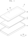
- FIG. 1 is a block diagram of a portable terminal according to an embodiment of the inventive concept.
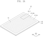
- FIG. 2A is a plan view of a display panel illustrated in FIG. 1 .
- FIG. 2B is an equivalent circuit diagram of one pixel illustrated in FIG. 2A .
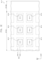
- FIG. 2C is a partial plan view of a display panel illustrated in FIG. 2A .
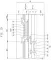
- FIG. 2D is a partial plan view of a display panel illustrated in FIG. 2A .
- the portable terminal DD illustrated in FIG. 1 may be applied to tablet PCs, smartphones, personal digital assistants (PDAs), portable multimedia players (PMPs), game consoles, wrist watch type electronic apparatuses, and the like. These are merely examples and embodiments may, of course, be applied to other electronic devices.
- the portable terminal DD may be a display device.
- the portable terminal DD will be described as a display device DD.
- the display device DD includes a display area DA on which an image is displayed and a non-display area NDA adjacent to the display area DA.
- the non-display area NDA may surround the display area DA.
- the display device DD may include a window member WM, a display panel DP, a touch sensing unit TS, and a receiving member BC.
- the window member WM is disposed over the touch sensing unit TS, and may transmit an image provided from the display panel DP through the display region DA.
- the window member may be configured from glass, sapphire, plastic, or the like.
- the window member WM may include a plurality of layers.
- the window member WM may include at least one bezel layer disposed on a lower surface of a supporting layer.
- the display panel DP may be a liquid crystal display panel, an organic light-emitting display panel, an elctrophoretic display panel, an electrowetting display panel, or the like, and the type thereof is not limited.
- an organic light-emitting display panel is exemplarily described.
- the display panel DP is parallel to a surface defined by a first direction DR1 and a second direction DR2.
- the normal direction to the display panel DP is indicated by a third direction DR3.
- the third direction DR3 indicates the thickness direction of the display device DD.
- the front surfaces (or upper surfaces) and the lower surfaces (or rear surfaces) of members are distinguished by the third direction DR3.
- the directions indicated by the first to third directions DR1, DR2 and DR3 are relative concepts and may be converted into other directions.
- the display panel DP may include a lower substrate DS and an upper substrate US.
- a plurality of pixels PX, a plurality of organic light-emitting elements OLED, and a plurality of signal lines required to drive the display device DD may be disposed.
- the signal lines include a plurality of gate lines which extend in the second direction DR2 and are arranged in the first direction DR1.
- the signal lines may include a plurality of data lines which extend in the first direction DR1 and are arranged in the second direction DR2.
- the gate lines and the data lines respectively cross each other in an insulative manner.
- the embodiment of the inventive concept is not limited thereto, and the gate lines may extend in the first direction DR1 and be arranged successively along the second direction DR2.
- the data lines may extend in the second direction DR2 and be arranged successively along the first direction DR1.
- the upper substrate US is disposed on the lower substrate DS and encapsulates the organic light-emitting elements OLED included in the lower substrate DS from the outside.
- the upper substrate US may be provided as an encapsulating substrate TFE (see FIG. 2D ).
- the display panel DP when viewed in plan view, may include a display region DP-DA and a non-display region DP-NDA.
- the display region DP-DA and the non-display region DP-NDA may have various shapes and configurations according to the structure and design of the display panel DP.
- Pixels PX may be disposed in a matrix shape so as to overlap the display region DP-DA.
- the embodiment of the inventive concept is not limited thereto.
- the pixels PX may be disposed in a non-matrix shape, for example, in a PenTile shape.
- FIG. 2B an equivalent circuit of a pixel PXii connected to an ith gate line SLi and a jth data line DLi is exemplarily illustrated.
- the pixel PXii includes a first thin film transistor TR1, a second thin film transistor TR2, a capacitor CAP, and an organic light-emitting element OLEDij.
- the first thin film transistor TR1 includes a control electrode connected to the ith scan line SLi, an input electrode connected to a jth data line DLj, and an output electrode.
- the first transistor TR1 outputs a data signal applied to the jth source line DLj in response to a gate signal applied to the ith scan line SLi.
- the capacitor CAP includes a first capacitor electrode connected to the first thin film transistor TR1, and a second capacitor electrode receiving a first power supply voltage ELVDD.
- the capacitor CAP charges an amount of charge corresponding to the difference between a voltage corresponding to a data signal received from the first thin film transistor TR1 and the first power supply voltage ELVDD.
- the second thin film transistor TR2 includes: a control electrode connected to the output electrode of the first thin film transistor TR1 and the first capacitor electrode of the capacitor CAP; an input electrode receiving the first power supply voltage ELVDD, and an output electrode.
- the output electrode of the second thin film transistor TR2 is connected to the organic light-emitting element OLEDij.
- the second thin film transistor TR2 controls driving current flowing through the organic light emitting element OLEDij corresponding to the amount of charge stored in the capacitor CAP. More specifically, a turn-on time of the second thin film transistor TR2 is determined according to the amount of charge charged in the capacitor CAP. Substantially, the output electrode of the second thin film transistor TR2 provides the organic light-emitting element OLEDij with a voltage with a level lower than that of the first power supply voltage ELVDD.
- the organic light emitting element OLEDij includes a first electrode connected to the second thin film transistor TR2, and a second electrode receiving a second power supply voltage ELVSS.
- the organic light emitting element OLEDij may include a light-emitting pattern disposed between the first and second electrodes.
- the organic light emitting element OLEDij emits light during a turn-on interval of the second thin film transistor TR2.
- the colour of light generated in the organic light emitting element OLEDij is determined by a material constituting the light-emitting pattern.
- the colour of light generated in the organic light emitting element OLEDij may be any one of red, green, blue or white.
- the display region DP-DA is defined as a plurality of light-emitting regions EA-R, EA-G and EA-B and non-light-emitting region NEA in a plane defined by the first and second directions DR1 and DR2.
- FIG. 2C exemplarily illustrates three types of light-emitting regions EA-R, EA-G and EA-B which are disposed in a matrix shape. Three organic light-emitting elements which emit colours different from each other in the three types of light-emitting regions EA-R, EA-G and EA-B.
- organic light-emitting elements which emit white colours are present in the three types of light-emitting regions EA-R, EA-G and EA-B.
- colour filters of three types of colours different from each other may respectively overlap three types of light-emitting regions EA-R, EA-G and EA-B.
- the wording "light having a predetermined colour is emitted from the light-emitting region" may include not only the case in which light generated from the corresponding light-emitting element is emitted without conversion to a different colour, but also the feature in which the colour of light generated from the corresponding light-emitting element is converted and then emitted.
- a plurality of light-emitting regions EA-R, EA-G and EA-B may include four or more types of light-emitting regions.
- the non-light-emitting region NEA may be divided into first non-light-emitting regions NEA-1 surrounding light-emitting regions EA-R, EA-G and EA-B and second non-light-emitting regions NEA-2 defining a border of the first non-light-emitting regions NEA-1.
- a driving circuit for example the thin film transistors TFT1 and TFT2 (see FIG. 2B ) or the capacitor CAP (see FIG. 2B ), may be disposed in each of the first non-light-emitting regions NEA-1.
- signal lines for example the gate line SLi (see FIG. 2B ) and the data line DLi (see FIG. 2B ), may be disposed.
- the embodiment of the inventive concept is not limited thereto, and the first non-light emitting region NEA-1 and the second non-light emitting regions NEA-2 may not be separated from each other.
- the light-emitting regions EA-R, EA-G and EA-B each may have a shape similar to a rhombus.
- organic light-emitting elements emitting four colours different from each other may be respectively disposed in four types of light-emitting regions that form a repeating pattern.
- FIG. 2D a partial cross-sectional view of the display panel DP illustrated in FIG. 2A is illustrated.
- the region including second thin film transistor TR2 illustrated in FIG. 2B is exemplarily described.
- the display panel DP includes a base substrate SUB, a circuit layer DP-CL, a light-emitting element layer DP-OLED and an encapsulating substrate TFE.
- the base substrate SUB may be the lower substrate DS illustrated in FIG. 2A
- the encapsulating substrate TFE may be the upper substrate US.
- the base substrate SUB may include a plastic substrate, a glass substrate, a metal substrate, an organic/inorganic composite material substrate, or the like.
- the base substrate SUB may have a multilayer structure.
- the circuit layer DP-CL may include a plurality of conductive layers and a plurality of insulating layers
- the organic light-emitting element layer DP-OLED may include a plurality of conductive layers and a plurality of functional organic layers.
- a semiconductor pattern AL of the thin film transistors TR2 is disposed on the base substrate SUB.
- a first insulating layer 12 for covering the semiconductor pattern AL is disposed on the base substrate SUB.
- the first insulating layer 12 includes an organic and/or inorganic layer.
- a control electrode GE of the transistor TR2 is disposed on the first insulating layer 12.
- a second insulating layer 14 for covering the control electrode GE is disposed on the first insulating layer 12.
- the second insulating layer 14 includes an organic and/or inorganic layer.
- An input electrode SE and an output electrode DE of the second thin film transistor TR2 are disposed on the second insulating layer 14.
- the input electrode SE is branched from the data line DLi.
- the output electrodes DE is branched from a power line PWL.
- the input electrode SE and the output electrode DE are respectively connected to the semiconductor pattern AL through a first through hole CH1 and a second through hole CH2 which penetrate through the first insulating layer 12 and the second insulating layer 14.
- the second thin film transistor TR2 may be implemented with a bottom gate structure
- a third insulating layer 16 covering the input electrode SE and the output electrode DE is disposed on the second insulating layer 14.
- the third insulating layer 16 includes an organic and/or inorganic layer.
- the third insulating layer 16 may include an organic material to provide a flat surface.
- a pixel defining film PXL and the organic light-emitting diode OLED are disposed on the third insulating layer 16.
- An opening part OP is defined in the pixel defining film PXL.
- the pixel defining film PXL serves as another insulating layer.
- the opening OP of FIG. 2D may correspond to opening parts OP-R, OP-G and OP-B of FIG. 2C .
- the anode AE is connected to the output electrode DE through a third through hole CH3 penetrating through the third insulating layer 16.
- the opening part OP of the pixel defining film PXL exposes at least a portion of the anode AE.
- a hole control layer HCL may be provided in common in the light-emitting regions EA-R, EA-G, and EA-B and the non-light-emitting region NPXA.
- An organic light-emitting layer EML and an electron control layer ECL are sequentially formed on the hole control layer HCL.
- the hole control layer HCL includes at least a hole transport layer, and the electron control layer ECL includes at least an electron transporting layer.
- a cathode CE may be formed in common in the light-emitting regions EAA-R, EA-G and EA-B, and the non-light-emitting region NEA.
- An encapsulating substrate TFE for encapsulating the organic light-emitting element layer DP-OLED is disposed on the cathode CE.
- the encapsulating substrate TFE may be attached to the base substrate SUB through a sealing material.
- a thin film encapsulating substrate covering the organic light-emitting element layer DP-OLED may instead be disposed on the cathode CE.
- the thin film encapsulating substrate includes at least two inorganic thin films and organic thin films disposed between the inorganic thin films. The inorganic thin films protect the organic light-emitting element OLED from water, and the organic thin films protect the organic light-emitting element OLED from foreign substances such as dust particles.
- the touch sensing unit TS may be disposed between the display panel DP and the window member WM to detect coordinate information for an external touch.
- the touch sensing unit TS may be provided as electrostatic capacitive type touch sensors.
- the embodiment of the inventive concept is not limited thereto, and may include touch sensing units of any one or more other types, including electromagnetic induction type or other touch electrodes.
- the receiving member BC is coupled to a window member WM so as to receive the display panel DP.
- the receiving member BC may be formed as a plurality of portions that are assembled together, or may include one unitary body which is injection molded.
- the receiving member BC may include a plastic or metal.
- the display device DD is illustrated as being flat in FIG. 1 , the display device DD according to the inventive concept may be implemented as a flexible display device. That is, components such as the display panel DP and the window member WM may include flexible materials and may be bent, extended or pressed.
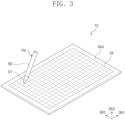
- FIG. 3 is a view illustrating a touch sensing unit and a pen according to an embodiment of the inventive concept.
- FIG. 4 is a cross-sectional view of the touch sensing unit illustrated in FIG. 3 .
- a touch sensing unit TS may include an active region AA and a peripheral region NAA.
- the active region AA may correspond to the display region DP-DA of the display panel DP illustrated in FIG. 2
- the peripheral region may correspond to the non-display region DP-NDA of the display panel DP.
- the peripheral region NAA is defined as being adjacent to the active region AA.
- the peripheral region NAA may have a frame shape surrounding the active region AA.
- the touch sensing unit TS does not detect an external touch applied to the peripheral region NAA.
- the touch detecting unit TS may include a first conductive layer TS-CL1, a first insulating layer TS-IL1, a second conductive layer TS-CL2, and a second insulating layer TS-IL2.
- Each of the first conductive layer TS-CL1 and the second conductive layer TS-CL2 may have a single layer structure or may have a multilayer structure successively laminated in a third direction DR3.
- the multilayer-structured conductive layer may have at least one metal layer.
- the multilayer-structured conductive layer may include metal layers with differing conductors, i.e. transparent conductors and/or metals.
- the transparent conductive layers may include indium tin oxide (ITO), indium zinc oxide (IZO), zinc oxide (ZnO), indium tin zinc oxide (ITZO), PEDOT, metal nanowires, or graphene.
- the metal layers may include molybdenum, silver, titanium, copper, aluminum, and alloys thereof.
- Each of the first conductive layer TS-CL1 and the second conductive layer TS-CL2 includes a plurality of patterns.
- the first conductive layer TS-CL1 includes first conductive patterns
- the second conductive layer TS-CL2 includes second conductive patterns.
- Each of the first conductive patterns and the second conductive patterns may include a touch electrode and touch signal lines.
- Each of the first insulating layer TS-IL1 and the second insulating layer TS-IL2 may include an inorganic or organic material.
- the inorganic material may include silicon oxide or silicon nitride.
- the organic material may include at least any one of an acryl-based resin, a methacryl-based resin, a polyisoprene-based resin, an epoxy-based resin, a urethane-based resin, a cellulose-based resin, or parylene-based resin.
- the first insulating layer TS-IL1 insulates the first conductive layer TS-CL1 from the second conductive layer TS-CL2, and the shape thereof is not limited. According to the shapes of the first conductive patterns and the second conductive patterns, the shape of the first insulating layer TS-IL1 may be changed.
- the first insulating layer TS-IL1 may entirely cover the encapsulating substrate TFE (see FIG. 2D ) or include a plurality of insulating patterns.
- a two-layered electrostatic capacitive touch screen is exemplarily illustrated.
- the touch sensing unit TS may be driven through a self-capacitance method, and the method for driving a touch screen for obtaining coordinate information is not particularly limited.
- the touch sensing unit TS may detect a touch coordinate on the basis of the movement of a touch pen PN.
- the touch pen PN includes a body part BD and detection part DT connected to an end of the body part BD.
- the body part BD may include a power supply part and provide power to the detecting part DT of the touch pen PN.
- the detecting part DT may correspond to a general pen point and may be provided as a conductor such as a metal.
- the detecting part DT may respond to power provided from the body part BD and may thus generate an electric field with surrounding metallic objects.
- the touch sensing unit TS In operation, when the touch pen PN contacts or approaches the touch sensing unit TS, a touch coordinate is detected by the touch sensing unit TS, but the embodiment of the inventive concept is not limited thereto.
- the contact may include both a touch and an approach between two objects. That is, the touch sensing unit TS according to the inventive concept may recognize the touch coordinate by means of not only the touch pen PN but also various methods such as a contact of a user's body.
- the detecting part DT may generate an electric field to trigger sensors included in the touch sensing unit TS.
- the magnitudes of voltages provided to the detecting part DT and to the touch sensors may be different from each other.
- a voltage difference may be generated. Due to such voltage difference, an electric field may be generated between the detecting part DT and the touch sensors.
- the touch sensing unit TS may detect the touch coordinates on the basis of the magnitude of the electric field between the detecting part DT and the touch sensors.
- a touch recognition ratio is decreased in the vicinity of an edge of the active region AA as compared to the vicinity of a central portion in the active region AA.
- the touch sensing unit TS according to the inventive concept may improve the touch recognition ratio in the vicinity of the edge of the active region AA.
- FIG. 5A is a plan view of a touch sensing unit according to an embodiment of the inventive concept.
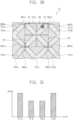
- FIG. 5B is an enlarged view of region CC illustrated in FIG. 5A .
- FIG. 5C is a graph illustrating a change in a detected signal according to input signals illustrated in FIG. 5B .
- the touch sensing unit TS includes a plurality of first touch sensors, a plurality of second touch sensors, a plurality of signal lines W11, W12, W13, W21, W22 and W23, and a plurality of pads PD.
- the first and second touch sensors are disposed in an active region AA.
- Each of the first touch sensors is arranged successively along a first direction DR1, and may have a shape extending in a second direction DR2.
- Each of the first touch sensors may include a plurality of first sensor parts TE1 and a plurality of fist connecting parts BR1 connecting the first sensor parts TE1.
- n number of the first touch sensors are provided and arranged successively along the first direction DR1.
- n is a natural number.
- the n first touch sensors are described as the first touch sensors.
- a first first touch sensor and nth first touch sensor may be disposed closest to a peripheral region NAA. As illustrated in FIG. 5A , the first first touch sensor and the nth first touch sensor are disposed closest to the peripheral region NAA while facing each other in the first direction DR1.
- the first sensor parts included in the first first touch sensor and the nth first touch sensor may have shapes different from those of the first sensor parts included in the second first touch sensor to the (n-1)th first touch sensor.
- the first sensor parts included in the first first touch sensor and the nth first touch sensor may have the same shapes as some of the first sensor parts included in the second first touch sensor to the (n-1)th first touch sensor.
- first touch sensor parts BR1 included in the first first touch sensor and the nth first touch sensor may be spaced apart from each other in the first direction DR1 and disposed on edges of the active region AA.
- Each of the second touch sensors is insulated from the first touch sensors and extends in the first direction DR1, and may have a shape arranged in the second direction DR2.
- Each of the second touch sensors may include a plurality of second sensor parts TE2 and a plurality of second connecting parts BR2 connecting the second sensor parts TE2.
- m number of the second touch sensors are provided and arranged in the second direction DR2.
- m is a natural number.
- the m second touch sensors are described as the second touch sensors.
- a first second touch sensor and mth second touch sensor among the m number of second touch sensors may be disposed closest to the peripheral region NAA.
- the first second touch sensor and the mth second touch sensor are disposed closest to the peripheral region NAA while facing each other in the second direction DR2.
- the second sensor parts included in the first second touch sensor and the mth second touch sensor may have shapes different from those of the second sensor parts included in the second second touch sensor to the (m-1)th second touch sensor.
- the second sensor parts included in the first second touch sensor and the mth second touch sensor may have the same shapes as some portions of the second sensor parts included in the second second touch sensor to the (m-1)th second touch sensor.
- the second touch sensor parts BR2 included in the first second touch sensor and the mth second touch sensor may be spaced apart from each other in the second direction DR2 and disposed on edges of the active region AA.
- the touch sensing unit TS may be differently operated according to whether a touch pen PN (see FIG. 4 ) operates or not.
- the touch sensing unit TS calculates a first electrostatic capacitance between the first touch sensors and the touch pen PN, and a second electrostatic capacitance between the second touch sensors and the touch pen PN.
- the touch sensing unit TS may detect a touch coordinate through the first and second electrostatic capacitances. This will be described in further detail with reference to FIG. 5B .
- the touch sensing unit TS may be operated through an electrostatic capacitive method in which the touch coordinate is detected through the electrostatic capacitance between the first touch sensors and the second touch sensors.
- the first sensor parts TE1 may output sensing signals, and the plurality of second sensor parts TE2 may receive driving signals.
- the touch sensing unit TS may scan the active region AA by applying driving signals to the second sensor parts TE2, and may detect a region on which a touch is applied through the sensing signals output from the plurality of first sensor parts TE1.
- the first sensor parts TE1 may also receive driving signals
- the second sensor parts TE2 may also output sensing signals and may further receive or output other electrical signals.
- the touch sensing unit TS may detect an external touch through various other methods such as a resistive film method, an optical method, an ultrasonic method, a coordinate recognition method, or the like, and may have a corresponding electrode structure.
- a plurality of signal lines and a plurality of pads PD may be disposed in the peripheral region NAA.
- a portion of the first signal lines W11, W12 and W13 and a portion of the second signal lines W21, W22 andW23 are illustrated. Ends of the first signal lines W11, W12 and W13 are respectively connected to the second touch sensors, and opposing ends of the second signal lines W21, W22 and W23 are respectively connected to the first touch sensors.
- Signal lines (not shown) from among the plurality of signal lines may be respectively connected to the corresponding electrodes from among the first and second touch sensors.
- a pad region PA may be defined in a portion of the peripheral region NAA.
- the pads PD are disposed in the pad region PA.
- the touch sensing unit TS may be connected to a power supply (not shown) and a driving circuit (not shown) through the pads PD.
- the pads PD include a plurality of first pads PD11, PD12 and PD13 and a plurality of second pads PD21, PD22 and PD23. For convenience in description, some pads are not illustrated.
- Ends of the first signal lines W11, W12 and W13 are respectively connected to the first pads PD11, PD12 and PD13.
- ends of the second signal lines W21, W22 and W23 are respectively connected to the second pads PD21, PD22 and PD23.
- FIGS. 5B and 5C a touch coordinate detection method of a touch sensing unit TS when a touch pen PN is used will be described.
- first sensor parts TE1a and first connecting parts BR1a included in the first first touch sensor, and first sensor parts TE1b and first connecting parts BR1b included in the second first touch sensor are illustrated.
- second sensor parts TE2a and second connecting parts BR2a included in the first second touch sensor, and second sensor parts TE2b and second connecting parts BR2b included in the second second touch sensor are illustrated.
- the same detection signals may be provided to the first and second touch sensors.
- the detection signals may be ground voltage.
- the embodiment of the inventive concept is not limited thereto, and the detection signal may be set so as to have a voltage level different from a voltage level provided to the detecting part DT of the touch pen PN.
- the voltage level provided to the detecting part DT is described as being greater than that of the detection signal.
- the touch sensing unit TS may detect the amount of change in voltage/current of the detection signal provided to the first and second touch sensors. As such, the touch sensing unit TS may recognize a touch coordinate on the basis of the amount of change in voltage/current of the detection signal provided to the first and second touch sensors.
- the voltage level of the detecting signal detected from the first sensor parts TE1a and TE1b may be changed.
- the electrostatic capacitance between the detecting part DT and the first sensor parts TE1a may be greater than that between the detecting part DT and the first sensor parts TE1b.
- the touch sensing unit TS may determine that the touch coordinate Po approaches closer to the first first sensor parts TE1a than to the second first sensor parts TE1b.
- the electrostatic capacitance between the detecting part DT and the second sensor parts TE2b may be greater than that between the detecting part DT and the second sensor parts TE2a.
- the touch sensing unit TS may determine that the touch coordinate Po approaches closer to the first second sensor parts TE2a than to the second second sensor parts TE2b.
- the touch sensing unit TS may determine that the touch coordinate Po is recognized in a second region B2 from among first to fourth regions B1 to B4.
- the connecting parts BR1 and BR2, and the sensor parts TE1 and TE2 connected through the connecting parts BR1 and BR2 may be disposed on the vicinity of the edges of the active region AA. Consequently, the touch sensing unit TS may readily detect the touch coordinate even when the vicinity of the edges of the active region AA is touched by the touch pen PN.
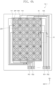
- FIG. 6A is a plan view of a touch sensing unit according to another embodiment of the inventive concept.
- FIG. 6B is an enlarged view of region XX illustrated in FIG. 6A .
- a touch sensing unit TS-1 illustrated in FIG. 6A may be only different in the configuration of its blocking electrode SPP, signal lines, and pads PD, but the remaining configuration may be substantially the same. Accordingly, descriptions of the remaining configuration will not be provided.
- the touch sensing unit TS-1 may include a blocking electrode SPP which prevents the occurrence of coupling between the first touch sensors and the signal lines or between the second touch sensors and the signal lines.
- the blocking electrode SPP may include a conductive material.
- the blocking electrode SPP may include any one of indium tin oxide (ITO), indium zinc oxide (IZO), zinc oxide (ZnO), indium tin zinc oxide (ITZO), PEDOT, or a metal.
- the metal may include molybdenum, silver, titanium, copper, aluminum, and alloys thereof.
- the blocking electrode SPP may be disposed in a peripheral region NAA adjacent to an active region AA. According to an embodiment, the blocking electrode SPP may be disposed in a peripheral region NAA to surround the active region AA. However, the embodiment of the inventive concept is not limited thereto, and the blocking electrode SPP may be disposed in the peripheral region NAA adjacent to the active region AA through various methods. For example, the blocking electrode SPP may be disposed in the peripheral region NAA adjacent to ends of the signal lines connected to sensor parts TE1 and TE2.
- the touch sensing unit TS-1 may include first to fourth signal lines. That is, the first to fourth signal lines may be respectively connected to two ends of each of the first and second touch sensors. Detection signals may be respectively provided to two ends of each of the first and second touch sensors through the first to fourth signal lines. As a result, a uniform detection signal may be provided to the first sensor parts TE1 of the first touch sensors and the second sensor parts TE2 of the second touch sensors.
- each first signal line is connected to a first pad part PD1 and the other end of each first signal line is connected to a first touch sensor.
- One end of each second signal line is connected to a second pad part PD2 and the other end of each second signal line is connected to one of the first touch sensors.
- each third signal lines is connected to a third pad part PD3 and the other end of each third signal line is connected to one of the second touch sensors.
- One end of each fourth signal line is connected to a fourth pad part PD4 and the other end of each fourth signal line is connected to one of the second touch sensors. For convenience in description, some pads are not illustrated.
- the blocking electrode SPP may be disposed in the peripheral region NAA to surround the active region AA.
- the blocking electrode SPP blocks the occurrence of coupling between the first to fourth signal lines and the first touch sensors, or between the first to fourth signal lines and the second touch sensors.
- first to third signal lines Wa, Wb and Wc which are connected to the fourth pad part PD4 are exemplarily illustrated.
- a detection signal is provided to the first to third signal lines Wa, Wb and Wc through the fourth pad parts PD4, coupling may occur between the first to third signal lines Wa, Wb and Wc and the sensor parts TE1 and TE2.
- the blocking electrode SPP is disposed in the peripheral region NAA adjacent to the active region AA. That is, the blocking electrode SPP may be disposed in the peripheral region NAA adjacent to the first to third signal lines Wa, Wb and Wc.
- a first coupling CS1 is formed between the first signal line Wa and the blocking electrode SPP.
- a second coupling CS2 is formed between the second signal line Wb and the blocking electrode SPP.
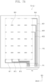
- FIG. 7A is a plan view illustrating a first conductive layer of the touch sensing unit illustrated in FIG. 6A .
- FIG. 7B is a plan view illustrating a second conductive layer of the touch sensing unit illustrated in FIG. 6A .
- FIG. 7C is a cross-sectional view showing the first and second conductive layers of the touch sensing unit according to another embodiment of the inventive concept.
- FIG. 8A is a cross-sectional view taken along line I-I' of FIG. 6A according to an embodiment of the inventive concept.
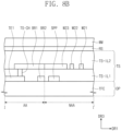
- FIG. 8B is a cross-sectional view taken along line I-I' of FIG. 6A according to another embodiment of the inventive concept.
- FIG. 8C is a cross-sectional view taken along line II-II' of FIG.
- FIG. 6A describes that the first conductive layer TS-CL1 includes first to fourth signal lines connected to the first to fourth pad regions PD1 to PD4.
- FIG. 7A describes that the first conductive layer TS-CL1 includes the third and fourth signal lines connected to the third and fourth pad regions PD3 and PD4 shown in FIG. 6A . That is, the first and second signal lines connected to the first and second pad regions PD1 to PD2 may be omitted.
- the touch sensing unit TS may include the first conductive layer TS-CL1 and the second conductive layer TS-CL2.
- the touch sensing unit TS may be directly disposed on the display panel DP. That is, the first conductive layer TS-CL1 is disposed directly on the encapsulating substrate TFE.
- the first insulating layer TS-IL1 may be disposed on the first conductive layer TS-CL1, and the second conductive layer TS-CL2 may be disposed on the first insulating layer TS-IL1.
- first conductive layer TS-CL1 may include first connecting parts BR1 of first touch sensors, signal lines W11 to W13 and W21 to W23, and pads PD. That is, the first connecting parts BR1, the signal lines W11 to W13 and W21 to W23, and the pads PD may be disposed on an encapsulating substrate TFE. As illustrated in FIG. 8A , pads PD are not provided, and only a portion of signal lines from among the signal lines W11 to W13 and W21 to W23 is disclosed for simplicity in explanation.
- a first insulating layer TS-IL1 may be disposed on the first conductive layer TS-CL1 so as to cover the first connecting parts BR1, the signal lines W11 to W13 and W21 to W23, and the pads PD.
- touch contact holes TS-CH which expose at least a portion of first sensor parts TE1 may be defined in the first insulating layer TS-IL1.
- the first connecting parts BR1 are connected to the first sensor parts TE1 through the touch contact holes TS-CH.
- the first connecting parts BR1 may be directly connected to the signal lines W21 to W23 respectively and provide an electrical signal to the first sensor parts TE1.
- a second conductive layer TS-CL2 may include first sensor parts TE1, second sensor parts TE2, second connecting parts BR2, and a blocking electrode SPP. That is, the first sensor parts TE1, the second sensor parts TE2 of the second touch sensors, the second connecting parts BR2, and the blocking electrode SPP are disposed on the first insulating layer TS-IL1.
- the first sensor parts TE1, the second sensor parts TE2 and the second connecting parts BR2 are disposed on a layer different from that on which the fist connecting parts BR1 and the signal lines W11 to W13 and W21 to W23 are disposed.
- a second insulating layer TS-IL2 may be disposed on the second conductive layer TS-CL2 so as to cover the first sensor parts TE1, second sensor parts TE2, second connecting parts BR2, and the blocking electrode SPP.
- a window member WM may be disposed on the second insulating layer TS-IL2.
- An adhesive layer RS may be disposed between the second insulating layer TS-IL2 and the window member WM.
- the adhesive layer RS may be a resin.
- FIG. 8B cross-sectional views of a touch sensing unit TS according to another embodiment of the inventive concept are illustrated.
- the touch sensing unit TS shown in FIG. 8B is different from the touch sensing unit shown in FIG. 8A in that the first sensor parts TE1, the second sensor parts TE2, and the second connecting parts BR2 are disposed on the encapsulating substrate TFE.
- the first connecting parts BR1 and the signal lines W11 to W13 and W21 to W23 are disposed on the first insulating layer TS-IL1.
- a first conductive layer TS-CL1 may include first sensor parts TE1, second sensor parts TE2, second connecting parts BR2, and a blocking electrode SPP. That is, the first sensor parts TE1, the second sensor parts TE2, the second connecting parts BR2, and the blocking electrode SPP are disposed on the encapsulating substrate TFE.
- a second conductive layer TS-CL2 may include first connecting parts BR1, signal lines W11 to W13 and W21 to W23, and pads PD. That is, the first connecting parts BR1, the signal lines W11 to W13 and W21 to W23, and the pads PD may be disposed on a first insulating layer TS-IL1.
- the blocking electrode SPP may be disposed on a layer different from that on which the signal lines are disposed, and may prevent the occurrence of coupling between the signal lines and the sensor parts.
- the touch sensing unit TS shown in FIG. 7C is different from the touch sensing unit shown in FIGS. 7A and 7B in that the first sensor parts TE1, the second sensor parts TE2, the second connecting parts BR2, and the blocking electrode SPP are disposed on the encapsulating substrate TFE. Also, the first connecting parts BR1 and the first to third signal wirings W21, W22 and W23 are disposed on the first insulation layer TS-IL1. The first connecting parts BR1 connect the first sensor parts TE1 through the touch contact holes TS-CH. The first to third signal lines W21, W22 and W23 are also connected to the first sensor parts TE1 through the contact holes defined in the first insulating layer TS-IL1.
- signal lines W11 to W13 and W21 to W23 may be directly connected to second connecting parts BR2.
- a wiring contact hole W-CH for connecting the signal lines W11 to W13 and W21 to W23 and the second connecting parts BR2 may be defined in a first insulating layer TS-IL1.
- connection parts connecting the sensor parts may be disposed adjacent to a peripheral region.
- reliability of touch detection may be improved in the vicinity of an edge in the active region.
Landscapes
- Engineering & Computer Science (AREA)
- General Engineering & Computer Science (AREA)
- Theoretical Computer Science (AREA)
- Human Computer Interaction (AREA)
- Physics & Mathematics (AREA)
- General Physics & Mathematics (AREA)
- Devices For Indicating Variable Information By Combining Individual Elements (AREA)
- Electroluminescent Light Sources (AREA)
- Position Input By Displaying (AREA)
Applications Claiming Priority (2)
| Application Number | Priority Date | Filing Date | Title |
|---|---|---|---|
| KR1020160089409A KR102599283B1 (ko) | 2016-07-14 | 2016-07-14 | 표시장치 및 이를 포함하는 휴대용 단말기 |
| EP17181506.1A EP3270270A3 (de) | 2016-07-14 | 2017-07-14 | Anzeigevorrichtung mit integrierten berührungssensoren und tragbares endgerät damit |
Related Parent Applications (1)
| Application Number | Title | Priority Date | Filing Date |
|---|---|---|---|
| EP17181506.1A Division EP3270270A3 (de) | 2016-07-14 | 2017-07-14 | Anzeigevorrichtung mit integrierten berührungssensoren und tragbares endgerät damit |
Publications (2)
| Publication Number | Publication Date |
|---|---|
| EP4332740A2 true EP4332740A2 (de) | 2024-03-06 |
| EP4332740A3 EP4332740A3 (de) | 2024-05-29 |
Family
ID=59350802
Family Applications (2)
| Application Number | Title | Priority Date | Filing Date |
|---|---|---|---|
| EP24150051.1A Pending EP4332740A3 (de) | 2016-07-14 | 2017-07-14 | Anzeigevorrichtung und tragbares endgerät damit |
| EP17181506.1A Ceased EP3270270A3 (de) | 2016-07-14 | 2017-07-14 | Anzeigevorrichtung mit integrierten berührungssensoren und tragbares endgerät damit |
Family Applications After (1)
| Application Number | Title | Priority Date | Filing Date |
|---|---|---|---|
| EP17181506.1A Ceased EP3270270A3 (de) | 2016-07-14 | 2017-07-14 | Anzeigevorrichtung mit integrierten berührungssensoren und tragbares endgerät damit |
Country Status (4)
| Country | Link |
|---|---|
| US (5) | US10928939B2 (de) |
| EP (2) | EP4332740A3 (de) |
| KR (1) | KR102599283B1 (de) |
| CN (1) | CN107621901B (de) |
Families Citing this family (10)
| Publication number | Priority date | Publication date | Assignee | Title |
|---|---|---|---|---|
| CN105244365B (zh) * | 2015-11-18 | 2018-09-25 | 上海天马有机发光显示技术有限公司 | 显示装置、制造方法及显示设备 |
| KR102424289B1 (ko) * | 2017-06-01 | 2022-07-25 | 엘지디스플레이 주식회사 | 터치표시장치 및 터치패널 |
| KR102414940B1 (ko) | 2017-10-31 | 2022-06-29 | 엘지디스플레이 주식회사 | 표시 장치 및 그의 제조방법 |
| KR102503745B1 (ko) * | 2017-12-14 | 2023-02-23 | 엘지디스플레이 주식회사 | 전계발광 표시장치 |
| KR102579896B1 (ko) * | 2018-09-03 | 2023-09-20 | 삼성디스플레이 주식회사 | 표시 장치 및 이의 구동 방법 |
| KR102708639B1 (ko) * | 2019-07-22 | 2024-09-23 | 삼성디스플레이 주식회사 | 펜 감지 유닛 및 이를 포함하는 표시 장치 |
| KR102918073B1 (ko) * | 2020-02-27 | 2026-01-27 | 삼성디스플레이 주식회사 | 표시 장치 |
| KR102899032B1 (ko) | 2020-04-13 | 2025-12-12 | 삼성디스플레이 주식회사 | 표시 장치 |
| KR20230020061A (ko) | 2021-08-02 | 2023-02-10 | 삼성디스플레이 주식회사 | 전자 장치 |
| KR20230098391A (ko) | 2021-12-24 | 2023-07-04 | 삼성디스플레이 주식회사 | 표시 장치 |
Family Cites Families (39)
| Publication number | Priority date | Publication date | Assignee | Title |
|---|---|---|---|---|
| US6215476B1 (en) * | 1997-10-10 | 2001-04-10 | Apple Computer, Inc. | Flat panel display with integrated electromagnetic pen digitizer |
| JP2009251592A (ja) * | 2008-04-03 | 2009-10-29 | Samsung Mobile Display Co Ltd | 有機電界発光表示装置 |
| JP5113773B2 (ja) * | 2009-01-20 | 2013-01-09 | 株式会社ジャパンディスプレイイースト | 表示装置 |
| JP5439114B2 (ja) * | 2009-10-21 | 2014-03-12 | 株式会社ジャパンディスプレイ | 静電容量型入力装置および入力装置付き電気光学装置 |
| KR101726623B1 (ko) | 2010-03-16 | 2017-04-14 | 엘지디스플레이 주식회사 | 터치 패널 |
| KR20120027693A (ko) | 2010-09-13 | 2012-03-22 | 삼성전기주식회사 | 정전용량식 터치스크린 및 그 제조방법 |
| KR101886801B1 (ko) * | 2010-09-14 | 2018-08-10 | 삼성디스플레이 주식회사 | 터치 스크린 패널 일체형 평판표시장치 |
| TWI403795B (zh) | 2010-11-11 | 2013-08-01 | Wintek Corp | 觸控顯示裝置 |
| TWI443569B (zh) * | 2011-02-23 | 2014-07-01 | Wintek Corp | 電容式觸控面板 |
| KR101819677B1 (ko) | 2011-04-01 | 2018-01-17 | 엘지디스플레이 주식회사 | 터치 센서 일체형 표시장치 |
| KR101493556B1 (ko) | 2011-10-27 | 2015-02-16 | 엘지디스플레이 주식회사 | 터치 센서 내장형 유기발광 다이오드 표시장치 |
| KR101403482B1 (ko) | 2012-05-07 | 2014-06-05 | 한국화학연구원 | 벤조포르피린 유도체의 신규한 제조방법 및 이를 이용한 유기박막트랜지스터의 제조 |
| KR101542043B1 (ko) * | 2012-06-27 | 2015-08-06 | 엘지디스플레이 주식회사 | 터치 스크린 패널 |
| KR101694976B1 (ko) | 2012-08-21 | 2017-01-10 | 한국전자통신연구원 | Dmb 시스템에서 제한수신 메시지 전송 방법 및 그 장치 |
| KR20140077392A (ko) | 2012-12-14 | 2014-06-24 | 현대중공업 주식회사 | 해상풍력 하부구조물 고정용 파일 시공구조 |
| KR102107576B1 (ko) | 2012-12-21 | 2020-05-07 | 엘지디스플레이 주식회사 | 터치패널 및 이를 이용한 표시장치 |
| KR20140087695A (ko) * | 2012-12-31 | 2014-07-09 | 삼성디스플레이 주식회사 | 감지부를 포함하는 표시 장치 및 그 구동 방법 |
| CN103257769B (zh) | 2013-03-25 | 2016-01-27 | 合肥京东方光电科技有限公司 | 一种电容内嵌式触摸屏和显示装置 |
| KR101508421B1 (ko) | 2013-04-02 | 2015-04-07 | 부산대학교 산학협력단 | 생분해성 포스포아미드 링커에 의해 가교된 peg 하이드로젤 및 이의 제조 방법 |
| KR20140121185A (ko) | 2013-04-05 | 2014-10-15 | 연세대학교 산학협력단 | 전자 공력 제트 프린팅 기법을 이용한 cnt필터 제작 시스템 및 cnt필터 제작 방법, 이 제작 방법에 의해 제작된 cnt필터 |
| KR101478043B1 (ko) | 2013-04-24 | 2015-01-02 | 일진디스플레이(주) | 터치 패널 및 그 제조 방법 |
| KR102096622B1 (ko) * | 2013-08-19 | 2020-04-03 | 삼성디스플레이 주식회사 | 유기발광 표시장치 |
| KR102081318B1 (ko) * | 2013-09-23 | 2020-04-14 | 엘지디스플레이 주식회사 | 터치센서 내장형 액정 표시장치 |
| TW201516765A (zh) * | 2013-10-16 | 2015-05-01 | Elan Microelectronics Corp | 可判斷功能切換的觸控裝置、系統及其功能切換控制方法 |
| KR20150045288A (ko) | 2013-10-18 | 2015-04-28 | 삼성디스플레이 주식회사 | 터치 패널 |
| KR102192035B1 (ko) * | 2013-12-02 | 2020-12-17 | 삼성디스플레이 주식회사 | 접촉 감지 센서를 포함하는 플렉서블 표시 장치 |
| CN103926728B (zh) * | 2013-12-30 | 2016-11-16 | 上海天马微电子有限公司 | 一种集成触控功能的液晶显示装置 |
| KR20140041624A (ko) | 2014-01-20 | 2014-04-04 | 김영광 | 에어 튜브를 이용한 슬로싱 저감장치 및 그 방법 |
| KR20150103552A (ko) | 2014-03-03 | 2015-09-11 | 삼성전자주식회사 | 디스플레이 장치 및 이의 제조방법 |
| KR102381284B1 (ko) | 2014-04-08 | 2022-03-31 | 삼성디스플레이 주식회사 | 터치 센서를 포함하는 터치 패널 |
| KR102175649B1 (ko) | 2014-06-24 | 2020-11-06 | 엘지이노텍 주식회사 | 터치윈도우 |
| KR20160025440A (ko) * | 2014-08-27 | 2016-03-08 | 삼성전자주식회사 | 터치 패널 및 이를 구비한 좌표 측정 시스템 |
| KR102259239B1 (ko) | 2014-09-11 | 2021-06-01 | 엘지디스플레이 주식회사 | 터치패널이 구비된 표시장치 |
| KR102230549B1 (ko) | 2014-09-12 | 2021-03-22 | 삼성디스플레이 주식회사 | 접촉 감지 기능을 가진 광학계 및 이를 포함하는 표시 장치 |
| KR102252543B1 (ko) | 2014-09-12 | 2021-05-17 | 엘지이노텍 주식회사 | 터치 디바이스, 터치 펜 및 터치 패널 |
| KR102221910B1 (ko) | 2014-10-10 | 2021-03-05 | 삼성디스플레이 주식회사 | 표시장치 및 그 제조방법 |
| KR102250847B1 (ko) | 2014-11-13 | 2021-05-13 | 삼성디스플레이 주식회사 | 터치 스크린 패널 일체형 표시장치 |
| KR102264760B1 (ko) * | 2014-11-26 | 2021-06-14 | 삼성디스플레이 주식회사 | 터치 센서를 포함하는 표시 장치 및 그 제조 방법 |
| KR102481057B1 (ko) * | 2015-12-30 | 2022-12-27 | 엘지디스플레이 주식회사 | 터치 일체형 표시패널 및 그를 포함하는 표시장치 |
-
2016
- 2016-07-14 KR KR1020160089409A patent/KR102599283B1/ko active Active
-
2017
- 2017-07-03 US US15/641,023 patent/US10928939B2/en active Active
- 2017-07-14 CN CN201710573065.9A patent/CN107621901B/zh active Active
- 2017-07-14 EP EP24150051.1A patent/EP4332740A3/de active Pending
- 2017-07-14 EP EP17181506.1A patent/EP3270270A3/de not_active Ceased
-
2021
- 2021-02-22 US US17/180,902 patent/US11416092B2/en active Active
-
2022
- 2022-07-07 US US17/859,775 patent/US11669185B2/en active Active
-
2023
- 2023-04-26 US US18/139,400 patent/US12045408B2/en active Active
-
2024
- 2024-06-28 US US18/757,546 patent/US12524094B2/en active Active
Also Published As
| Publication number | Publication date |
|---|---|
| US20230266836A1 (en) | 2023-08-24 |
| EP4332740A3 (de) | 2024-05-29 |
| EP3270270A3 (de) | 2018-04-25 |
| US20180018053A1 (en) | 2018-01-18 |
| US11669185B2 (en) | 2023-06-06 |
| US20220342501A1 (en) | 2022-10-27 |
| US11416092B2 (en) | 2022-08-16 |
| KR20180008968A (ko) | 2018-01-25 |
| EP3270270A2 (de) | 2018-01-17 |
| CN107621901B (zh) | 2023-07-07 |
| KR102599283B1 (ko) | 2023-11-08 |
| US12045408B2 (en) | 2024-07-23 |
| US20210173507A1 (en) | 2021-06-10 |
| US10928939B2 (en) | 2021-02-23 |
| US20240353942A1 (en) | 2024-10-24 |
| US12524094B2 (en) | 2026-01-13 |
| CN107621901A (zh) | 2018-01-23 |
Similar Documents
| Publication | Publication Date | Title |
|---|---|---|
| US12045408B2 (en) | Display device and portable terminal including same | |
| US20260007034A1 (en) | Organic light emitting display module and organic light emitting display device having the same | |
| KR102795318B1 (ko) | 표시 장치 | |
| KR102765362B1 (ko) | 감지 유닛 및 이를 포함하는 표시 장치 | |
| KR102458892B1 (ko) | 플렉서블 표시장치 및 그의 제조방법 | |
| EP3258358B1 (de) | Integriertes berührungsempfindliches anzeigegerät mit einem einschichtigen kapazitiven touch-panel | |
| CN103972260B (zh) | 集成有触摸屏面板的有机发光显示器 | |
| KR102350084B1 (ko) | 터치 패널 및 이를 이용한 표시장치 | |
| CN112534384B (zh) | 带检测装置的显示设备 | |
| KR20160017336A (ko) | 인 셀 타입의 터치 구조를 갖는 유기발광표시장치 | |
| CN111724740B (zh) | 显示面板和显示装置 | |
| KR20180119196A (ko) | 표시모듈 | |
| TW202001527A (zh) | 觸控感測器及其顯示裝置 | |
| KR102594615B1 (ko) | 입력감지유닛 및 이를 포함하는 표시장치 | |
| KR102829293B1 (ko) | 표시모듈 및 이를 포함하는 표시장치 | |
| US20190243485A1 (en) | Touch input device | |
| KR20140110446A (ko) | 터치스크린패널 일체형 표시장치 | |
| JP2012003768A (ja) | タッチ式透明キーボード | |
| US20160034096A1 (en) | Flat self-luminous touch switch | |
| US20250120272A1 (en) | Display device | |
| TWM515153U (zh) | 觸控顯示面板 | |
| TWI575433B (zh) | 觸控顯示面板 | |
| KR102798043B1 (ko) | 표시 장치 | |
| KR20170062604A (ko) | 터치 스크린 패널, 및 이를 포함하는 표시장치 |
Legal Events
| Date | Code | Title | Description |
|---|---|---|---|
| PUAI | Public reference made under article 153(3) epc to a published international application that has entered the european phase |
Free format text: ORIGINAL CODE: 0009012 |
|
| STAA | Information on the status of an ep patent application or granted ep patent |
Free format text: STATUS: THE APPLICATION HAS BEEN PUBLISHED |
|
| AC | Divisional application: reference to earlier application |
Ref document number: 3270270 Country of ref document: EP Kind code of ref document: P |
|
| AK | Designated contracting states |
Kind code of ref document: A2 Designated state(s): AL AT BE BG CH CY CZ DE DK EE ES FI FR GB GR HR HU IE IS IT LI LT LU LV MC MK MT NL NO PL PT RO RS SE SI SK SM TR |
|
| REG | Reference to a national code |
Ref country code: DE Ref legal event code: R079 Free format text: PREVIOUS MAIN CLASS: G06F0003044000 Ipc: G06F0003041000 |
|
| PUAL | Search report despatched |
Free format text: ORIGINAL CODE: 0009013 |
|
| AK | Designated contracting states |
Kind code of ref document: A3 Designated state(s): AL AT BE BG CH CY CZ DE DK EE ES FI FR GB GR HR HU IE IS IT LI LT LU LV MC MK MT NL NO PL PT RO RS SE SI SK SM TR |
|
| RIC1 | Information provided on ipc code assigned before grant |
Ipc: G06F 3/044 20060101ALI20240424BHEP Ipc: G06F 3/041 20060101AFI20240424BHEP |
|
| STAA | Information on the status of an ep patent application or granted ep patent |
Free format text: STATUS: REQUEST FOR EXAMINATION WAS MADE |
|
| 17P | Request for examination filed |
Effective date: 20241125 |
|
| RBV | Designated contracting states (corrected) |
Designated state(s): AL AT BE BG CH CY CZ DE DK EE ES FI FR GB GR HR HU IE IS IT LI LT LU LV MC MK MT NL NO PL PT RO RS SE SI SK SM TR |
|
| P01 | Opt-out of the competence of the unified patent court (upc) registered |
Free format text: CASE NUMBER: UPC_APP_0006919_4332740/2026 Effective date: 20260226 |