EP4332809A1 - End-to-end-transaktionsintegrität durch standardverbindung - Google Patents
End-to-end-transaktionsintegrität durch standardverbindung Download PDFInfo
- Publication number
- EP4332809A1 EP4332809A1 EP22306293.6A EP22306293A EP4332809A1 EP 4332809 A1 EP4332809 A1 EP 4332809A1 EP 22306293 A EP22306293 A EP 22306293A EP 4332809 A1 EP4332809 A1 EP 4332809A1
- Authority
- EP
- European Patent Office
- Prior art keywords
- integrity
- transaction
- regular
- subsystem
- soc
- Prior art date
- Legal status (The legal status is an assumption and is not a legal conclusion. Google has not performed a legal analysis and makes no representation as to the accuracy of the status listed.)
- Granted
Links
Images


Classifications
-
- G—PHYSICS
- G06—COMPUTING OR CALCULATING; COUNTING
- G06F—ELECTRIC DIGITAL DATA PROCESSING
- G06F21/00—Security arrangements for protecting computers, components thereof, programs or data against unauthorised activity
- G06F21/60—Protecting data
- G06F21/64—Protecting data integrity, e.g. using checksums, certificates or signatures
-
- H—ELECTRICITY
- H04—ELECTRIC COMMUNICATION TECHNIQUE
- H04L—TRANSMISSION OF DIGITAL INFORMATION, e.g. TELEGRAPHIC COMMUNICATION
- H04L63/00—Network architectures or network communication protocols for network security
- H04L63/12—Applying verification of the received information
- H04L63/123—Applying verification of the received information received data contents, e.g. message integrity
-
- H—ELECTRICITY
- H04—ELECTRIC COMMUNICATION TECHNIQUE
- H04L—TRANSMISSION OF DIGITAL INFORMATION, e.g. TELEGRAPHIC COMMUNICATION
- H04L1/00—Arrangements for detecting or preventing errors in the information received
- H04L1/004—Arrangements for detecting or preventing errors in the information received by using forward error control
-
- G—PHYSICS
- G06—COMPUTING OR CALCULATING; COUNTING
- G06F—ELECTRIC DIGITAL DATA PROCESSING
- G06F11/00—Error detection; Error correction; Monitoring
- G06F11/07—Responding to the occurrence of a fault, e.g. fault tolerance
- G06F11/08—Error detection or correction by redundancy in data representation, e.g. by using checking codes
-
- G—PHYSICS
- G06—COMPUTING OR CALCULATING; COUNTING
- G06F—ELECTRIC DIGITAL DATA PROCESSING
- G06F11/00—Error detection; Error correction; Monitoring
- G06F11/07—Responding to the occurrence of a fault, e.g. fault tolerance
- G06F11/08—Error detection or correction by redundancy in data representation, e.g. by using checking codes
- G06F11/10—Adding special bits or symbols to the coded information, e.g. parity check, casting out 9's or 11's
- G06F11/1004—Adding special bits or symbols to the coded information, e.g. parity check, casting out 9's or 11's to protect a block of data words, e.g. CRC or checksum
-
- G—PHYSICS
- G06—COMPUTING OR CALCULATING; COUNTING
- G06F—ELECTRIC DIGITAL DATA PROCESSING
- G06F11/00—Error detection; Error correction; Monitoring
- G06F11/07—Responding to the occurrence of a fault, e.g. fault tolerance
- G06F11/08—Error detection or correction by redundancy in data representation, e.g. by using checking codes
- G06F11/10—Adding special bits or symbols to the coded information, e.g. parity check, casting out 9's or 11's
- G06F11/1008—Adding special bits or symbols to the coded information, e.g. parity check, casting out 9's or 11's in individual solid state devices
- G06F11/1048—Adding special bits or symbols to the coded information, e.g. parity check, casting out 9's or 11's in individual solid state devices using arrangements adapted for a specific error detection or correction feature
-
- G—PHYSICS
- G06—COMPUTING OR CALCULATING; COUNTING
- G06F—ELECTRIC DIGITAL DATA PROCESSING
- G06F13/00—Interconnection of, or transfer of information or other signals between, memories, input/output devices or central processing units
- G06F13/38—Information transfer, e.g. on bus
- G06F13/40—Bus structure
- G06F13/4004—Coupling between buses
-
- G—PHYSICS
- G06—COMPUTING OR CALCULATING; COUNTING
- G06F—ELECTRIC DIGITAL DATA PROCESSING
- G06F15/00—Digital computers in general; Data processing equipment in general
- G06F15/76—Architectures of general purpose stored program computers
- G06F15/78—Architectures of general purpose stored program computers comprising a single central processing unit
- G06F15/7807—System on chip, i.e. computer system on a single chip; System in package, i.e. computer system on one or more chips in a single package
- G06F15/7825—Globally asynchronous, locally synchronous, e.g. network on chip
-
- G—PHYSICS
- G06—COMPUTING OR CALCULATING; COUNTING
- G06F—ELECTRIC DIGITAL DATA PROCESSING
- G06F21/00—Security arrangements for protecting computers, components thereof, programs or data against unauthorised activity
- G06F21/60—Protecting data
- G06F21/606—Protecting data by securing the transmission between two devices or processes
-
- H—ELECTRICITY
- H04—ELECTRIC COMMUNICATION TECHNIQUE
- H04L—TRANSMISSION OF DIGITAL INFORMATION, e.g. TELEGRAPHIC COMMUNICATION
- H04L9/00—Cryptographic mechanisms or cryptographic arrangements for secret or secure communications; Network security protocols
- H04L9/40—Network security protocols
Definitions
- the present invention is directed in general to the field of information handling systems.
- the present invention relates to providing data transaction integrity checking and recovery in a standard interconnect used with information handling systems.
- Information handling systems are computer-based instrumentalities primarily designed to compute, classify, process, transmit, receive, retrieve, originate, switch, store, display, manifest, measure, detect, record, reproduce, handle, or utilize any form of information, intelligence or data for business, scientific, control, or other purposes.
- information handling systems are implemented in integrated circuit form with any suitable configuration of one or more microprocessors or microcontrollers, but different integrated circuit configurations provide different challenges for implementing required information handling system functionality.
- a multiprocessor system on a chip is a single integrated circuit die, substrate, or microchip that includes a plurality of CPU processors or cores that communicate over an interconnect network or bus with a combination with additional components of a computer or other electronic system on a single integrated circuit die, substrate, or microchip.
- SoC system on a chip
- These data integrity challenges are amplified with SoC-based information handling systems which do not only rely on local embedded tightly coupled memories (TCMs), but instead execute code from external DRAM which presents a challenge with ensuring the integrity of the code/data exchanged with the CPU processor(s)/core(s).
- DRAM controllers often include in-line error correction coding (ECC) features to protect data integrity in the DRAM, the communication link between the CPU processor(s)/core(s) and DRAM controller remains susceptible to data errors or faults.
- NoC network-on-chip
- a transaction integrity protection system, apparatus, and method of operation are described for providing end-to-end transaction integrity of regular transactions sent over an interconnect by sending an extra protecting information transaction (PIT) message over the interconnect with each regular transaction to be protected.
- each PIT message includes integrity information (e.g., with cyclic redundancy check (CRC) data or other suitable error-detecting coding techniques) that can be processed to detect faults that may arise when the regular transaction is sent over the interconnect.
- CRC cyclic redundancy check
- the disclosed transaction integrity system may be implemented with a Transaction Checker Generator (TCG) hardware circuit and a Transaction Checker EndPoint (TCEP) hardware circuit that are posited on opposite ends of an interconnect path.
- the TCG hardware circuit sends the regular transaction and also generates the PIT message for transmission that will be used to protect the regular transaction over the interconnect path.
- the PIT message may be a small (e.g., 32-bits) message which is generated from the regular transaction being protected and includes a user bit and CRC value, along with a shared destination address and transaction ID.
- the TCG hardware circuit also checks responses to each regular transaction and PIT message to detect any fault that may have happened during transfer over the interconnect path.
- the TCEP hardware circuit may be connected and configured to receive the regular transaction and the PIT message and to evaluate the integrity of the regular transaction based on the PIT message, depending on the regular transaction type.
- the TCEP hardware circuit that receives a regular write transaction may compute protecting information (e.g., CRC data) based on received request information and write data in the regular write transaction, and then compare the computed CRC data to the CRC data received in the PIT message.
- the TCEP hardware circuit that receives a regular read transaction may compute protecting information (e.g., CRC data) based on received data for the regular read transaction, and then send the protecting information back to the originating TCG hardware circuit in the read data of the PIT message.
- the TCEP hardware circuit is also configured to generate and check parity information going along with regular transaction toward its final destination.
- TCEP hardware circuit located at each end point of an interconnect path that can be reached by a subsystem with a TCG hardware circuit.
- One category of fault which can occur is the loss or misdirection of an entire packet. This can be managed by both the TCEP and TCG having an expected sequence of packets based on a packet ID. Similar to corruptions detected by CRC errors, a loss (or misdirected packet) can be detected by seeing inconsistencies on the sequence, or by using a timeout when no suitable packet is received.
- the disclosed transaction integrity protection mechanism may be used with an arbitrary non-safety aware interconnect or similar network, whether embodied entirely on a SOC or between multiple SOC using a general network.
- a non-safety aware interconnect may be understood to refer to any suitable transport mechanism (interconnect/network) which lacks inbuilt mechanisms for error concealment/recovery or to fulfill functional safety requirements, including but not limited to a network-on-chip (NoC) bus which does not include built-in integrity protection structures. And by supporting both non-protected and protected transactions flowing through the interconnect path, there is no overhead required to support non-safety related initiators. As a result, the interconnect need not be modified to add safety capability to a subset of the traffic.
- the disclosed transaction integrity protection mechanism enables safety information to be conveyed using standard information packets which are routed independently of the functional packets and with no fixed timing relationship.
- an algorithm refers to a self-consistent sequence of steps leading to a desired result, where a "step” refers to a manipulation of physical quantities which may, though need not necessarily, take the form of electrical or magnetic signals capable of being stored, transferred, combined, compared, and otherwise manipulated. It is common usage to refer to these signals as bits, values, elements, symbols, characters, terms, numbers, or the like. These and similar terms may be associated with the appropriate physical quantities and are merely convenient labels applied to these quantities.
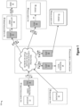
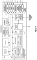
- FIG. 1 there is depicted schematic block diagram 100 of a system on a chip (SOC) including a plurality of SoC subsystems 10, 30, 40, 50, 60 connected together over an interconnect subsystem 20.
- SoC subsystems 10, 60 are transaction initiators which issue or send transactions over the interconnect subsystem 20 to one or more target SoC subsystems 30, 40, 50 which receive and process and process the transactions.
- the interconnect subsystem 20 is illustrated as being implemented with a network-on-chip (NoC) 21 which does not include built-in transaction integrity protection, it will be appreciated that any suitable interconnect or crossbar switch may be used (e.g., DMB/DBS/AXI/SSI).
- an initiator module 11 e.g., a Cortex-M4 CPU or other System Controller Unit (SCU)
- SCU System Controller Unit
- TCG Transaction Checker Generator
- each PIT message includes one or more user bit fields which are set to identify the transaction as a PIT message, and also includes the same destination address and transaction ID as the regular transaction being protected so that it is directed to the same target SoC subsystem as the regular transaction.
- each TCG (e.g., 12) is connected and configured to receive regular transaction responses (not shown) along with accompanying PIT response (PITR) messages which are returned over the interconnect subsystem 20 by the target SoC subsystem.
- PITR PIT response
- an initiator module 61 is connected and configured to send transactions directly over the interconnect subsystem 20.
- a Transaction Checker EndPoint is connected to receive and process transactions from the interconnect subsystem 20 and to communicate over a parity-protected path (e.g., AXI/SSI bus) to a target module.
- TCEP Transaction Checker EndPoint
- each TCEP is connected and configured to generate regular transaction responses (not shown) along with accompanying PIT response (PITR) messages which are returned over the interconnect subsystem 20 to the initiating SoC subsystem.
- the DRAM SoC subsystem 30 includes a TCEP 31 that is connected to receive and process memory access transactions from the interconnect subsystem 20 by communicating over the parity-protected path to the DRAM controller 32 (which communicates over an inline ECC path with the DRAM memory 33) and by generating regular transaction responses (not shown) along with accompanying PIT response (PITR) messages for return to the initiating SoC subsystem.
- the SoC subsystem 40 includes a TCEP 41 that is connected to receive and process transactions from the interconnect subsystem 20 and to communicate over the parity-protected path to the target module 42.
- a target module 51 may be directly connected to receive and process transactions from the interconnect subsystem 20.
- interconnect subsystem 20 may include a TCEP 23 that is connected to receive and process transactions from the NoC 21 and to communicate with the local peripheral module 24 at the interconnect subsystem 20.
- the interconnect subsystem 20 includes a TCEP 22 that is connected to receive and process transactions from the NoC 21 and to communicate to the target module 51.
- the TCG or TCEP may generate each PIT or PITR message to be formatted to look like a regular transaction, but to also include protecting information.
- the PIT message may include the same destination address as the regular transaction (aligned on 32-bits boundary) and the same transaction ID as the regular transaction.
- the PIT message may include one or more user bit fields set to a first value (e.g., 0b1) to identify the transaction as a PIT message or to a second value (e.g., 0b0) to identify the transaction as a regular transaction.
- the user bit field could be triplicated to be resistant to a bit flip.
- the generated PIT message may include protecting information that is computed by using the CRC-32 checksum algorithm from ITU-T V.42 protocol to detect data corruption in the protected regular transaction, though any suitable error detection/correction protocol may be used.
- the PITR messages may be formatted to include the same information as the regular transaction response messages, such as destination address, and may also include protecting information computed at the TCEP.
- the data integrity protection for regular transactions sent over the interconnect subsystem 20 may be implemented with a synchronous integrity mode or an asynchronous integrity mode.
- the TCG circuit With the synchronous integrity mode, the TCG circuit generates a response to a regular transaction issued by an initiator SoC subsystem only after the PIT response comes back to the TCG.
- the integrity protection mechanism imposes a latency requirement since initiating SoC subsystem sees a transaction duration that is long enough to allow the regular transaction and response to fully navigate over the interconnect subsystem 20.
- the TCG circuit With the asynchronous integrity mode, the TCG circuit generates an immediate response to a regular transaction issued by an initiator SoC subsystem, and if an error is detected when the PIT response comes back to the TCG, then the TCG generates an interrupt to signal there has been a PIT error.
- the protection mechanism provided in the asynchronous mode of protection has no impact on the latency seen by the initiator since the transaction response is provided more quickly. In case of an initiating processor core subsystem, this may result in the execution or consumption of corrupted code or data, but the issuance of an interrupt may be then used to delete the corrupted code/data operation.
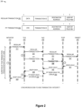
- FIG. 2 depicts a simplified diagrammatic illustration of the transactions handle by SoC subsystems 210, 250 which include TCG unit 220 and TCEP unit 240 to provide synchronous end-to-end integrity for communications over the NoC subsystem 230.
- the initiator subsystem 210 issues a regular transaction 211 which is sent to the TCG unit 220.
- the regular transaction 211 may be a memory access request, such as a memory write request or memory read request.
- the regular transaction may have any suitable message format.
- the depicted regular transaction 201 is shown as an n-bit message that includes a user bit field set to first value (e.g., 0), a destination address field, a transaction ID field, and a data field.
- the TCG unit 220 forwards the regular transaction 221 to the NoC subsystem 230.
- the TCG unit 220 generates and forwards a PIT transaction 222 to the NoC subsystem 230 shortly after forwarding the regular transaction 221.
- the PIT transaction may also have any suitable message format.
- the depicted PIT transaction 202 is shown as a 32-bit message that includes a user bit field set to second value (e.g., 1), a destination address field, a transaction ID field, and a CRC data field.
- second value e.g. 1
- the contents of the PIT transaction fields will depend on the type of regular transaction being protected.
- the TCG unit 220 may compute integrity information for a regular write transaction by using the write address and data fields to compute a CRC value, and then generating the 32-bit non-modifiable write carrying PIT transaction 222.
- the TCG unit 220 may start to compute integrity information for a regular read transaction by storing the read address of the regular transaction for subsequent retrieval, and then generating the 32-bit non-modifiable read PIT transaction 222.
- the regular transaction 221 and PIT transaction 222 are received and forwarded to the TCEP unit 240, respectively, as the regular transaction 231 and PIT transaction 232.
- the transactions 221, 222 are forwarded with little or no delay since there is no latency caused by complex transaction processing.
- the TCEP unit 240 responds to the regular transaction 231 by forwarding the regular transaction 241 to the target SoC subsystem 250.
- the TCEP unit 240 receives the forwarded PIT transaction 232 and then awaits receipt of the response message 251 from the target SoC subsystem 250 before computing the response message 242 and PIT response message 243.
- the TCEP unit 240 forwards it as the response message 242 to the NoC subsystem 230.
- the TCEP unit 240 computes a PIT response message 243.
- the response message 242 and PIT response message 243 may have any suitable message format and may include, for example, a user bit field, a destination address field, a transaction ID field, and a payload field. As disclosed herein, the contents of the PIT response message fields will depend on the type of regular transaction being protected.
- the TCEP unit 240 may compute the expected integrity protecting information for a regular write transaction by using the write address and data contained in the regular transaction 231 to compute local integrity information (e.g., local CRC values).
- local integrity information e.g., local CRC values
- the TCEP unit 240 may be configured to use only the write address from the first regular transaction 231 and to keep computing integrity information with data from additional regular transaction(s) 231 only as long as it receives regular transactions until a PIT transaction (e.g., 232) is received that corresponds to the regular transaction (e.g., 231).
- the TCEP 240 Upon receiving the PIT transaction 232, the TCEP 240 checks that the integrity information (e.g., CRC values) received with the PIT transaction 232 corresponds to the local integrity information, and also compares the write address from the PIT transaction 232 with the write address of the first regular transaction 231. If the received integrity information matches the local integrity information and if there is a match between the write addresses of the PIT transaction 232 and first regular transaction 231, the TCEP unit 240 generates the "OKAY" PIT response message 243, but if they do not match, then the TCEP unit 240 generates the "ERROR" PIT response message 243.
- the integrity information e.g., CRC values
- the TCEP unit 240 may compute the expected integrity information for a regular read transaction by beginning computation of local integrity information (e.g., local CRC values) using the read address of the regular transaction 231, and then updating the computation of the local integrity information with the read data returned in the read data response message 251 from the target SoC subsystem 250.
- the TCEP unit 240 may be configured to use only the read address from the first regular transaction 231.
- the TCEP unit 240 also forwards read data response message 251 to the NoC subsystem 230 as a forwarded response message 242 along with the PIT response message 243.
- the read data response message 251 to the regular transaction 241 is ERROR
- the integrity information is corrupted before being sent to the NoC subsystem 230, in which case the TCEP unit 240 generates the "ERROR” PIT response message 243. Otherwise, the TCEP unit 240 generates the "OKAY" PIT response message 243 which includes the local integrity information (e.g., local CRC values).
- the regular response message 242 and PIT response message 243 are received and forwarded to the TCG unit 220, respectively as the regular response message 233 and PIT response message 234.
- the response messages 233, 234 are forwarded with little or no delay since there is no latency caused by complex transaction processing.
- the TCG unit 220 checks the regular response message 233 and PIT response message 234 received from the NoC subsystem 230 and generates a final response message 223 for the initiator subsystem 210 that depends on the type of regular transaction being protected. For a write transaction, the TCG unit 220 generates an "OKAY" final write response message 223 if both the regular response message 233 and PIT response message 234 are OKAY messages, but otherwise generates an "ERROR" final write response message 223.
- the TCG unit 220 may complete or update the computation of the expected integrity information by retrieving the previously-stored read address from memory (stored at step (2)), and then computing the local integrity protecting information (e.g., local CRC values) for the regular read transaction from the retrieved read address and read data contained in the regular response message 233. If the received integrity information in the PIT response message 234 matches the local integrity protecting information and if both the regular response message 233 and PIT response message 234 are "OKAY" messages, then the TCG unit 220 generates the final read response message 223 to include an "OKAY" response message 243, but otherwise generates an "ERROR" final read response message 223.
- the local integrity protecting information e.g., local CRC values
- This implementation adds latency to read transaction to provide inband bus error response since the initiator subsystem 210 gets the status of its transaction inband with the delivery of the final response message 223, and total duration of the transaction from the initiator point of view provides sufficient time for the synchronous end-to-end transaction integrity to be confirmed before generating the final response message 223.
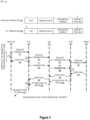
- FIG. 3 depicts a simplified diagrammatic illustration of the transactions handle by SoC subsystems 310, 350 which include TCG unit 320 and TCEP unit 340 to provide asynchronous end-to-end integrity for communications over the NoC subsystem 330.
- SoC subsystems 310, 350 which include TCG unit 320 and TCEP unit 340 to provide asynchronous end-to-end integrity for communications over the NoC subsystem 330.
- the final response message 323 to the initiator subsystem 310 is not held until the PIT response message 334 is received, but is instead issued without delay and then recalled or aborted only later if an interrupt message 324 is issued in the event the PIT response message 334 indicates there was data error during delivery of the regular transaction over the NoC subsystem 330.
- the steps for providing asynchronous end-to-end integrity are very similar to the steps for providing synchronous end-to-end integrity, starting with a first step (1) where the initiator subsystem 310 sends a regular transaction 311, such as a memory access request, to the TCG unit 320.
- the regular transaction may have any suitable message format, such as the depicted regular transaction 301 which is an n-bit message including a user bit field set to first value (e.g., 0), a destination address field, a transaction ID field, and a data field.
- the TCG unit 320 forwards the regular transaction 321 to the NoC subsystem 330.
- the TCG unit 320 sends an "OKAY" final response message 323 to the initiator subsystem 310 without waiting to determine if there was a data error during delivery of the regular transaction over the NoC subsystem 330.
- the TCG unit 320 also generates and forwards a PIT transaction 322 to the NoC subsystem 330 shortly after forwarding the regular transaction 321.
- the PIT transaction may also have any suitable message format, such as the depicted PIT transaction 302 which is a 32-bit message including a user bit field set to second value (e.g., 1), a destination address field, a transaction ID field, and a CRC data field.
- the TCG unit 320 For write transactions, the TCG unit 320 generates the PIT transaction 322 by computing integrity information (e.g., CRC values) from the write address and data fields, and then generating the 32-bit non-modifiable write carrying PIT transaction 322 to include the computed integrity information.
- the TCG unit 320 starts to compute integrity information by storing the read address of the regular transaction for subsequent retrieval, and then generates the 32-bit non-modifiable read PIT transaction 322.
- the TCG unit 320 may include a timer function that measures the time from issuance of the regular transaction 321 to the NoC subsystem 330 until the reception of the PIT response 332 from the NoC subsystem 330. If the timer expires, then the transaction is considered as lost, and the TCG unit 320 triggers an interrupt message 324.
- the TCEP unit 340 After the NoC subsystem 330 receives and forwards the regular transaction 321 and PIT transaction 322 to the TCEP unit 340, respectively, as the regular transaction 331 and PIT transaction 332, the TCEP unit 340 performs the third step (3) by forwarding the regular transaction 341 to the target SoC subsystem 350. In addition, the TCEP unit 340 receives the forwarded PIT transaction 332 and then awaits receipt of the response message 351 from the target SoC subsystem 350 before computing the response message 342 and PIT response message 343. In particular, after receiving the response message 351 from the target SoC subsystem 350, the TCEP unit 340 forwards it as the response message 342 to the NoC subsystem 330.
- the TCEP unit 340 computes a PIT response message 343, where the response message 342 and PIT response message 343 may have any suitable message format that includes, for example, a user bit field, a destination address field, a transaction ID field, and a payload field. As disclosed herein, the contents of the PIT response message fields will depend on the type of regular transaction being protected.
- the TCEP unit 340 may compute the expected integrity protecting information (e.g., local CRC values) from a write address in a first regular transaction 331 and from data contained in the regular transaction(s) 331. To account for regular write transactions that are split by the NoC subsystem 330, the TCEP unit 340 may be configured to continue computing integrity information with data from additional regular transaction(s) 331 until a PIT transaction (e.g., 332) is received that corresponds to the regular transaction (e.g., 331).
- a PIT transaction e.g., 332
- the TCEP 340 Upon receiving the PIT transaction 332, the TCEP 340 checks that the integrity information (e.g., CRC values) received with the PIT transaction 332 corresponds to the local integrity information, and also compares the write address from the PIT transaction 332 with the write address of the first regular transaction 331. If the received integrity information matches the local integrity information and if there is a match between the write addresses of the PIT transaction 332 and first regular transaction 331, the TCEP unit 340 generates the "OKAY" PIT response message 343. However, if they do not match, then the TCEP unit 340 generates the "ERROR" PIT response message 343.
- the integrity information e.g., CRC values
- the TCEP unit 340 may compute the expected integrity information by beginning computation of local integrity information (e.g., local CRC values) using the read address of the regular transaction 331, and then updating the computation of the local integrity information with the read data returned in the read data response message 351 from the target SoC subsystem 350.
- the TCEP unit 340 may be configured to use only the read address from the first regular transaction 331.
- the TCEP unit 340 also forwards read data response message 351 to the NoC subsystem 330 as a forwarded response message 342 along with the PIT response message 343.
- the TCEP unit 340 If the read data response message 351 to the regular transaction 341 is ERROR, then the integrity information is corrupted before being sent to the NoC subsystem 330, in which case the TCEP unit 340 generates the "ERROR” PIT response message 343. Otherwise, the TCEP unit 340 generates the "OKAY" PIT response message 343 which includes the local integrity information (e.g., local CRC values).
- the local integrity information e.g., local CRC values
- the TCG unit 320 After the NoC subsystem 330 receives and forwards the regular response message 333 and PIT response message 334 to the TCG unit 320, the TCG unit 320 performs the fourth step (4) by checking the regular response message 333 and PIT response message 334 received from the NoC subsystem 330 to detect if there was a data error during delivery of the regular transaction over the NoC subsystem 330. If no data error is detected, then the TCG unit 320 does not send any additional response message to the initiator subsystem 310 since the "OKAY" final response message 323 was previously sent to indicate that the regular transaction was successfully transmitted. However, if a data error is detected, then the TCG unit 320 sends an interrupt message 324 to the initiator subsystem 310.
- the TCG unit 320 detects a data error if either the regular response message 333 and/or the PIT response message 334 are ERROR messages, and then issues the interrupt message 324.
- the TCG unit 320 detects a data error by completing or updating the computation of the expected integrity information by retrieving the previously-stored read address from memory (stored at step (2)), and then computing the local integrity protecting information (e.g., local CRC values) for the regular read transaction from the retrieved read address and read data contained in the regular response message 333.
- the local integrity protecting information e.g., local CRC values
- the TCG unit 320 issues the interrupt message 324. In this way, the initiator subsystem 310 obtains the real status of its transaction through an out of band interrupt message 324.
- the integrity information may be computed from the memory access address and data associated with a regular transaction.
- the integrity information may also be computed from any suitable side band information that is supposed to remain invariant during transmission over the NoC subsystem.
- PIT extra protecting information transaction
- an error in the read or write data can be detected as the simplest case since such an error will result in a mismatch between the locally computed integrity information and the integrity information carried by the PIT message.
- the TCG unit When such a mismatch occurs, the TCG unit generates an "ERROR" final write response message (e.g., 223) from the TCG unit to the initiator in the case of synchronous integrity operation.
- the TCG unit generates an interrupt triggered (e.g., 324) by the TCG unit in the case of asynchronous integrity operation.
- an error in the transaction ID that arises during transmission over the NoC subsystem can be detected when the TCEP unit cannot reconcile the received regular transaction with the received PIT transaction.
- the TCEP unit generates an "ERROR" PIT response message (e.g., 243, 343).
- an error in the address that arises during transmission over the NoC subsystem can be detected since the regular transaction and PIT message will not reach the same TCEP unit. For example, if the regular transaction is delivered to a first TCEP unit at a specified address and obtains a response message, that first TCEP unit will never receive associated PIT message if there was an address error. And if the first TCEP unit receives a new regular transaction with its associated PIT message, the first TCEP unit will keep updating the integrity information, thereby triggering a mismatch and an error for this second transaction.
- a second TCEP unit receives the PIT message that was intended to protect the regular transaction but does not also receive the regular transaction, then the second TCEP unit responds to the PIT message by generating an "ERROR" PIT response message (e.g., 243, 343).
- an "ERROR" PIT response message e.g., 243, 343
- an error in the user bit field that arises during transmission over the NoC subsystem can be detected or at least ignored.
- the TCEP unit may be configured to treat any (misidentified) PIT message that is not 32-bits long as a regular transaction by forwarding it to the destination address, resulting in a safe or harmless error.
- the TCEP unit may be configured to treat the (misidentified) PIT message as a PIT message. If there was an ongoing computation of protecting information, then the PIT response generated by the TCEP unit will be based on the state of that computation.
- the TCEP unit will forward the (misidentified) regular transaction to its target destination where any write transaction will corrupt the destination address, and where any read transaction will very likely trigger a mismatch at the TCG unit. Even if these events do not occur, the next regular transaction received by the TCEP unit will generate an error. For example, if the next regular transaction is not the same type (read or write) as the (misidentified) regular transaction, the TCEP unit will detect that that the PIT message for the (misidentified) regular transact was missing. And even if the next regular transaction is the same type (read or write) as the (misidentified) regular transaction, the TCEP unit will continue to update the protecting information while waiting for the PIT message until the timer will be triggered to indicate a data error.
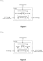
- FIG. 4 depicts a simplified schematic block diagram 400 of a transaction checker generator (TCG) hardware circuit 401 which uses one or more control registers 402 and an Input2NoC protocol converter 406 to convert parity-protected transactions on the input bus 405 to transactions on the NoC bus 407.
- the control registers 402 include TCG input side control logic 403 and TCG NoC side control logic 404 to schedule and check regular transactions and PIT messages received on the input bus 405 for transmission over the NoC bus 407.
- the TCG input side 403 Under control of the control registers 402 configured by the configuration bus, the TCG input side 403 starts computing protecting information when a regular transaction is received, and then notifies the TCG NoC side 404 that there is a PIT message to send. For write access regular transactions, the TCG input side 403 updates the protection information until the write regular transaction is completed, and then notifies the TCG NoC side 404 that a data phase of PIT write message can be sent over the NoC bus 407.
- the TCG input side 403 completes the updating of the protecting information with read data received from the NoC bus 407, and then compares the updated protecting information with the protecting information received on the NoC bus 407 from a PIT response message to determine if there was a data error during delivery of the read access regular transaction over the NoC bus 407.
- the control registers 402 are also configured by the configuration bus to control the TCG NoC side 404 to detect and send a new PIT message that corresponds to the regular transaction by using the same transaction ID and address and that is a non-modifiable transaction.
- the TCG hardware circuit 401 does not add extra cycles on the address and data phase of a regular transaction that flows through the Input2NoC protocol converter 406. The only impact is on the response that is delayed until the PIT response message is received.
- FIG. 5 depicts a simplified schematic block diagram 500 of a transaction checker endpoint (TCEP) hardware circuit 501 which uses one or more control registers 502 and an NoC2Input protocol converter 506 to convert transactions on the NoC bus 505 to parity-protected transactions on the output bus 507.
- the control registers 502 include TCEP NoC input side control logic 503 and TCEP output side control logic 504 to schedule and check regular transactions and PIT messages received on the NoC bus 505 for transmission over the output bus 507.
- the TCEP hardware circuit 501 is the endpoint of PIT messages.
- the TCEP NoC input side 503 of the TCEP hardware circuit 501 computes protecting information based on the received write request and write data from the regular write transaction before notifying the TCEP output side 504 that a regular write transaction can be sent over the output bus 507 to the destination or target subsystem, and then compares the locally computed protecting information to protecting information received in a PIT message corresponding to the regular write transaction that is received on the NoC input bus 505.
- the TCEP output side 504 of the TCEP hardware circuit 501 computes protecting information based on the received read request (received from the regular read transaction) and read data (received from the destination or target subsystem), and then sends the protecting information back to the TCG hardware circuit in the PIT response message.
- the TCEP hardware circuit 501 also generates and checks parity information going along with regular transaction toward its final destination.
- FIG. 6 depicts a simplified flow chart 600 showing a communication sequence of steps performed by a transaction checker generator 601 and transaction checker endpoint 603 when handling write transactions over an interconnect 602 in a synchronous integrity mode to provide end-to-end transaction integrity over the interconnect 602.
- the transaction checker generator 601 may be part of an SoC system in which an initiator subsystem (not shown), such as a Cortex-M4 subsystem, generates one or more write transactions that are transmitted over the interconnect 602.
- the transaction checker endpoint 603 may also be part of the SoC system as part of a destination or target subsystem (not shown), such as a DRAM memory controller subsystem, which is connected to receive and process the write transaction(s).
- the interconnect 602 may be embodied as a standard interconnect, such as, for example, an Intel ® Quick Path Interconnect (QM) interconnect, though any suitable interconnect bus 602 may be used, such as a crossbar switch fabric, for example) that allows the initiator subsystem to access any destination or target subsystem, and that conversely allows data and/or response messages to be returned from any destination or target subsystem to any initiator subsystem.
- QM Quick Path Interconnect
- the transaction checker generator (TCG) 601 receives a write transaction from the initiator subsystem (not shown).
- the write transaction includes a write address, a transaction ID, and write data that are to be written to a destination or target subsystem, such as DRAM memory on the SoC system.
- the TCG 601 forwards the write transaction over the interconnect 602 to the transaction checker endpoint (TCEP) 603.
- the TCG formats the write transaction as a regular write transaction which includes a destination address for the destination or target subsystem, a transaction ID, one or more user bit fields which are set to a first value (e.g., 0b1) to identify the write transaction as a regular transaction, and write data which is to be stored or written to the destination or target subsystem.
- a first value e.g., 0b1
- the TCEP 603 receives the write transaction over the interconnect 602 from the TCG 601.
- the interconnect 602 is a standard interconnect (e.g., one that does not include integrity-protecting logic or circuitry)
- the regular write transaction that is received at the TCEP 603 may include a data error or fault that arose during transmission over the interconnect 602.
- any such error is not detected, and the TCEP 603 forwards the write transaction to the destination or target subsystem as a non-modifiable transaction (step 621).
- the TCG 601 initiates an error detection sequence at step 612 by computing write integrity information from the transmitted regular write transaction.
- the write integrity information may be computed by computing CRC values from the write destination address and transaction ID using the CRC-32 checksum algorithm from ITU-T V.42 protocol.
- the TCEP 603 initiates an error detection sequence at step 622 by computing local integrity information from the received regular write transaction.
- the local integrity information may be computed by computing CRC values from the write destination address and transaction ID using the CRC-32 checksum algorithm from ITU-T V.42 protocol.
- the TCG 601 To enable a comparison of the write and local integrity information, the TCG 601 generates and forwards a write protecting information transaction (PIT) message at step 613 over the interconnect 602 to the TCEP 603.
- the write PIT message sent by the TCG 601 may be formatted to include the write integrity information (CRC) along with the same destination address and transaction ID as the regular write transaction, and to also include the one or more user bit fields which are set to a second value (e.g., 0b0) to identify the message as a PIT message.
- CRC write integrity information
- the TCEP 603 receives the write PIT message (including the write integrity information (CRC)) over the interconnect 602 from the TCG 601.
- the TCEP 603 can compare the write integrity information (computed by the TCG 601) to the local integrity information (computed by the TCEP 603) to see if there is a match, and then generate a PIT response message based on the results of the match comparison. If the write and local integrity information match, then there is no error detected from the transmission of the regular write transaction over the interconnect 602, and the TCEP 603 generates the PIT response message to include a transmission "OK" indication. However, if the write and local integrity information do not match, this indicates that an error occurred during transmission of the regular write transaction over the interconnect 602, in which case the TCEP 603 generates the PIT response message to include a transmission "ERROR" indication.
- CRC write integrity information
- the TCEP 603 receives a write response message from the destination or target subsystem that was generated in response to the write transaction that was forwarded at step 621.
- the write response message from the destination/target subsystem can be received before or after the write integrity information is received and compared to the local integrity information.
- the TCEP 603 forwards the write response message over the interconnect 602 to the TCG 601. If the write response message from the destination/target subsystem indicates there was no error during the write operation, and the TCEP 603 generates the write response message to include a write "OK" indication. However, if the write response message from the destination/target subsystem indicates there was an error during the write operation, and the TCEP 603 generates the write response message to include a write "ERROR" indication.
- the TCEP 603 forwards the PIT response message over the interconnect 602 to the TCG 601.
- the PIT response message includes a transmission "OK” indication if the comparison step 624 indicates that the write and local integrity information match, and includes a transmission "ERROR” indication if the comparison step 624 indicates that the write and local integrity information do not match.
- the write response message can be sent before or after sending the PIT response message.
- the TCG 601 receives the write response message over the interconnect 602 from the TCEP 603. And at step 615, the TCG 601 receives the PIT response message over the interconnect 602 from the TCEP 603. Again, the order of steps 614 and 615 can be reversed.
- the TCG 601 generates and sends an "OK" response message to the initiator subsystem if both the write response and PIT response messages include “OK” indications. However, if either or both of the write response and PIT response messages include an "ERROR” indication, then the TCG 601 generates and sends an "ERROR” response message to the initiator subsystem.
- FIG. 7 depicts a simplified flow chart 700 showing a communication sequence of steps performed by a transaction checker generator 701 and transaction checker endpoint 703 when handling read transactions over an interconnect 702 in a synchronous integrity mode to provide end-to-end transaction integrity over the interconnect 702.
- the transaction checker generator 701 may be part of an SoC system in which an initiator subsystem (not shown), such as a Cortex-M4 subsystem, generates one or more read transactions that are transmitted over the interconnect 702.
- the transaction checker endpoint 703 may also be part of the SoC system as part of a destination or target subsystem (not shown), such as a DRAM memory controller subsystem, which is connected to receive and process the read transaction(s).
- the interconnect 702 may be embodied as a standard interconnect, such as, for example, an Intel ® Quick Path Interconnect (QM) interconnect, though any suitable interconnect bus 702 may be used, such as a crossbar switch fabric, for example) that allows the initiator subsystem to access any destination or target subsystem, and that conversely allows data and/or response messages to be returned from any destination or target subsystem to any initiator subsystem.
- QM Quick Path Interconnect
- the transaction checker generator (TCG) 701 receives a read transaction from the initiator subsystem (not shown).
- the read transaction includes a transaction ID and a read address for memory location for reading or retrieving data at a destination or target subsystem, such as DRAM memory on the SoC system.
- the TCG 701 forwards the read transaction over the interconnect 702 to the transaction checker endpoint (TCEP) 703.
- the TCG 701 formats the read transaction as a regular read transaction which includes a destination address for the destination or target subsystem, a transaction ID, and one or more user bit fields which are set to a first value (e.g., 0b1) to identify the read transaction as a regular read transaction.
- the TCEP 703 receives the read transaction over the interconnect 702 from the TCG 701.
- the interconnect 702 is a standard interconnect (e.g., one that does not include integrity-protecting logic or circuitry)
- the regular read transaction that is received at the TCEP 703 may include a data error or fault that arose during transmission over the interconnect 702.
- any such error is not detected, and the TCEP 703 forwards the read transaction to the destination or target subsystem as a non-modifiable transaction (step 721).
- the TCG 701 In order to detect potential data errors in the regular read transaction that arose during transmission over the interconnect 702, the TCG 701 initiates an error detection sequence at step 712 by storing the read transaction address at the TCG 701 which will be used subsequently to compute a local read integrity information once the read data is retrieved from the destination or target subsystem. In addition, the TCG 701 generates and forwards a read protecting information transaction (PIT) message at step 713 over the interconnect 702 to the TCEP 703.
- PIT read protecting information transaction
- the read PIT message sent by the TCG 701 does not include any read integrity information, but may be formatted to include the same read transaction address and transaction ID as the regular read transaction, and to also include the one or more user bit fields which are set to a second value (e.g., 0b0) to identify the message as a PIT message.
- a second value e.g., 0b0
- the TCEP 703 initiates an error detection sequence at step 722 by starting the computation of read integrity information from the read transaction address.
- the read integrity information may be computed by computing CRC values from the read destination address and transaction ID using the CRC-32 checksum algorithm from ITU-T V.42 protocol, but at this point, the read integrity information is not complete since read data has not been incorporated into the CRC computation.
- the TCEP 703 receives the read PIT message (which does not include the read integrity information) over the interconnect 702 from the TCG 701.
- the TCEP 703 receives a read response message from the destination or target subsystem (not shown) that was generated in response to the read transaction that was forwarded at step 721.
- the read response message from the destination/target subsystem will contain the read data that was requested by the initiator subsystem.
- the read response message can be received before or after the read PIT message is received from the TCG 701 at step 723.
- the TCEP 703 updates the read integrity information using the read data returned from the destination/target subsystem.
- the read integrity information may be updated by computing CRC values from the read destination address, transaction ID, and read data using the CRC-32 checksum algorithm from ITU-T V.42 protocol.
- the TCEP 703 forwards the read response message over the interconnect 702 to the TCG 701. If the read response message from the destination/target subsystem indicates there was no error during the read operation, and the TCEP 703 generates the read response message to include a read "OK" indication. However, if the read response message from the destination/target subsystem indicates there was an error during the read operation, and the TCEP 703 generates the read response message to include a read "ERROR" indication.
- the TCEP 703 generates and forwards a PIT response message over the interconnect 702 to the TCG 701.
- the PIT response message includes the read integrity information which may be computed as a CRC value from the read destination address, transaction ID, and read data.
- the read response message can be sent before or after sending the PIT response message.
- the TCG 701 receives the read response message from the TCEP 703 which includes the read data provided by the destination/target subsystem. And at step 715, the TCG 701 receives the PIT response message from the TCEP 703 which includes the read integrity information computed by the TCEP 703.
- the TCG 701 computes local integrity information from the stored read transaction address and the received read data.
- the local integrity information may be computed by computing CRC values from the read transaction address, transaction ID, and read data (returned in the read response message) using the CRC-32 checksum algorithm from ITU-T V.42 protocol.
- the TCG 701 compares the read integrity information (computed by the TCEP 703) to the local read integrity information (computed by the TCG 701) to see if there is a match. If both the read integrity information (computed by the TCEP 703) and the local read integrity information (computed by the TCG 701) match one another, the TCG 701 generates an "OK" response message to the initiator subsystem. However, if there is not a match between the read integrity information (computed by the TCEP 703) and the local read integrity information (computed by the TCG 701), then the TCG 701 generates and sends an "ERROR" response message to the initiator subsystem.
- FIG. 8 there is shown a simplified schematic diagram of a multi-core system on chip (SoC) 800 having multiple SOC subsystems which are connected to communicate over an interconnect bus 850 by using transaction checker generator units (e.g., 814-816) and transaction checker endpoint units (e.g., 817-819) to provide end-to-end integrity protection over the interconnect bus 850 in accordance with selected embodiments of the present disclosure.
- SoC system on chip
- the SoC subsystems include one or more processor cores 810, 820, 830, 840, each of which may be configured to initiate a transaction request that is sent over the interconnect bus 850 to one of the other SoC subsystems, such as a multi-media accelerator unit 821, a direct memory access (DMA) engine 831, an ethernet/SPI interface engine 841, a high speed serial interface 851, display and camera I/O unit 861, a security module 862, a DRAM controller 863, on-chip M3 memory 864, and/or other hardware devices or modules 871-879.
- DMA direct memory access
- Each of the processor cores 810, 820, 830, 840 may be configured to execute instructions and to process data according to a particular instruction set architecture (ISA), such as x86, PowerPC, SPARC, MIPS, and ARM, for example.
- ISA instruction set architecture
- a highly suitable example of a processor design for the processor core is a Cortex-M4 processor core.
- the processor core may be found in many forms including, for example, any 32-bit or 64-bit microprocessor manufactured by Freescale, Motorola, Intel, AMD, Sun or IBM.
- each of the processor cores 810, 820, 830, 840 may be configured to operate independently of the others, such that all cores may execute in parallel.
- each of cores may be configured to execute multiple threads concurrently, where a given thread may include a set of instructions that may execute independently of instructions from another thread.
- Such a core may also be referred to as a multithreaded (MT) core.
- MT multithreaded
- processor cores refers to any combination of hardware, software, and firmware typically configured to provide a processing functionality with respect to information obtained from or provided to associated circuitry and/or modules (e.g., one or more peripherals, as described below).
- cores include, for example, digital signal processors (DSPs), central processing units (CPUs), microprocessors, and the like.
- DSPs digital signal processors
- CPUs central processing units
- microprocessors and the like.
- masters in that they often act as a bus master with respect to any associated peripherals.
- multi-core refers to any combination of hardware, software, and firmware that that includes two or more such cores (e.g., cores 810 and 820), regardless of whether the individual cores are fabricated monolithically (i.e., on the same chip) or separately.
- a second core may be the same physical core as first core, but has multiple modes of operation (i.e., a core may be virtualized).
- each processor core may include a first level (L1) cache which includes an instruction cache (icache) 811 and a data cache (dcache) 812.
- L1 cache which includes an instruction cache (icache) 811 and a data cache (dcache) 812.
- L2 cache memory L2 cache memory
- the processor core 810 executes instructions and processes data under control of the operating system (OS) which may designate or select the processor core 810 as the control or master node for controlling the workload distribution amongst the processor cores 810, 820, 830, 840.
- OS operating system
- Communication between the cores 810, 820, 830, 840 may be over the interconnect bus 850 or over a crossbar switch and appropriate dual point to point links according to, for example, a split-transaction bus protocol such as the HyperTransport (HT) protocol (not shown).
- HT HyperTransport
- the processor cores 810, 820, 830, 840 may be identically designed or homogenous, different process core designs may be used.
- the multi-core SoC 800 may include one or more additional cores having a different design.
- the depicted multi-core SoC 800 also includes one or more multi-media accelerator units 821 which include one or more graphics processor units (GPU) 822, vector processor units (VPU) 823, and/or audio digital signal processor cores 824.
- GPU graphics processor units
- VPU vector processor units
- Each processor core is coupled across the interconnect bus 850 to communicate with the SoC subsystems 821, 831, 841, 851, 861-864, 871-879.
- Each of the processor cores 810, 820, 830, 840 is in communication over the interconnect bus 850 with the SoC subsystems 821, 831, 841, 851, 861-864, 871-879.
- the interconnect bus 850 may be configured to concurrently accommodate a large number of independent accesses that are processed on each clock cycle, and enables communication data requests from the processor cores 810, 820, 830, 840 to the SoC subsystems 821, 831, 841, 851, 861-864, 871-879, as well as data responses therefrom.
- the interconnect bus 850 may include logic (such as multiplexers or a switch fabric, for example) that allows any core to access any bank of memory with a read or write transaction, and that conversely allows data to be returned from any memory bank to any core.
- the interconnect bus 850 may also include logic to queue data requests and/or responses, such that requests and responses may not block other activity while waiting for service.
- the interconnect bus 850 may be configured as a chip-level arbitration and switching system (CLASS) to arbitrate conflicts that may occur when multiple cores attempt to access a memory or vice versa.
- CLASS chip-level arbitration and switching system
- the interconnect bus 850 is in communication with main memory controller 863 to provide access to the M3 memory 864 or main memory (not shown).
- Memory controller 863 may be configured to manage the transfer of data between the multi-core SoC 800 and system memory, for example.
- multiple instances of memory controller 863 may be implemented, with each instance configured to control a respective bank of system memory.
- Memory controller 863 may be configured to interface to any suitable type of system memory, such as Double Data Rate or Double Data Rate 2 or Double Data Rate 3 Synchronous Dynamic Random Access Memory (DDR/DDR2/ DDR3 SDRAM), or Rambus DRAM (RDRAM), for example.
- memory controller 863 may be configured to support interfacing to multiple different types of system memory.
- the Direct Memory Access (DMA) controller 831 may be provided which controls the direct data transfers to and from system memory via memory controller 863.
- DMA Direct Memory Access
- the multi-core SoC 800 may be configured to receive data from sources other than system memory.
- a network interface engine 841 may be configured to provide a central interface for handling Ethernet and SPI interfaces, thus off-loading the tasks from the cores.
- a high speed serial interface 851 may be configured to support one or more serial RapidIO ports, a PCI-Express Controller, and/or a serial Gigabit Media Independent Interface (SGMII).
- SGMII serial Gigabit Media Independent Interface
- one or more interfaces 870 may be provided which are configured to couple the cores to external boot and/or service devices, such as I/O interrupt concentrators 871, UART device(s) 872, clock(s) 873, timer(s) 874, reset 875, hardware semaphore(s) 876, virtual interrupt(s) 877, Boot ROM 878, I2C interface 879, GPIO ports, and/or other modules.
- I/O interrupt concentrators 871 such as I/O interrupt concentrators 871, UART device(s) 872, clock(s) 873, timer(s) 874, reset 875, hardware semaphore(s) 876, virtual interrupt(s) 877, Boot ROM 878, I2C interface 879, GPIO ports, and/or other modules.
- an initiating subsystem e.g., processing core 810 includes a transaction checker generator (TCG) circuit (e.g., 814) which is configured to send regular transaction messages along with extra protecting information transaction (PIT) messages over the interconnect bus 850 for use in protecting the integrity of the regular transaction messages.
- TCG transaction checker generator
- PIT extra protecting information transaction
- each of the multi-media accelerator units 821 may have its own dedicated TCG circuit.
- other initiating subsystems such as the DMA engine 831 or high-speed serial interface 851, may have its own dedicated TCG circuit 815, 816.
- any target or destination subsystem may include a transaction checker endpoint (TCEP) circuit which is connected and configured to receive the regular transaction messages and PIT messages and to evaluate the integrity of the regular transaction message based on the PIT messages.
- TCEP transaction checker endpoint
- the DRAM controller 863 includes a TCEP circuit 818
- the M3 memory 864 includes a TCEP circuit 819
- the high-speed serial interface 861 includes a TCEP circuit 817.
- TCG circuit e.g., 813
- TCEP circuits e.g., 817, 818, 819
- target SoC subsystem(s) e.g. 851, 863, 864
- the TCG circuit (e.g., 814) generates a regular transaction that is transmitted over the interconnect bus 850, and also generates a PIT message that is transmitted along with the regular transaction over the interconnect bus 850.
- the TCG circuit computes protecting information that is included in the PIT message and sent over the interconnect bus 850 to the destination subsystem.
- the TCG circuit computes local protecting information based on the read address and transaction ID for the regular read transaction and based on the read data that is returned to the TCG circuit by the destination subsystem over the interconnect bus 850.
- the TCG circuit also handles the responses to the regular transaction and the PIT response (PITR).
- a TCEP circuit (e.g., 818) is configured to process the regular transactions received over the interconnect bus 850, and to compute the response to the PIT transaction for transmission over the interconnect 850 to the initiator SoC subsystem.
- the TCEP circuit (e.g., 818) that receives a regular write transaction may compute local protecting information (e.g., CRC data) based on received write address, transaction ID, and write data in the regular write transaction, and then compare the computed local protecting information to the protecting information received in the PIT message from the TCG circuit.
- local protecting information e.g., CRC data
- the TCEP circuit that receives a regular read transaction may compute protecting information (e.g., CRC data) based on the received read address, transaction ID, and received read data, and then send the protecting information back to the originating TCG circuit where it is compared to a locally computed protecting information.
- protecting information e.g., CRC data
- the network interconnect may be a network-on-chip (NoC) bus.
- the network interconnect is a non-safety aware network-on-chip (NoC) bus which does not include built-in integrity protection structures.
- the network interconnect may be a Compute Express Link (CXL) interconnect.
- the SoC apparatus includes an initiator SoC subsystem, such as a processor core subsystem, that is configured to send a regular transaction message over the network interconnect and to receive a regular transaction response message from the network interconnect, where the regular transaction message and regular transaction response message do not include integrity values.
- the SoC apparatus includes a target SoC subsystem, such as a memory controller subsystem, that is configured to receive the regular transaction message from the network interconnect and to send the regular transaction response message over the network interconnect to the initiator SoC subsystem.
- the SoC apparatus also includes a first integrity module connected between the initiator SoC subsystem and network interconnect, where the first integrity module is configured to compute a first integrity value based on the regular transaction message or the regular transaction response message and to send a protecting information transaction (PIT) message over the network interconnect to the target SoC subsystem.
- the regular transaction message and the PIT message each include a memory address field, a transaction ID field, and a user bit field having a first value for the regular transaction message or a second value for the PIT message.
- the SoC apparatus includes a second integrity module connected between the network interconnect and the target Soc subsystem, where the second integrity module is configured to compute a second integrity value based on the regular transaction message or the regular transaction response message and to send a PIT response message over the network interconnect to the initiator SoC subsystem.
- the first integrity value and second integrity value are each cyclic redundancy check (CRC) values computed from information contained in the memory address field and transaction ID field and from information contained in the regular transaction message or regular transaction response message.
- CRC cyclic redundancy check
- the SoC apparatus also includes a compatibility module configured to compare the first and second integrity values to verify the end-to-end integrity of the regular transaction message or the regular transaction response message sent over the network interconnect.
- the first integrity module is configured to send the first integrity value in the PIT message sent over the network interconnect to the target SoC subsystem;
- the second integrity module is configured to compute the second integrity value based on a write address, transaction ID, and write data from the regular write transaction message;
- the compatibility module is included in the second integrity module and configured to compare the first and second integrity values to verify the end-to-end integrity of the regular write transaction message sent over the network interconnect.
- the second integrity module is configured to send read data in a regular read transaction response message over the network interconnect to the initiator SoC subsystem and to include the second integrity value in the PIT response message sent over the network interconnect to the initiator SoC subsystem;
- the first integrity module is configured to compute the first integrity value based on a read address, transaction ID, and read data from the regular read transaction response message;
- the compatibility module is included in the first integrity module and configured to compare the first and second integrity values to verify the end-to-end integrity of the regular read transaction message sent over the network interconnect.
- SoC system-on-chip
- a first integrity module receives a regular write transaction message generated by an initiator SoC subsystem (e.g., a processor core subsystem), where the regular write transaction message includes a write address and data for a target SoC subsystem (e.g., a memory controller subsystem) and does do not include integrity values.
- an initiator SoC subsystem e.g., a processor core subsystem
- the regular write transaction message includes a write address and data for a target SoC subsystem (e.g., a memory controller subsystem) and does do not include integrity values.
- target SoC subsystem e.g., a memory controller subsystem
- the first integrity module forwards the regular write transaction message over the SoC network interconnect to a second integrity module which is connected between the network interconnect and the target Soc subsystem, where the second integrity module forwards the regular write transaction message for write processing by the target SoC subsystem to return a write response message to the second integrity module.
- a first integrity value is computed based on the write address and data received by the first integrity module in the regular write transaction message.
- the first integrity module generates a write protecting information transaction (PIT) message which includes the first integrity value, and then send the write PIT message over the SoC network interconnect to the second integrity module.
- PIT write protecting information transaction
- the regular write transaction message and the write PIT message each include a memory address field, a write data field, a transaction ID field, and a user bit field having a first value for the regular write transaction message or a second value for the write PIT message.
- a second integrity value is computed based on the write address and data included in the regular write transaction message received over the network interconnect.
- the first integrity value and second integrity value are each cyclic redundancy check (CRC) values computed from information contained in the memory address field, write data field, and transaction ID field.
- CRC cyclic redundancy check
- the second integrity module compares the first integrity value to the second integrity value to detect if there is a match between the first and second integrity values.
- the second integrity module If there is a match between the first and second integrity values, the second integrity module generates a PIT response message having a first value indicating there is end-to-end integrity of communications over the SoC network interconnect. And if there is not a match between the first and second integrity values, the second integrity module generates a PIT response message having second value indicating there is not end-to-end integrity of communications over the SoC network interconnect. Subsequently, the second integrity module forwards the write response message over the SoC network interconnect to first integrity module, and also sends the PIT response message over the SoC network interconnect to the first integrity module. At the first integrity module, a regular write transaction response message is generated that is sent to the initiator SoC subsystem.
- the regular write transaction response message is generated in response to at least the PIT response message and the write response message. In other embodiments, the regular write transaction response message is generated prior to receiving the PIT response message from the second integrity module, and the first integrity module subsequently generates an interrupt message that is sent to the initiator SoC subsystem in response to the PIT response message having the second value.
- SoC system-on-chip
- a first integrity module receives a regular read transaction message generated by an initiator SoC subsystem, where the regular read transaction message includes a read address for a target SoC subsystem, but does not include integrity values.
- the first integrity module forwards the regular read transaction message over the SoC network interconnect to a second integrity module which is connected between the network interconnect and the target Soc subsystem, where the second integrity module forwards the regular read transaction message for read processing by the target SoC subsystem to return a read response message comprising read data to the second integrity module.
- the read address from the regular read transaction message is stored.
- the first integrity module generates and sends a read protecting information transaction (PIT) message over the SoC network interconnect to the second integrity module.
- PIT read protecting information transaction
- the regular read transaction message and the read PIT message each include a memory address field, a transaction ID field, and a user bit field having a first value for the regular read transaction message or a second value for the read PIT message.
- a first integrity value is computed based on the read address and read data included in the read response message received from the target SoC subsystem.
- the first integrity value is computed as a first cyclic redundancy check (CRC) value from information contained in the memory address field and transaction ID field of the regular read transaction message and from read data included in the read response message received from the target SoC subsystem.
- CRC cyclic redundancy check
- the second integrity module generates a PIT response message which includes the first integrity value, and then sends the PIT response message (and first integrity value) over the SoC network interconnect to the first integrity module.
- the second integrity module also forwards the read response message over the SoC network interconnect to first integrity module.
- the first integrity module Based on the read address stored at the first integrity module and the read data in the read response message received by the first integrity module, the first integrity module computes a second integrity value.
- the second integrity value is computed as a second cyclic redundancy check (CRC) value from information contained in the memory address field and transaction ID field of the regular read transaction message and from read data included in the PIT response message received from the second integrity module.
- CRC cyclic redundancy check
- the first integrity module also compares the first integrity value to the second integrity value to detect if there is a match between the first and second integrity values. If there is a match between the first and second integrity values, the first integrity module generates a regular read transaction response message having a first value indicating there is end-to-end integrity of communications over the SoC network interconnect. But if there is not a match between the first and second integrity values, the first integrity module generates a regular read transaction response message having a second value indicating there is not end-to-end integrity of communications over the SoC network interconnect.
- the regular read transaction response message is generated in response to at least the PIT response message and the read response message received at the first integrity module. In other embodiments, the regular read transaction response message is generated prior to receiving the PIT response message from the second integrity module, and the first integrity module subsequently generates an interrupt message that is sent to the initiator SoC subsystem in response to the PIT response message having the second value.
- FIG. 1 illustrates an exemplary SoC architecture in which different SoC subsystems include transaction checker generator or transaction checker endpoints circuits to provide end-to-end integrity protection over the interconnect subsystem
- FIG. 1 describes an exemplary SoC architecture in which different SoC subsystems include transaction checker generator or transaction checker endpoints circuits to provide end-to-end integrity protection over the interconnect subsystem
- this exemplary architecture is presented merely to provide a useful reference in discussing various aspects of the invention. Description of the architecture has been simplified for purposes of discussion, and it is just one of many different types of appropriate architectures that may be used in accordance with the present disclosure.
- Those skilled in the art will recognize that the boundaries between logic blocks are merely illustrative and that alternative embodiments may merge logic blocks or circuit elements or impose an alternate decomposition of functionality upon various logic blocks or circuit elements.
- any two components herein combined to achieve a particular functionality can be seen as “associated with” each other such that the desired functionality is achieved, irrespective of architectures or intermedial components.
- any two components so associated can also be viewed as being “operably connected,” or “operably coupled,” to each other to achieve the desired functionality.
- the example SoC system embodiments illustrated in Figures 1 and 8 may be implemented with circuitry located on a single integrated circuit or within a same device.
- the SoC system embodiments may include any number of separate integrated circuits or separate devices interconnected with each other.
- the main memory 864 may be located in whole or in part on the same integrated circuit as the SoC control CPU 810 or on a separate integrated circuit or located within another peripheral or slave discretely separate from other elements of SoC system 800.
- Peripherals 871-879 may also be located in whole or in part on separate integrated circuits or devices.
- the transaction integrity system disclosed herein may be used with systems which spread over several SoCs.
- Compute Express Link is an interconnect specification used with CPU-to-Device and CPU-to-Memory designs which is not necessarily end to end it simply looks like a on chip NOC.
- a first integrity module TCG
- TCEP second integrity module
- SoC system-on-chip
- the SoC includes an initiator subsystem connected over the network interconnect to a target subsystem
- a first integrity module is configured to compute a first integrity value based on regular transaction messages sent or received by the initiator subsystem and to send a protecting information transaction (PIT) message over the network interconnect to the target subsystem
- PIT protecting information transaction
- a second integrity module is configured to compute a second integrity value based on regular transaction messages sent or received by the destination subsystem and to send a PIT response message over the network interconnect to the initiator subsystem
- a compatibility module compares the first and second integrity values to verify the end-to-end integrity of the regular transaction messages sent or received over the network interconnect.
- All or some of the software described herein may be received from elements of the SoC system, such as, for example, from computer readable media such as memory 864 or other media on other computer systems.
- computer readable media such as memory 864 or other media on other computer systems.
- Such computer readable media may be permanently, removably or remotely coupled to an information processing system, such as the SoC system 800.
- the computer readable media may include, for example and without limitation, any number of the following: magnetic storage media including disk and tape storage media; optical storage media such as compact disk media (e.g., CD-ROM, CD-R, etc.) and digital video disk storage media; nonvolatile memory storage media including semiconductor-based memory units such as FLASH memory, EEPROM, EPROM, ROM; ferromagnetic digital memories; MRAM; volatile storage media including registers, buffers or caches, main memory, RAM, etc.; and data transmission media including computer networks, point-to-point telecommunication equipment, and carrier wave transmission media, just to name a few.
- magnetic storage media including disk and tape storage media
- optical storage media such as compact disk media (e.g., CD-ROM, CD-R, etc.) and digital video disk storage media
- nonvolatile memory storage media including semiconductor-based memory units such as FLASH memory, EEPROM, EPROM, ROM
- ferromagnetic digital memories such as FLASH memory, EEPROM, EPROM, ROM
- the SoC systems disclosed herein are part of a computer system such as an embedded microcontroller.
- Other embodiments may include different types of computer systems.
- Computer systems are information handling systems which can be designed to give independent computing power to one or more users. Computer systems may be found in many forms.
- a typical computer system includes at least one processing unit, associated memory and a number of input/output (I/O) devices.
- a computer system processes information according to a program and produces resultant output information via I/O devices.
- a program is a list of instructions such as a particular application program and/or an operating system.
- a computer program is typically stored internally on computer readable storage medium or transmitted to the computer system via a computer readable transmission medium.
- a computer process typically includes an executing program or portion of a program, current program values and state information, and the resources used by the operating system to manage the execution of the process.
- a parent process may spawn other, child processes to help perform the overall functionality of the parent process. Because the parent process specifically spawns the child processes to perform a portion of the overall functionality of the parent process, the functions performed by child processes (and grandchild processes, etc.) may sometimes be described as being performed by the parent process.
- program is defined as a sequence of instructions designed for execution on a computer system.
- a program, or computer program may include a subroutine, a function, a procedure, an object method, an object implementation, an executable application, an applet, a servlet, a source code, an object code, a shared library/dynamic load library and/or other sequence of instructions designed for execution on a computer system.
- the terms “comprises,” “comprising,” or any other variation thereof, are intended to cover a non-exclusive inclusion, such that a process, method, article, or apparatus that comprises a list of elements does not include only those elements but may include other elements not expressly listed or inherent to such process, method, article, or apparatus.
- the terms “a” or “an,” as used herein, are defined as one or more than one.
Landscapes
- Engineering & Computer Science (AREA)
- Theoretical Computer Science (AREA)
- General Engineering & Computer Science (AREA)
- Computer Security & Cryptography (AREA)
- Computer Hardware Design (AREA)
- Physics & Mathematics (AREA)
- General Physics & Mathematics (AREA)
- Signal Processing (AREA)
- Computer Networks & Wireless Communication (AREA)
- Quality & Reliability (AREA)
- Computing Systems (AREA)
- Health & Medical Sciences (AREA)
- Bioethics (AREA)
- General Health & Medical Sciences (AREA)
- Software Systems (AREA)
- Microelectronics & Electronic Packaging (AREA)
- Data Exchanges In Wide-Area Networks (AREA)
- Hardware Redundancy (AREA)
Priority Applications (3)
| Application Number | Priority Date | Filing Date | Title |
|---|---|---|---|
| EP22306293.6A EP4332809B1 (de) | 2022-08-31 | 2022-08-31 | End-to-end-transaktionsintegrität durch standardverbindung |
| US18/317,494 US12261691B2 (en) | 2022-08-31 | 2023-05-15 | End-to-end transaction integrity through standard interconnect |
| CN202311104667.1A CN117640132A (zh) | 2022-08-31 | 2023-08-30 | 经由标准互连件的端到端事务完整性 |
Applications Claiming Priority (1)
| Application Number | Priority Date | Filing Date | Title |
|---|---|---|---|
| EP22306293.6A EP4332809B1 (de) | 2022-08-31 | 2022-08-31 | End-to-end-transaktionsintegrität durch standardverbindung |
Publications (2)
| Publication Number | Publication Date |
|---|---|
| EP4332809A1 true EP4332809A1 (de) | 2024-03-06 |
| EP4332809B1 EP4332809B1 (de) | 2025-09-24 |
Family
ID=84331291
Family Applications (1)
| Application Number | Title | Priority Date | Filing Date |
|---|---|---|---|
| EP22306293.6A Active EP4332809B1 (de) | 2022-08-31 | 2022-08-31 | End-to-end-transaktionsintegrität durch standardverbindung |
Country Status (3)
| Country | Link |
|---|---|
| US (1) | US12261691B2 (de) |
| EP (1) | EP4332809B1 (de) |
| CN (1) | CN117640132A (de) |
Families Citing this family (1)
| Publication number | Priority date | Publication date | Assignee | Title |
|---|---|---|---|---|
| DE102024202022A1 (de) * | 2024-03-05 | 2025-09-11 | Robert Bosch Gesellschaft mit beschränkter Haftung | Verfahren und Vorrichtung zum Erkennen einer Verfälschung beim Kommunizieren zwischen Komponenten eines Systems mit Anforderungen an dessen funktionale Sicherheit |
Citations (3)
| Publication number | Priority date | Publication date | Assignee | Title |
|---|---|---|---|---|
| US20200328879A1 (en) * | 2019-08-13 | 2020-10-15 | Intel Corporation | Secure communications over computer buses |
| US20210089388A1 (en) * | 2020-07-14 | 2021-03-25 | Intel Corporation | System, Apparatus And Method For Providing Protection Against Silent Data Corruption In A Link |
| US20210336767A1 (en) * | 2021-06-25 | 2021-10-28 | Intel Corporation | Memory bus integrity and data encryption (ide) |
Family Cites Families (10)
| Publication number | Priority date | Publication date | Assignee | Title |
|---|---|---|---|---|
| US20020091976A1 (en) * | 2001-01-09 | 2002-07-11 | Lee Whay Sing | Reverse parity coding |
| US20020144209A1 (en) * | 2001-02-20 | 2002-10-03 | Cute Ltd. | System for enhanced error correction in trellis decoding |
| US7065702B2 (en) * | 2001-04-12 | 2006-06-20 | Siliquent Technologies Ltd. | Out-of-order calculation of error detection codes |
| DE60208062T2 (de) * | 2001-06-01 | 2006-08-03 | Koninklijke Philips Electronics N.V. | Digitales system und entsprechendes verfahren zur fehlererkennung |
| KR100539864B1 (ko) * | 2001-07-25 | 2005-12-28 | 삼성전자주식회사 | 부호분할다중접속 이동통신시스템에서 고속 데이터의 재전송장치 및 방법 |
| CA3023907C (en) * | 2004-09-25 | 2019-06-04 | Tq Delta, Llc | Crc counter normalization |
| US7562284B2 (en) | 2005-08-26 | 2009-07-14 | International Business Machines Corporation | Apparatus, system, and method for mandatory end to end integrity checking in a storage system |
| US20090210770A1 (en) * | 2008-02-14 | 2009-08-20 | International Business Machines Corporation | Method, system and computer program product for end to end error checking in ethernet |
| EP3926452A1 (de) | 2020-06-19 | 2021-12-22 | NXP USA, Inc. | Norflash-teilung |
| JP7188416B2 (ja) | 2020-06-22 | 2022-12-13 | トヨタ自動車株式会社 | データ収集装置およびデータ収集方法 |
-
2022
- 2022-08-31 EP EP22306293.6A patent/EP4332809B1/de active Active
-
2023
- 2023-05-15 US US18/317,494 patent/US12261691B2/en active Active
- 2023-08-30 CN CN202311104667.1A patent/CN117640132A/zh active Pending
Patent Citations (3)
| Publication number | Priority date | Publication date | Assignee | Title |
|---|---|---|---|---|
| US20200328879A1 (en) * | 2019-08-13 | 2020-10-15 | Intel Corporation | Secure communications over computer buses |
| US20210089388A1 (en) * | 2020-07-14 | 2021-03-25 | Intel Corporation | System, Apparatus And Method For Providing Protection Against Silent Data Corruption In A Link |
| US20210336767A1 (en) * | 2021-06-25 | 2021-10-28 | Intel Corporation | Memory bus integrity and data encryption (ide) |
Also Published As
| Publication number | Publication date |
|---|---|
| US20240070018A1 (en) | 2024-02-29 |
| CN117640132A (zh) | 2024-03-01 |
| EP4332809B1 (de) | 2025-09-24 |
| US12261691B2 (en) | 2025-03-25 |
Similar Documents
| Publication | Publication Date | Title |
|---|---|---|
| US9823983B2 (en) | Electronic fault detection unit | |
| CN102246155B (zh) | 多处理器数据处理系统中的错误检测 | |
| JP7351933B2 (ja) | エラーリカバリ方法及び装置 | |
| US9052887B2 (en) | Fault tolerance of data processing steps operating in either a parallel operation mode or a non-synchronous redundant operation mode | |
| TWI566088B (zh) | 標頭同位錯誤處置技術 | |
| US4939643A (en) | Fault tolerant digital data processor with improved bus protocol | |
| CN104572517B (zh) | 提供被请求数据的方法、控制器以及计算机系统 | |
| US4438494A (en) | Apparatus of fault-handling in a multiprocessing system | |
| US5640508A (en) | Fault detecting apparatus for a microprocessor system | |
| KR102413593B1 (ko) | 교착상태 방지를 위한 방법들 및 회로들 | |
| US10691527B2 (en) | System interconnect and system on chip having the same | |
| US6678838B1 (en) | Method to track master contribution information in a write buffer | |
| US20120311373A1 (en) | Sideband error signaling | |
| US10042692B1 (en) | Circuit arrangement with transaction timeout detection | |
| WO2024131845A1 (zh) | 一种片上系统以及汽车 | |
| US12261691B2 (en) | End-to-end transaction integrity through standard interconnect | |
| US7194671B2 (en) | Mechanism handling race conditions in FRC-enabled processors | |
| EP3321814B1 (de) | Verfahren und vorrichtung zur handhabung offener verbindungstransaktionen | |
| US7631226B2 (en) | Computer system, bus controller, and bus fault handling method used in the same computer system and bus controller | |
| US9231618B2 (en) | Early data tag to allow data CRC bypass via a speculative memory data return protocol | |
| US20190050362A1 (en) | Integrated input/output management | |
| CN114594991A (zh) | 硬件加速器设备、对应的系统和操作方法 | |
| EP1714214A1 (de) | Vorrichtung und verfahren zum aufrechterhalten der datenintegrität nach paritätsfehlerdetektion | |
| CN119493663A (zh) | 一种双cpu同步系统及方法、cpu执行中断服务的方法 | |
| CN118760556A (zh) | 芯片内通信总线的验证方法、装置、存储介质、处理器和程序产品 |
Legal Events
| Date | Code | Title | Description |
|---|---|---|---|
| PUAI | Public reference made under article 153(3) epc to a published international application that has entered the european phase |
Free format text: ORIGINAL CODE: 0009012 |
|
| STAA | Information on the status of an ep patent application or granted ep patent |
Free format text: STATUS: THE APPLICATION HAS BEEN PUBLISHED |
|
| AK | Designated contracting states |
Kind code of ref document: A1 Designated state(s): AL AT BE BG CH CY CZ DE DK EE ES FI FR GB GR HR HU IE IS IT LI LT LU LV MC MK MT NL NO PL PT RO RS SE SI SK SM TR |
|
| STAA | Information on the status of an ep patent application or granted ep patent |
Free format text: STATUS: REQUEST FOR EXAMINATION WAS MADE |
|
| 17P | Request for examination filed |
Effective date: 20240906 |
|
| RBV | Designated contracting states (corrected) |
Designated state(s): AL AT BE BG CH CY CZ DE DK EE ES FI FR GB GR HR HU IE IS IT LI LT LU LV MC MK MT NL NO PL PT RO RS SE SI SK SM TR |
|
| GRAP | Despatch of communication of intention to grant a patent |
Free format text: ORIGINAL CODE: EPIDOSNIGR1 |
|
| STAA | Information on the status of an ep patent application or granted ep patent |
Free format text: STATUS: GRANT OF PATENT IS INTENDED |
|
| RIC1 | Information provided on ipc code assigned before grant |
Ipc: G06F 13/00 20060101ALI20250328BHEP Ipc: G06F 21/64 20130101ALI20250328BHEP Ipc: G06F 11/08 20060101ALI20250328BHEP Ipc: G06F 21/60 20130101AFI20250328BHEP |
|
| INTG | Intention to grant announced |
Effective date: 20250410 |
|
| GRAS | Grant fee paid |
Free format text: ORIGINAL CODE: EPIDOSNIGR3 |
|
| GRAA | (expected) grant |
Free format text: ORIGINAL CODE: 0009210 |
|
| STAA | Information on the status of an ep patent application or granted ep patent |
Free format text: STATUS: THE PATENT HAS BEEN GRANTED |
|
| AK | Designated contracting states |
Kind code of ref document: B1 Designated state(s): AL AT BE BG CH CY CZ DE DK EE ES FI FR GB GR HR HU IE IS IT LI LT LU LV MC MK MT NL NO PL PT RO RS SE SI SK SM TR |
|
| REG | Reference to a national code |
Ref country code: GB Ref legal event code: FG4D |
|
| REG | Reference to a national code |
Ref country code: CH Ref legal event code: EP |
|
| REG | Reference to a national code |
Ref country code: DE Ref legal event code: R096 Ref document number: 602022021924 Country of ref document: DE |
|
| REG | Reference to a national code |
Ref country code: IE Ref legal event code: FG4D |
|
| PG25 | Lapsed in a contracting state [announced via postgrant information from national office to epo] |
Ref country code: NO Free format text: LAPSE BECAUSE OF FAILURE TO SUBMIT A TRANSLATION OF THE DESCRIPTION OR TO PAY THE FEE WITHIN THE PRESCRIBED TIME-LIMIT Effective date: 20251224 |
|
| REG | Reference to a national code |
Ref country code: LT Ref legal event code: MG9D |
|
| PG25 | Lapsed in a contracting state [announced via postgrant information from national office to epo] |
Ref country code: FI Free format text: LAPSE BECAUSE OF FAILURE TO SUBMIT A TRANSLATION OF THE DESCRIPTION OR TO PAY THE FEE WITHIN THE PRESCRIBED TIME-LIMIT Effective date: 20250924 |
|
| PG25 | Lapsed in a contracting state [announced via postgrant information from national office to epo] |
Ref country code: HR Free format text: LAPSE BECAUSE OF FAILURE TO SUBMIT A TRANSLATION OF THE DESCRIPTION OR TO PAY THE FEE WITHIN THE PRESCRIBED TIME-LIMIT Effective date: 20250924 |
|
| PG25 | Lapsed in a contracting state [announced via postgrant information from national office to epo] |
Ref country code: GR Free format text: LAPSE BECAUSE OF FAILURE TO SUBMIT A TRANSLATION OF THE DESCRIPTION OR TO PAY THE FEE WITHIN THE PRESCRIBED TIME-LIMIT Effective date: 20251225 |
|
| PG25 | Lapsed in a contracting state [announced via postgrant information from national office to epo] |
Ref country code: SE Free format text: LAPSE BECAUSE OF FAILURE TO SUBMIT A TRANSLATION OF THE DESCRIPTION OR TO PAY THE FEE WITHIN THE PRESCRIBED TIME-LIMIT Effective date: 20250924 |
|
| PG25 | Lapsed in a contracting state [announced via postgrant information from national office to epo] |
Ref country code: LV Free format text: LAPSE BECAUSE OF FAILURE TO SUBMIT A TRANSLATION OF THE DESCRIPTION OR TO PAY THE FEE WITHIN THE PRESCRIBED TIME-LIMIT Effective date: 20250924 |
|
| PG25 | Lapsed in a contracting state [announced via postgrant information from national office to epo] |
Ref country code: BG Free format text: LAPSE BECAUSE OF FAILURE TO SUBMIT A TRANSLATION OF THE DESCRIPTION OR TO PAY THE FEE WITHIN THE PRESCRIBED TIME-LIMIT Effective date: 20250924 |
|
| PG25 | Lapsed in a contracting state [announced via postgrant information from national office to epo] |
Ref country code: RS Free format text: LAPSE BECAUSE OF FAILURE TO SUBMIT A TRANSLATION OF THE DESCRIPTION OR TO PAY THE FEE WITHIN THE PRESCRIBED TIME-LIMIT Effective date: 20251224 |
|
| REG | Reference to a national code |
Ref country code: NL Ref legal event code: MP Effective date: 20250924 |
|
| PG25 | Lapsed in a contracting state [announced via postgrant information from national office to epo] |
Ref country code: NL Free format text: LAPSE BECAUSE OF FAILURE TO SUBMIT A TRANSLATION OF THE DESCRIPTION OR TO PAY THE FEE WITHIN THE PRESCRIBED TIME-LIMIT Effective date: 20250924 |
|
| REG | Reference to a national code |
Ref country code: AT Ref legal event code: MK05 Ref document number: 1840922 Country of ref document: AT Kind code of ref document: T Effective date: 20250924 |
|
| PG25 | Lapsed in a contracting state [announced via postgrant information from national office to epo] |
Ref country code: SM Free format text: LAPSE BECAUSE OF FAILURE TO SUBMIT A TRANSLATION OF THE DESCRIPTION OR TO PAY THE FEE WITHIN THE PRESCRIBED TIME-LIMIT Effective date: 20250924 |
|
| PG25 | Lapsed in a contracting state [announced via postgrant information from national office to epo] |
Ref country code: ES Free format text: LAPSE BECAUSE OF FAILURE TO SUBMIT A TRANSLATION OF THE DESCRIPTION OR TO PAY THE FEE WITHIN THE PRESCRIBED TIME-LIMIT Effective date: 20250924 |
|
| PG25 | Lapsed in a contracting state [announced via postgrant information from national office to epo] |
Ref country code: AT Free format text: LAPSE BECAUSE OF FAILURE TO SUBMIT A TRANSLATION OF THE DESCRIPTION OR TO PAY THE FEE WITHIN THE PRESCRIBED TIME-LIMIT Effective date: 20250924 |
|
| PG25 | Lapsed in a contracting state [announced via postgrant information from national office to epo] |
Ref country code: IT Free format text: LAPSE BECAUSE OF FAILURE TO SUBMIT A TRANSLATION OF THE DESCRIPTION OR TO PAY THE FEE WITHIN THE PRESCRIBED TIME-LIMIT Effective date: 20250924 |
|
| PG25 | Lapsed in a contracting state [announced via postgrant information from national office to epo] |
Ref country code: IS Free format text: LAPSE BECAUSE OF FAILURE TO SUBMIT A TRANSLATION OF THE DESCRIPTION OR TO PAY THE FEE WITHIN THE PRESCRIBED TIME-LIMIT Effective date: 20260124 |
|
| PG25 | Lapsed in a contracting state [announced via postgrant information from national office to epo] |
Ref country code: CZ Free format text: LAPSE BECAUSE OF FAILURE TO SUBMIT A TRANSLATION OF THE DESCRIPTION OR TO PAY THE FEE WITHIN THE PRESCRIBED TIME-LIMIT Effective date: 20250924 Ref country code: PT Free format text: LAPSE BECAUSE OF FAILURE TO SUBMIT A TRANSLATION OF THE DESCRIPTION OR TO PAY THE FEE WITHIN THE PRESCRIBED TIME-LIMIT Effective date: 20260126 |
|
| PG25 | Lapsed in a contracting state [announced via postgrant information from national office to epo] |
Ref country code: PL Free format text: LAPSE BECAUSE OF FAILURE TO SUBMIT A TRANSLATION OF THE DESCRIPTION OR TO PAY THE FEE WITHIN THE PRESCRIBED TIME-LIMIT Effective date: 20250924 |
|
| PG25 | Lapsed in a contracting state [announced via postgrant information from national office to epo] |
Ref country code: SK Free format text: LAPSE BECAUSE OF FAILURE TO SUBMIT A TRANSLATION OF THE DESCRIPTION OR TO PAY THE FEE WITHIN THE PRESCRIBED TIME-LIMIT Effective date: 20250924 Ref country code: EE Free format text: LAPSE BECAUSE OF FAILURE TO SUBMIT A TRANSLATION OF THE DESCRIPTION OR TO PAY THE FEE WITHIN THE PRESCRIBED TIME-LIMIT Effective date: 20250924 |