EP4332821A1 - Entwurfsverfahren und -system für gleichstromschleifenimpedanz - Google Patents
Entwurfsverfahren und -system für gleichstromschleifenimpedanz Download PDFInfo
- Publication number
- EP4332821A1 EP4332821A1 EP21941589.0A EP21941589A EP4332821A1 EP 4332821 A1 EP4332821 A1 EP 4332821A1 EP 21941589 A EP21941589 A EP 21941589A EP 4332821 A1 EP4332821 A1 EP 4332821A1
- Authority
- EP
- European Patent Office
- Prior art keywords
- impedance
- loop
- parameters
- hvdc
- hvdc system
- Prior art date
- Legal status (The legal status is an assumption and is not a legal conclusion. Google has not performed a legal analysis and makes no representation as to the accuracy of the status listed.)
- Pending
Links
Images

Classifications
-
- G—PHYSICS
- G06—COMPUTING OR CALCULATING; COUNTING
- G06F—ELECTRIC DIGITAL DATA PROCESSING
- G06F30/00—Computer-aided design [CAD]
- G06F30/30—Circuit design
- G06F30/36—Circuit design at the analogue level
- G06F30/367—Design verification, e.g. using simulation, simulation program with integrated circuit emphasis [SPICE], direct methods or relaxation methods
-
- G—PHYSICS
- G06—COMPUTING OR CALCULATING; COUNTING
- G06F—ELECTRIC DIGITAL DATA PROCESSING
- G06F30/00—Computer-aided design [CAD]
- G06F30/30—Circuit design
- G06F30/39—Circuit design at the physical level
- G06F30/394—Routing
- G06F30/3947—Routing global
-
- G—PHYSICS
- G06—COMPUTING OR CALCULATING; COUNTING
- G06F—ELECTRIC DIGITAL DATA PROCESSING
- G06F30/00—Computer-aided design [CAD]
- G06F30/30—Circuit design
- G06F30/36—Circuit design at the analogue level
- G06F30/373—Design optimisation
-
- G—PHYSICS
- G06—COMPUTING OR CALCULATING; COUNTING
- G06F—ELECTRIC DIGITAL DATA PROCESSING
- G06F30/00—Computer-aided design [CAD]
- G06F30/20—Design optimisation, verification or simulation
- G06F30/27—Design optimisation, verification or simulation using machine learning, e.g. artificial intelligence, neural networks, support vector machines [SVM] or training a model
-
- G—PHYSICS
- G06—COMPUTING OR CALCULATING; COUNTING
- G06F—ELECTRIC DIGITAL DATA PROCESSING
- G06F30/00—Computer-aided design [CAD]
- G06F30/30—Circuit design
- G06F30/39—Circuit design at the physical level
- G06F30/398—Design verification or optimisation, e.g. using design rule check [DRC], layout versus schematics [LVS] or finite element methods [FEM]
-
- G—PHYSICS
- G06—COMPUTING OR CALCULATING; COUNTING
- G06F—ELECTRIC DIGITAL DATA PROCESSING
- G06F2111/00—Details relating to CAD techniques
- G06F2111/06—Multi-objective optimisation, e.g. Pareto optimisation using simulated annealing [SA], ant colony algorithms or genetic algorithms [GA]
-
- G—PHYSICS
- G06—COMPUTING OR CALCULATING; COUNTING
- G06F—ELECTRIC DIGITAL DATA PROCESSING
- G06F2111/00—Details relating to CAD techniques
- G06F2111/10—Numerical modelling
-
- G—PHYSICS
- G06—COMPUTING OR CALCULATING; COUNTING
- G06F—ELECTRIC DIGITAL DATA PROCESSING
- G06F2113/00—Details relating to the application field
- G06F2113/04—Power grid distribution networks
-
- G—PHYSICS
- G06—COMPUTING OR CALCULATING; COUNTING
- G06N—COMPUTING ARRANGEMENTS BASED ON SPECIFIC COMPUTATIONAL MODELS
- G06N3/00—Computing arrangements based on biological models
- G06N3/004—Artificial life, i.e. computing arrangements simulating life
- G06N3/006—Artificial life, i.e. computing arrangements simulating life based on simulated virtual individual or collective life forms, e.g. social simulations or particle swarm optimisation [PSO]
-
- G—PHYSICS
- G06—COMPUTING OR CALCULATING; COUNTING
- G06N—COMPUTING ARRANGEMENTS BASED ON SPECIFIC COMPUTATIONAL MODELS
- G06N3/00—Computing arrangements based on biological models
- G06N3/12—Computing arrangements based on biological models using genetic models
- G06N3/126—Evolutionary algorithms, e.g. genetic algorithms or genetic programming
-
- Y—GENERAL TAGGING OF NEW TECHNOLOGICAL DEVELOPMENTS; GENERAL TAGGING OF CROSS-SECTIONAL TECHNOLOGIES SPANNING OVER SEVERAL SECTIONS OF THE IPC; TECHNICAL SUBJECTS COVERED BY FORMER USPC CROSS-REFERENCE ART COLLECTIONS [XRACs] AND DIGESTS
- Y02—TECHNOLOGIES OR APPLICATIONS FOR MITIGATION OR ADAPTATION AGAINST CLIMATE CHANGE
- Y02E—REDUCTION OF GREENHOUSE GAS [GHG] EMISSIONS, RELATED TO ENERGY GENERATION, TRANSMISSION OR DISTRIBUTION
- Y02E60/00—Enabling technologies; Technologies with a potential or indirect contribution to GHG emissions mitigation
- Y02E60/60—Arrangements for transfer of electric power between AC networks or generators via a high voltage DC link [HVCD]
Definitions
- This application relates to the technical field of integrated design of high-voltage direct current (HVDC) transmission projects, and in particular to a method and a system for designing DC loop impedance.
- HVDC high-voltage direct current
- High-voltage direct current (HVDC) transmission technologies have played a major role in power transmission and clean energy consumption, and have been widely used.
- the safe and stable operation of HVDC projects has an increasing impact on the power grid.
- An HVDC system contains nonlinear components such as thyristor semiconductor switches, which cause harmonics on the AC and DC sides of the HVDC system. Therefore, a long DC line or a control system that does not match the primary system will cause system resonance at a certain frequency, endangering equipment safety and even causing DC fault lockout and affect the normal operation of DC in serious cases. Therefore, the DC loop impedance of the HVDC project needs to be reasonably designed to avoid the risk of resonance in the DC system and ensure the stable operation of the power grid.
- DC link impedance is designed manually using iteration methods, mainly relying on professionals with rich engineering experience to use professional simulation software and other tools to simulate and calculate the operating conditions of DC projects. If resonance occurs, engineers adjust relevant parameters based on experience to eliminate resonance, and then manually iterate the relevant parameters until there is no risk of resonance in all simulation conditions, then the parameter iteration and design are completed. This method can better avoid the risk of DC resonance, but requires higher engineering experience of designers, and involves long simulation time and low efficiency.
- a method and a system for determining a DC loop impedance are provided according to the present disclosure to solve the technical problem of low efficiency and low accuracy of the existing DC loop impedance design method.
- a method for determining a direct current (DC) loop impedance is provided according to a first aspect of the present disclosure, which includes:
- the mothed further includes: selecting the parameters in the HVDC system by using a particle algorithm or a genetic evolutionary algorithm.
- the establishing an impedance model for a DC loop of an HVDC system includes: establishing a state space equation associated with a primary system and a secondary control system of the HVDC system based on a structure of the HVDC system.
- the scanning parameters in the HVDC system based on the impedance model, to obtain a feasible region of each of the parameters includes: scanning, by using an eigenvalue analysis method or impendence analysis method, the parameters in the HVDC system based on the impedance model, to obtain the feasible region of each of the parameters.
- a system for determining a direct current (DC) loop impedance is provided according to a second aspect of the present disclosure, which includes:
- the system further includes a selection unit configured to: select the parameters in the HVDC system by using a particle algorithm or a genetic evolutionary algorithm.
- the establishment unit is configured to: establish a state space equation associated with a primary system and a secondary control system of the HVDC system based on a structure of the HVDC system.
- the scanning unit is configured to: scan, by using an eigenvalue analysis method or impendence analysis method, the parameters in the HVDC system based on the impedance model, to obtain the feasible region of each of the parameters.
- the present disclosure has the following advantages.
- a method for determining a DC loop impedance includes: establishing an impedance model for a DC loop of an HVDC system; scanning parameters in the HVDC system based on the impedance model, to obtain a feasible region of each of the parameters; for each of the parameters, substituting the parameter in the feasible region into a DC loop impedance equation, to obtain an impedance corresponding to the parameter, the DC loop impedance equation being obtained by transforming the impedance model; and comparing the impedance corresponding to the parameter with a target impedance value, and determining the impedance that meets the target impedance value and the parameter corresponding to the impedance as an optimal impedance and an optimal parameter of the DC loop.
- the DC loop impedance does not need to be designed through electromagnetic transient simulation such as PSCAD, but is directly calculated through mathematical models, eliminating the lengthy modeling and simulation time required by electromagnetic transient software, and improving the calculation efficiency.
- the method of the present disclosure is to perform a global solution within the feasible regions of the system parameters.
- the optimal system parameters and DC loop impedance are obtained while meeting the optimization goals under the premise of system stability, avoiding insufficient consideration or insufficient optimization in manual iterative design. Therefore, the obtained DC loop impedance has higher accuracy.
- the present disclosure provides parametric analytical optimization design of the DC loop impedance according to different optimization design goals, and the optimization process can be performed automatically through computers, without the need for professional designers to repeatedly adjust and iterate system parameters, saving manpower and time, thus solving the problem of low efficiency and low accuracy of existing DC loop impedance design methods.
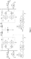
- Figure 4 is a schematic structural diagram of a typical HVDC system according to the present disclosure.
- FIG. 4 shows a schematic diagram of a typical HVDC system, which includes three parts: a rectifier side, an inverter side and a DC line.
- the rectifier side has a similar structure to the inverter side, and includes: an alternative current (AC) power grid, a converter transformer, a converter valve, an AC filter and a control system.
- the AC power grid is a Thevenin equivalent circuit, including an AC voltage source Vac, an internal resistor Rs and an internal inductor Ls that are connected in series.
- the converter transformer includes two converter transformers T1 and T2.
- the AC filter includes a capacitor, an inductor and a resistor that are connected in series or in parallel.
- the rectifier side of the control system is controlled by a constant current PI controller, and the inverter side is controlled by a constant voltage PI controller.
- the DC line shown in Figure 4 is a T-shaped circuit, and may be equivalent to a cascaded ⁇ -shaped circuit according to the length of the line.
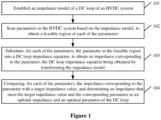
- Figure 1 is a flow chart of a method for determining a DC loop impedance according to a first method embodiment of the present disclosure.
- the method for determining a DC loop impedance according to this embodiment includes the following steps 101 to 104.
- step 101 an impedance model of a DC loop of an HVDC system is established.
- initialization is performed before establishing the impedance model.
- the initialization includes determining an input matrix according to the structure of the HVDC system and initializing relevant parameters.
- the method of establishing the impedance model for the DC loop of the HVDC system includes: establishing a state space equation associated with a primary system and a secondary control system of the HVDC system based on a structure of the HVDC system, where a small-signal model for a thyristor converter valve is established by using a switching function method, the delay effect of the switching period during 12-pulse operation of the thyristor in a triggering control operation is approximated by using Taylor expansion approximation or Pade approximation may be used to simulate the above delay effect.
- the PI controller, measurement delay, and controller delay, etc. in the control system are taken into consideration, where the measurement delay and the controller delay are simulated by using first-order Taylor expansion approximation or Pade approximation.
- step 102 parameters in the HVDC system are scanned based on the impedance model, to obtain a feasible region of each of the parameters.
- all key parameters of the HVDC system are scanned by using the state space equation in step 101, and the feasible region of each of the key parameters is determined by using an eigenvalue method or impedance analysis method.
- the feasible regions are used as value ranges of respective parameters in subsequent DC loop impedance optimization.
- each of the parameters in the feasible region is substituted into a DC loop impedance equation, to obtain an impedance corresponding to the parameter.
- the DC loop impedance equation is obtained by transforming the impedance model.
- step 103 the DC loop impedance corresponding to each parameter is calculated by substituting each parameter in the feasible region obtained in step 102 into the DC loop impedance equation obtained by transforming the state space equation obtained in step S101.
- s is a Laplacian operator
- A is the state matrix of the HVDC system
- B is the input matrix of the HVDC system.
- step 104 the impedance corresponding to each of the parameters is compared with a target impedance value, and an impedance that meet the target impedance value and the corresponding parameter are determined as an optimal impedance and an optimal parameter of the DC loop.
- the obtained DC loop impedance is compared with a design target (a target impedance value) requirement of the optimization, the impedance that meet the design requirement and the corresponding parameter are retained, and an impedance that do not meet the requirement is eliminated, to obtain the DC system parameter and the DC loop impedance that meet the design requirement.
- a design target a target impedance value
- a method for determining a DC loop impedance is provided according to this embodiment.
- an analytical calculation model of the DC loop impedance of the HVDC system is established, the feasible region of each of the parameters of the HVDC system is obtained based on the model, then the system parameter is selected in the feasible region by using an automatic optimization design method, and the system parameter and the optimal DC loop harmonic impedance that meet the target impedance value are outputted.
- This method can significantly improve the accuracy and efficiency of the DC loop impedance design of HVDC projects, avoid resonance in the DC system, and improve the stable operation of the power grid, so as to solve the technical problems of low efficiency and poor accuracy of existing DC loop impedance design methods.
- the method for determining a DC loop impedance according to the first method embodiment of the present disclosure is described above. In the following, a method for determining a DC loop impedance according to a second method embodiment of the present disclosure is introduced.
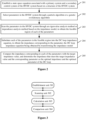
- Figure 2 is a flow chart of a method for determining a DC loop impedance according to another embodiment of the present disclosure.
- the method for determining a DC loop impedance includes the following steps 201 to 205.
- Step 201 a state space equation associated with a primary system and a secondary control system of the HVDC system is established based on a structure of the HVDC system.
- Step 201 in this embodiment is similar to step 101 in the above embodiment. Reference may be made to the description of step 101 for detailed description, which will not be repeated here.
- step 202 parameters in the HVDC system are selected through a particle algorithm or a genetic evolutionary algorithm.
- the goal of the optimization may be set according to actual requirements of the HVDC transmission system.
- the impedance of the DC link in the sensitive frequency range needs to be as large as possible.
- the minimum DC impedance Zdcmin within the frequency range may be extracted, minimum DC loop impedances Zdcmins corresponding to different parameters of the HVDC transmission system are compared with each other, and the maximum one of the Zdcmins may be determined as the goal of system optimization.
- the DC link impedance of the DC system in the sensitive frequency range that is obtained through this optimization goal has the maximum impedance minimum point, such that the harmonic current is minimum even if resonance occurs at this frequency.
- a restrictive goal may be additionally set: for example, all impedances in the sensitive frequency range are greater than Zdc0 (if less than Zdc0, when resonance occurs at this frequency, the resonant current is large, which will endanger equipment safety).
- the system parameter range and DC impedance that are selected through this optimization method and that meet the requirements can ensure that the system does not have the risk of resonance under all working conditions. Then, further optimization may be performed based on the design goals required by the dynamic characteristics, to meet more system requirements.
- Figure 5 is a diagram showing an initial impedance spectrum of a DC loop impedance at an output of a rectifier side of an HVDC transmission system according to the present disclosure.
- the curve in Figure 5 is a spectrum of an impedance calculated by using the method according to the present disclosure, where each circular point represents an impedance at a frequency point calculated by PSCAD simulation. It can be known from Figure 5 that each circular point is on the impedance spectrum curve calculated by using the method of the present disclosure, which means that the impedance calculated by the method of present disclosure has high accuracy.
- step 203 the parameters in the HVDC system are scanned through an eigenvalue analysis method or impendence analysis method based on the impedance model, to obtain the feasible region of each of the parameters.
- the impedance curve has low impedance value near 50Hz and 100Hz, and the two frequency points are more sensitive and resonance is prone to occur at the two frequency points. Therefore, the impedance near 50Hz and 100Hz may be optimized. The optimization process is described below.
- the first step is to perform feasible region solving of the system parameters.
- rectifier side constant current controller parameters Kpr and Kir are used as the system parameters to be optimized.
- the feasible region solving of Kpr and Kir is performed by solving the state matrix A by using the eigenvalue analysis method.
- the feasible regions of Kpr and Kir that make the system stable may be obtained.
- the lower left half area surrounded by the curve is the feasible regions of the system parameters, where curve 1 represents Kpr and curve 2 represents Kir.
- the second step is DC impedance optimization.
- the optimization goal is determined.
- the minimum DC impedance Zdcmin between 50Hz plus or minus 5Hz and 100Hz plus or minus 5Hz being the highest is determined as the optimization goal, that is, it is to ensure that the minimum DC impedance after optimization in the selected (45Hz, 55Hz) &&(95Hz, 105Hz) frequency band is greater than all other feasible minimum DC impedance, such that the resonance current in this frequency band is also the smallest and has the smallest impact on the system.
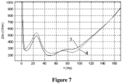
- the optimized impedance curve is shown in Figure 7 .
- Curve 4 is the optimized impedance curve, and curve 3 is the initial impedance curve. It can be seen that in the selected sensitive frequency band, the lowest point of curve 4 is above curve 3, which represents better resistance to DC resonance.
- the method of this embodiment can achieve efficient optimization of the DC loop impedance of the HVDC system, adjust the system parameters that need to be optimized according to actual needs, and set different optimization goals, so that the DC loop impedance of the HVDC system meets different technical requirements.
- This method is efficient and reliable, and does not require repeated simulation calculations of the HVDC system through electromagnetic transient simulation or other software, and does not require designers with rich engineering experience to manually adjust the system parameters iteratively, thereby saving time and manpower, and improving the design efficiency and accuracy of the DC loop impedance of the HVDC system.
- each of the parameters in the feasible region is substituted into the DC loop impedance equation, to obtain the impedance corresponding to the parameter.
- the DC loop impedance equation is obtained by transforming the impedance model.
- Step 204 in this embodiment is the same as step 103 in the above embodiment. Reference may be made the description of step 103 for detailed description, which will not be repeated here.
- step 205 the impedance corresponding to each of the parameters is compared with the target impedance value, and the impedance that meet the target impedance value and the corresponding parameter are determined as the optimal impedance and the optimal parameter of the DC loop.
- Step 205 in this embodiment is the same as step 104 in the above embodiment. Reference may be made the description of step 104 for detailed description, which will not be repeated here.
- the DC loop impedance does not need to be designed through electromagnetic transient simulation such as PSCAD, but is directly calculated through mathematical models, eliminating the lengthy modeling and simulation time required by electromagnetic transient software, and improving the calculation efficiency.
- the method of the present disclosure is to perform a global solution within the feasible regions of the system parameters. The optimal system parameters and DC loop impedance are obtained while meeting the optimization goals under the premise of system stability, avoiding insufficient consideration or insufficient optimization in manual iterative design. Therefore, the obtained DC loop impedance has higher accuracy.
- the present disclosure provides parametric analytical optimization design of the DC loop impedance according to different optimization design goals, and the optimization process can be performed automatically through computers, without the need for professional designers to repeatedly adjust and iterate system parameters, saving manpower and time, thus solving the problem of low efficiency and low accuracy of existing DC loop impedance design methods.
- the method for determining a DC loop impedance according to the second method embodiment of the present disclosure is described above.
- a system for determining a DC loop impedance according to an embodiment of the present disclosure is introduced.
- Figure 3 is a schematic structural diagram of a system for determining a DC loop impedance according to an embodiment of the present disclosure.
- the system for determining a DC loop impedance includes an establishment unit 301, a scanning unit 302, a calculation unit 303 and a comparison unit 304.
- the establishment unit 301 is configured to establish an impedance model for a DC loop of an HVDC system.
- the scanning unit 302 is configured to scan parameters in the HVDC system based on the impedance model, to obtain a feasible region of each of the parameters.
- the calculation unit 303 is configured to, for each of the parameters, substitute the parameter in the feasible region into a DC loop impedance equation, to obtain an impedance corresponding to the parameter, the DC loop impedance equation being obtained by transforming the impedance model.
- the comparison unit 304 is configured to, for each of the parameters, compare the impedance corresponding to the parameter with a target impedance value, and determine the impedance that meets the target impedance value and the parameter corresponding to the impedance as an optimal impedance and an optimal parameter of the DC loop.
- a system for determining a DC loop impedance is provided according to this embodiment.
- an analytical calculation model of the DC loop impedance of the HVDC system is established, the feasible region of each of the parameters of the HVDC system is obtained based on the model, then the system parameter is selected in the feasible region by using an automatic optimization design method, and the system parameter and the optimal DC loop harmonic impedance that meet the target impedance value are outputted.
- This method can significantly improve the accuracy and efficiency of the DC loop impedance design of HVDC projects, avoid resonance in the DC system, and improve the stable operation of the power grid, so as to solve the technical problems of low efficiency and poor accuracy of existing DC loop impedance design methods.
- the term "at least one” refers to a quantity equal to one or more
- the term “multiple” refers to a quantity equal to two or more.
- the term “and/or” is used to describe an association relationship between objects, and indicates three possible relationships. For example, “A and/or B” may indicate a case that there is only A, a case that there is only B, and a case that there are both A and B. In each case, a quantity of A may be one or more, and a quantity of B may be one or more.
- the symbol “/” generally indicates that a former object and a latter object are associated by an "or” relationship.
- At least one of or a similar expression refers to "any combination of", including any combination consisting of a single item or multiple items.
- at least one of a, b, or c may indicate: a, b, c, "a and b", “a and c", “b and c", or "a, b, and c", where a, b, and c may be singular or plural.
- the disclosed system, apparatus, and method may be implemented in other manners.
- the described apparatus embodiment is merely exemplary.
- the unit division is merely a logical function division and may be other division during actual implementation.
- multiple units or components may be combined or integrated into another system, or some features may be ignored or not performed.
- the displayed or discussed mutual couplings or direct couplings or communication connections may be implemented by using some interfaces.
- the indirect couplings or communication connections between the apparatuses or units may be implemented in electric, mechanical, or other forms.
- the above unit described as a separate component may be or may be not separated physically.
- the component displayed as a unit may be or may be not a physical unit, that is, may be located at one place or may be distributed on multiple network units. Some or all of the units may be selected according to actual needs to achieve the objectives of the solutions of the embodiments.
- functional units in the embodiments of the present disclosure may be integrated into one processing unit, or each of the units may exist alone physically, or two or more units may be integrated into one unit.
- the integrated units may be implemented in a form of hardware or in a form of a software functional unit.
- the integrated unit When the integrated unit is implemented in the form of a software functional unit and sold or used as an independent product, the integrated unit may be stored in a computer-readable storage medium.
- the technical solution of the present disclosure is essentially or part of the technical solution that make contribution to the prior art or all or part of the technical solution may be embodied in the form of a software product, and the computer software product is stored in a storage medium, including several instructions for enabling a computer device (which may be a personal computer, a server, or a network device, etc.) to execute all or part of the steps of the method described in the various embodiments of the present disclosure.
- the above-described storage medium includes: a USB disk, a removable hard disk, a read-only memory (ROM), a random access memory (RAM), a diskette, an optical disc and various media that can store program codes.
Landscapes
- Engineering & Computer Science (AREA)
- Physics & Mathematics (AREA)
- Theoretical Computer Science (AREA)
- Computer Hardware Design (AREA)
- Evolutionary Computation (AREA)
- General Physics & Mathematics (AREA)
- General Engineering & Computer Science (AREA)
- Geometry (AREA)
- Biophysics (AREA)
- Health & Medical Sciences (AREA)
- Life Sciences & Earth Sciences (AREA)
- Software Systems (AREA)
- Artificial Intelligence (AREA)
- General Health & Medical Sciences (AREA)
- Mathematical Physics (AREA)
- Biomedical Technology (AREA)
- Evolutionary Biology (AREA)
- Computational Linguistics (AREA)
- Data Mining & Analysis (AREA)
- Bioinformatics & Computational Biology (AREA)
- Molecular Biology (AREA)
- Computing Systems (AREA)
- Bioinformatics & Cheminformatics (AREA)
- Computer Networks & Wireless Communication (AREA)
- Medical Informatics (AREA)
- Computer Vision & Pattern Recognition (AREA)
- Physiology (AREA)
- Genetics & Genomics (AREA)
- Microelectronics & Electronic Packaging (AREA)
- Supply And Distribution Of Alternating Current (AREA)
- Feedback Control In General (AREA)
- Design And Manufacture Of Integrated Circuits (AREA)
Applications Claiming Priority (2)
| Application Number | Priority Date | Filing Date | Title |
|---|---|---|---|
| CN202110517868.9A CN113111623A (zh) | 2021-05-12 | 2021-05-12 | 一种直流回路阻抗的设计方法及系统 |
| PCT/CN2021/117926 WO2022237022A1 (zh) | 2021-05-12 | 2021-09-13 | 一种直流回路阻抗的设计方法及系统 |
Publications (3)
| Publication Number | Publication Date |
|---|---|
| EP4332821A1 true EP4332821A1 (de) | 2024-03-06 |
| EP4332821A8 EP4332821A8 (de) | 2024-05-08 |
| EP4332821A4 EP4332821A4 (de) | 2025-03-26 |
Family
ID=76722420
Family Applications (1)
| Application Number | Title | Priority Date | Filing Date |
|---|---|---|---|
| EP21941589.0A Pending EP4332821A4 (de) | 2021-05-12 | 2021-09-13 | Entwurfsverfahren und -system für gleichstromschleifenimpedanz |
Country Status (4)
| Country | Link |
|---|---|
| US (1) | US20240362388A1 (de) |
| EP (1) | EP4332821A4 (de) |
| CN (1) | CN113111623A (de) |
| WO (1) | WO2022237022A1 (de) |
Cited By (1)
| Publication number | Priority date | Publication date | Assignee | Title |
|---|---|---|---|---|
| CN121173118A (zh) * | 2025-11-20 | 2025-12-19 | 深圳市德兰明海新能源股份有限公司 | 并网逆变器的直流分量抑制方法、逆变器及存储介质 |
Families Citing this family (2)
| Publication number | Priority date | Publication date | Assignee | Title |
|---|---|---|---|---|
| CN113111623A (zh) * | 2021-05-12 | 2021-07-13 | 南方电网科学研究院有限责任公司 | 一种直流回路阻抗的设计方法及系统 |
| JP2024065762A (ja) * | 2022-10-31 | 2024-05-15 | 住友電気工業株式会社 | 算出プログラムおよび算出方法 |
Family Cites Families (8)
| Publication number | Priority date | Publication date | Assignee | Title |
|---|---|---|---|---|
| CN103427433B (zh) * | 2013-08-12 | 2015-06-24 | 浙江大学 | 一种混合双极直流输电系统直流回路阻抗的计算方法 |
| CN104570065B (zh) * | 2013-10-09 | 2017-05-03 | 中国石油化工股份有限公司 | 一种利用地震波阻抗定量反演孔隙度的方法 |
| WO2019002626A1 (de) * | 2017-06-30 | 2019-01-03 | Holst Detlef | Verfahren zur automatisierten ermittlung von strompfaden oder stromkreisen |
| CN107688722B (zh) * | 2017-09-27 | 2020-03-10 | 清华大学 | 电压源型变流器的导纳模型和阻抗模型获取方法及装置 |
| CN110401231B (zh) * | 2019-07-25 | 2023-01-03 | 东北大学 | 多端口能源路由器自-互-群多层次稳定辨识与回稳方法 |
| CN112364586B (zh) * | 2020-11-11 | 2024-05-14 | 南方电网科学研究院有限责任公司 | 直流换流器的直流回路阻抗计算方法、装置和计算机设备 |
| CN112231935B (zh) * | 2020-11-11 | 2024-05-31 | 南方电网科学研究院有限责任公司 | 换流器的直流回路谐波阻抗计算方法、装置和计算机设备 |
| CN113111623A (zh) * | 2021-05-12 | 2021-07-13 | 南方电网科学研究院有限责任公司 | 一种直流回路阻抗的设计方法及系统 |
-
2021
- 2021-05-12 CN CN202110517868.9A patent/CN113111623A/zh active Pending
- 2021-09-13 US US18/560,100 patent/US20240362388A1/en active Pending
- 2021-09-13 EP EP21941589.0A patent/EP4332821A4/de active Pending
- 2021-09-13 WO PCT/CN2021/117926 patent/WO2022237022A1/zh not_active Ceased
Cited By (1)
| Publication number | Priority date | Publication date | Assignee | Title |
|---|---|---|---|---|
| CN121173118A (zh) * | 2025-11-20 | 2025-12-19 | 深圳市德兰明海新能源股份有限公司 | 并网逆变器的直流分量抑制方法、逆变器及存储介质 |
Also Published As
| Publication number | Publication date |
|---|---|
| EP4332821A4 (de) | 2025-03-26 |
| EP4332821A8 (de) | 2024-05-08 |
| CN113111623A (zh) | 2021-07-13 |
| WO2022237022A1 (zh) | 2022-11-17 |
| US20240362388A1 (en) | 2024-10-31 |
Similar Documents
| Publication | Publication Date | Title |
|---|---|---|
| EP4332821A1 (de) | Entwurfsverfahren und -system für gleichstromschleifenimpedanz | |
| Khan et al. | Implementation of Distributed Generation (IDG) algorithm for performance enhancement of distribution feeder under extreme load growth | |
| JP6272396B2 (ja) | 高圧直流送電システムの複同調フィルタの設計方法 | |
| CN115579967B (zh) | 一种大电网交直流多断面的功率调整方法及系统 | |
| CN109038604B (zh) | 一种statcom接入受端弱交流系统的分析方法 | |
| CN120357463B (zh) | 一种面向能量互济的配电台区柔性互联组群规划方法 | |
| CN103279656A (zh) | 基于潮流计算的配电网最大供电能力计算方法 | |
| CN110783913A (zh) | 基于群的计及预想事故集最佳电网拓扑在线优化方法 | |
| CN106655202A (zh) | 一种基于可中断负荷的多目标过载辅助决策方法 | |
| JP2020527010A (ja) | 交流部に電力を管理するためのモジュールを備える変換器 | |
| CN113241761B (zh) | 一种电网稳定控制线性需切机量的定值整定方法及系统 | |
| Silva et al. | Performance of predictive control applied to active power filter | |
| CN110071499B (zh) | 一种快速判断配电网安全合环的方法和系统 | |
| EP4461954A1 (de) | Verfahren zur installation und steuerung einer offshore-windkraftanlage | |
| CN112165097A (zh) | 确定感应电动机贡献短路电流的等效比例的方法及系统 | |
| CN102570460A (zh) | 一种计算电气化铁路的谐波和负序电流的方法 | |
| CN111813093B (zh) | 一种配电台区电压协调控制器的检测系统 | |
| Gole et al. | Electromagnetic transients simulation as an objective function evaluator for optimization of power system performance | |
| CN110474355B (zh) | 一种用于优化可移动储能式充电装置容量配置的方法及系统 | |
| Lopez-Fernandez et al. | A High frequency power transformers model for network studies and TDSF monitoring | |
| Crownshaw et al. | Determination of distributed generation hosting capacity in low-voltage networks and industry applications | |
| Turkovskyi et al. | The simulation and analysis of the probabilistic characteristics of schemes for power supply of electric arc furnaces in non-symmetric modes | |
| Darvishi et al. | Fuzzy multi-objective technique integrated with differential evolution method to optimise power factor and total harmonic distortion | |
| CN104732101A (zh) | 电网调度操作中系统总有功失负荷值确定方法和系统 | |
| CN120764494B (zh) | 一种基于实体关系抽取的电力文档数据生成方法和装置 |
Legal Events
| Date | Code | Title | Description |
|---|---|---|---|
| STAA | Information on the status of an ep patent application or granted ep patent |
Free format text: STATUS: THE INTERNATIONAL PUBLICATION HAS BEEN MADE |
|
| PUAI | Public reference made under article 153(3) epc to a published international application that has entered the european phase |
Free format text: ORIGINAL CODE: 0009012 |
|
| STAA | Information on the status of an ep patent application or granted ep patent |
Free format text: STATUS: REQUEST FOR EXAMINATION WAS MADE |
|
| 17P | Request for examination filed |
Effective date: 20231127 |
|
| AK | Designated contracting states |
Kind code of ref document: A1 Designated state(s): AL AT BE BG CH CY CZ DE DK EE ES FI FR GB GR HR HU IE IS IT LI LT LU LV MC MK MT NL NO PL PT RO RS SE SI SK SM TR |
|
| RAP3 | Party data changed (applicant data changed or rights of an application transferred) |
Owner name: CHINA SOUTHERN POWER GRID Owner name: ELECTRIC POWER RESEARCH INSTITUTE. CHINA SOUTHERN POWER GRID |
|
| DAV | Request for validation of the european patent (deleted) | ||
| DAX | Request for extension of the european patent (deleted) | ||
| A4 | Supplementary search report drawn up and despatched |
Effective date: 20250221 |
|
| RIC1 | Information provided on ipc code assigned before grant |
Ipc: G06N 3/006 20230101ALN20250217BHEP Ipc: G06N 3/126 20230101ALN20250217BHEP Ipc: G06F 111/10 20200101ALN20250217BHEP Ipc: G06F 111/06 20200101ALN20250217BHEP Ipc: G06F 30/367 20200101ALI20250217BHEP Ipc: G06F 30/27 20200101ALI20250217BHEP Ipc: G06N 3/00 20230101ALI20250217BHEP Ipc: G06F 30/398 20200101ALI20250217BHEP Ipc: G06F 30/3947 20200101AFI20250217BHEP |
|
| STAA | Information on the status of an ep patent application or granted ep patent |
Free format text: STATUS: EXAMINATION IS IN PROGRESS |
|
| 17Q | First examination report despatched |
Effective date: 20251223 |