EP4333083A1 - Cellule solaire à hétérojonction et son procédé de fabrication - Google Patents
Cellule solaire à hétérojonction et son procédé de fabrication Download PDFInfo
- Publication number
- EP4333083A1 EP4333083A1 EP23194562.7A EP23194562A EP4333083A1 EP 4333083 A1 EP4333083 A1 EP 4333083A1 EP 23194562 A EP23194562 A EP 23194562A EP 4333083 A1 EP4333083 A1 EP 4333083A1
- Authority
- EP
- European Patent Office
- Prior art keywords
- layer
- oxygen
- microcrystalline
- type
- solar cell
- Prior art date
- Legal status (The legal status is an assumption and is not a legal conclusion. Google has not performed a legal analysis and makes no representation as to the accuracy of the status listed.)
- Granted
Links
Images




Classifications
-
- H—ELECTRICITY
- H10—SEMICONDUCTOR DEVICES; ELECTRIC SOLID-STATE DEVICES NOT OTHERWISE PROVIDED FOR
- H10F—INORGANIC SEMICONDUCTOR DEVICES SENSITIVE TO INFRARED RADIATION, LIGHT, ELECTROMAGNETIC RADIATION OF SHORTER WAVELENGTH OR CORPUSCULAR RADIATION
- H10F10/00—Individual photovoltaic cells, e.g. solar cells
- H10F10/10—Individual photovoltaic cells, e.g. solar cells having potential barriers
- H10F10/16—Photovoltaic cells having only PN heterojunction potential barriers
- H10F10/164—Photovoltaic cells having only PN heterojunction potential barriers comprising heterojunctions with Group IV materials, e.g. ITO/Si or GaAs/SiGe photovoltaic cells
- H10F10/165—Photovoltaic cells having only PN heterojunction potential barriers comprising heterojunctions with Group IV materials, e.g. ITO/Si or GaAs/SiGe photovoltaic cells the heterojunctions being Group IV-IV heterojunctions, e.g. Si/Ge, SiGe/Si or Si/SiC photovoltaic cells
- H10F10/166—Photovoltaic cells having only PN heterojunction potential barriers comprising heterojunctions with Group IV materials, e.g. ITO/Si or GaAs/SiGe photovoltaic cells the heterojunctions being Group IV-IV heterojunctions, e.g. Si/Ge, SiGe/Si or Si/SiC photovoltaic cells the Group IV-IV heterojunctions being heterojunctions of crystalline and amorphous materials, e.g. silicon heterojunction [SHJ] photovoltaic cells
-
- H—ELECTRICITY
- H10—SEMICONDUCTOR DEVICES; ELECTRIC SOLID-STATE DEVICES NOT OTHERWISE PROVIDED FOR
- H10F—INORGANIC SEMICONDUCTOR DEVICES SENSITIVE TO INFRARED RADIATION, LIGHT, ELECTROMAGNETIC RADIATION OF SHORTER WAVELENGTH OR CORPUSCULAR RADIATION
- H10F10/00—Individual photovoltaic cells, e.g. solar cells
- H10F10/10—Individual photovoltaic cells, e.g. solar cells having potential barriers
- H10F10/16—Photovoltaic cells having only PN heterojunction potential barriers
- H10F10/164—Photovoltaic cells having only PN heterojunction potential barriers comprising heterojunctions with Group IV materials, e.g. ITO/Si or GaAs/SiGe photovoltaic cells
- H10F10/165—Photovoltaic cells having only PN heterojunction potential barriers comprising heterojunctions with Group IV materials, e.g. ITO/Si or GaAs/SiGe photovoltaic cells the heterojunctions being Group IV-IV heterojunctions, e.g. Si/Ge, SiGe/Si or Si/SiC photovoltaic cells
-
- H—ELECTRICITY
- H10—SEMICONDUCTOR DEVICES; ELECTRIC SOLID-STATE DEVICES NOT OTHERWISE PROVIDED FOR
- H10F—INORGANIC SEMICONDUCTOR DEVICES SENSITIVE TO INFRARED RADIATION, LIGHT, ELECTROMAGNETIC RADIATION OF SHORTER WAVELENGTH OR CORPUSCULAR RADIATION
- H10F71/00—Manufacture or treatment of devices covered by this subclass
- H10F71/121—The active layers comprising only Group IV materials
-
- H—ELECTRICITY
- H10—SEMICONDUCTOR DEVICES; ELECTRIC SOLID-STATE DEVICES NOT OTHERWISE PROVIDED FOR
- H10F—INORGANIC SEMICONDUCTOR DEVICES SENSITIVE TO INFRARED RADIATION, LIGHT, ELECTROMAGNETIC RADIATION OF SHORTER WAVELENGTH OR CORPUSCULAR RADIATION
- H10F71/00—Manufacture or treatment of devices covered by this subclass
- H10F71/121—The active layers comprising only Group IV materials
- H10F71/1224—The active layers comprising only Group IV materials comprising microcrystalline silicon
-
- H—ELECTRICITY
- H10—SEMICONDUCTOR DEVICES; ELECTRIC SOLID-STATE DEVICES NOT OTHERWISE PROVIDED FOR
- H10F—INORGANIC SEMICONDUCTOR DEVICES SENSITIVE TO INFRARED RADIATION, LIGHT, ELECTROMAGNETIC RADIATION OF SHORTER WAVELENGTH OR CORPUSCULAR RADIATION
- H10F71/00—Manufacture or treatment of devices covered by this subclass
- H10F71/128—Annealing
-
- H—ELECTRICITY
- H10—SEMICONDUCTOR DEVICES; ELECTRIC SOLID-STATE DEVICES NOT OTHERWISE PROVIDED FOR
- H10F—INORGANIC SEMICONDUCTOR DEVICES SENSITIVE TO INFRARED RADIATION, LIGHT, ELECTROMAGNETIC RADIATION OF SHORTER WAVELENGTH OR CORPUSCULAR RADIATION
- H10F77/00—Constructional details of devices covered by this subclass
- H10F77/70—Surface textures, e.g. pyramid structures
- H10F77/703—Surface textures, e.g. pyramid structures of the semiconductor bodies, e.g. textured active layers
-
- Y—GENERAL TAGGING OF NEW TECHNOLOGICAL DEVELOPMENTS; GENERAL TAGGING OF CROSS-SECTIONAL TECHNOLOGIES SPANNING OVER SEVERAL SECTIONS OF THE IPC; TECHNICAL SUBJECTS COVERED BY FORMER USPC CROSS-REFERENCE ART COLLECTIONS [XRACs] AND DIGESTS
- Y02—TECHNOLOGIES OR APPLICATIONS FOR MITIGATION OR ADAPTATION AGAINST CLIMATE CHANGE
- Y02P—CLIMATE CHANGE MITIGATION TECHNOLOGIES IN THE PRODUCTION OR PROCESSING OF GOODS
- Y02P70/00—Climate change mitigation technologies in the production process for final industrial or consumer products
- Y02P70/50—Manufacturing or production processes characterised by the final manufactured product
Definitions
- the present disclosure belongs to the technical field of solar cells, and in particular to a heterojunction solar cell and a manufacturing method thereof.
- the heterojunction solar cell With a high conversion efficiency, low process temperature, high stability and low degradation rate, the heterojunction solar cell has been increasingly popular in the photovoltaic industry and is envisioned as a future development trend for high-conversion-efficiency solar cells.
- Heterojunction technology has great development potential due to its simple process, high conversion efficiency, high comprehensive power output, and far lower degradation rate than passivated emitter and rear cell (PERC) technology.
- the plate-type plasma-enhanced chemical vapor deposition (PECVD) coating equipment used for amorphous silicon or microcrystalline silicon is costly.
- the heterojunction technology is not advantageous over the PERC technology in terms of the comprehensive equipment cost. It is desirable to improve production technology to further reduce the equipment investment, thereby making comprehensive investment competitive in the markets.
- An objective of the present disclosure is to provide a manufacturing method of a heterojunction solar cell. With a simple process, the manufacturing method keeps not only the high conductivity and low equipment investment of an N-type polysilicon layer, but also the desirable passivation and high open-circuit voltage of a heterojunction technology.
- the tunnel oxide passivated contact (TOPCON) technology formed by a tunnel oxide layer and an N-type polysilicon layer on a back surface of the heterojunction solar cell has a good passivation effect and a desirable conductivity.
- AP-type microcrystalline laminated layer is provided on a front surface of the heterojunction solar cell.
- An oxygen-containing microcrystalline layer enhances an electrical potential barrier, while expanding an optical band gap. This ensures an open-circuit voltage of the cell, and improves a fill factor of the cell.
- a manufacturing method of a heterojunction solar cell includes the following steps:
- a heterojunction solar cell includes a first electrode, a first conductive film layer, a P-type microcrystalline laminated layer, an intrinsic film layer, the semiconductor substrate, the tunnel oxide layer, an N-type semiconductor film layer, a second conductive film layer, and a second electrode that are sequentially stacked from a light-facing surface to a backlight surface, where the P-type microcrystalline laminated layer includes at least one oxygen-containing microcrystalline layer and at least one oxygen-free microcrystalline layer.
- 1 silicon wafer
- 2 tunnel oxide layer
- 3 first intrinsic polysilicon layer
- 4 N-type polysilicon layer
- 5 PSG layer
- 6 silicon nitride protective layer
- 7 second intrinsic amorphous silicon layer
- 8 P-type oxygen-doped microcrystalline silicon layer
- 81 first oxygen-free microcrystalline layer
- 82 oxygen-containing microcrystalline layer
- 83 second oxygen-free microcrystalline layer
- 9 transparent conductive layer
- 10 metal grid electrode.
- a manufacturing method of a heterojunction solar cell includes the following steps:
- the manufacturing method further includes the following steps:
- Step A polishing and cleaning are further performed. Specifically, the semiconductor substrate is polished for 1-15 min with an alkaline solution at 65-90°C to remove a thickness of 1-20 ⁇ m, and cleaned with a weak alkaline solution and an acidic solution.
- Step A specifically includes: The tunnel oxide layer is formed on the surface of the semiconductor substrate by nitric acid oxidation, ozone oxidation, vacuum plasma-assisted oxidation or thermal oxidation.
- the thermal oxidation is to charge oxygen for oxidation, an oxygen and nitrogen mixture for oxidation or aerial oxygen for oxidation at 550-650°C.
- Step B specifically includes: A first intrinsic polysilicon layer is formed on the tunnel oxide layer. Phosphorus doping is performed on the first intrinsic polysilicon layer by diffusion annealing to form the N-type polysilicon layer and a PSG layer. The PSG layer is removed with a fluorine-containing acidic solution. Or, a phosphorus source is introduced by low-pressure CVD (LPCVD) for in-situ doped growth, thereby forming the N-type polysilicon layer.
- LPCVD low-pressure CVD
- the first intrinsic polysilicon layer is grown by the LPCVD, or obtained by preparing an amorphous silicon layer and a microcrystalline silicon layer with PECVD and then performing high-temperature annealing, or obtained by sputtering a silicon target material through a physical vapor deposition (PVD) to prepare a silicon thin film and then performing high-temperature annealing.
- PVD physical vapor deposition
- Step A and Step B specifically include:
- the semiconductor substrate is put into a tubular LPCVD device, and thermally oxidized for 30 min at 550-650°C to form the tunnel oxide layer.
- Vacuumization is performed, and a reactant gas is charged to grow the first intrinsic polysilicon layer at 550-650°C and 5-10,000 Pa, the grown first intrinsic polysilicon layer having a thickness of 20-300 nm.
- the phosphorus doping is performed on the first intrinsic polysilicon layer by the diffusion annealing to form the N-type polysilicon layer and the PSG layer.
- the PSG layer is removed with the fluorine-containing acidic solution.
- the diffusion annealing in Step B is to perform boron doping on the first intrinsic polysilicon layer at 780-950°C. Upon diffusion, a sheet resistance is 20-200 S2/square.
- Step C specifically includes: At least one of silicon nitride, silicon oxynitride and silicon oxide is deposited on the N-type polysilicon layer by plasma CVD (PCVD) or high-temperature CVD to form the mask layer.
- PCVD plasma CVD
- CVD high-temperature CVD
- the mask layer has a thickness of 30-150 nm.
- Step D specifically includes: A pyramid texture is formed on the second main surface of the semiconductor substrate through the texturing and the cleaning, and the mask layer is removed with a fluorine-containing acidic solution.
- the tunnel oxide layer has a thickness of 1-2 nm.
- the N-type polysilicon layer has a thickness of 20-300 nm.
- the P-type oxygen-doped microcrystalline silicon layer has a thickness of 5-25 nm.
- Step F specifically includes: The P-type oxygen-doped microcrystalline silicon layer laminated by at least one oxygen-containing microcrystalline layer and at least one oxygen-free microcrystalline layer is formed by PECVD or hot-wire CVD.
- a first oxygen-free microcrystalline layer, the oxygen-containing microcrystalline layer, and a second oxygen-free microcrystalline layer are sequentially deposited on the second intrinsic amorphous silicon layer.
- each film layer in the P-type oxygen-doped microcrystalline silicon layer is deposited by stepwise increasing a ratio of a P-type dopant gas to silane.
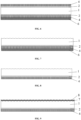
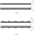
- FIG. 2 to FIG. 10 are a schematic view in a manufacturing method of a heterojunction solar cell according to an embodiment of the present disclosure.
- a manufacturing method of a heterojunction solar cell specifically includes the following steps:
- each film layer of the P-type oxygen-doped microcrystalline silicon layer is deposited by stepwise increasing a ratio of a P-type dopant gas to silane. The ratio of the P-type dopant gas to the silane is increased from 1: 10 to 1: 1.
- the above table shows a comparison of three photovoltaic cell technologies in typical electrical property, namely A: a TOPCON technology, B: a heterojunction technology, and C: related hybrid passivation technology in the present disclosure.
- a heterojunction solar cell includes the first electrode, the first conductive film layer, the P-type microcrystalline laminated layer, the intrinsic film layer, the semiconductor substrate, the tunnel oxide layer, the N-type semiconductor film layer, the second conductive film layer, and the second electrode that are sequentially stacked from a light-facing surface to a backlight surface.
- the P-type microcrystalline laminated layer includes at least one oxygen-containing microcrystalline layer and at least one oxygen-free microcrystalline layer.
- the second conductive film layer covers the N-type semiconductor film layer.
- the second electrode is provided on a surface of the second conductive film layer, thereby forming full contact between the conductive film layer and the semiconductor film layer. This prevents transverse flow of a current in the semiconductor film layer, and improves a conductivity.
- the semiconductor substrate is the monocrystalline silicon wafer.
- the pyramid texture is provided on the light-facing surface of the semiconductor substrate.
- the backlight surface of the semiconductor substrate is a chemically polished surface.
- the intrinsic film layer is a hydrogenated intrinsic amorphous silicon layer, and has a thickness of 3-12 nm.
- the P-type microcrystalline laminated layer has a thickness of 9-45 nm.
- the N-type semiconductor film layer is the N-type polysilicon layer.
- the tunnel oxide layer has a thickness of 1-2 nm.
- the N-type polysilicon layer has a thickness of 20-300 nm, and a sheet resistance of 30-200 S2/square.
- a highly doped crystalline silicon film layer is provided between the N-type semiconductor film layer and the second conductive film layer.
- the highly doped crystalline silicon film layer has a thickness of 0.3-3 nm, and a doping concentration of 1 ⁇ 10 19 -2 ⁇ 10 20 cm -3 .
- polysilicon is very likely to form a silicon oxide thin layer at a low temperature. With a thickness of about 1 nm, the silicon oxide thin layer is formed on the N-type polysilicon layer 4 to cause dramatic decrease of the conductivity.
- the highly doped crystalline silicon film layer is an N-type doped (such as phosphorous doped) polysilicon thin film, or an N-type doped microcrystalline silicon thin film, or a microcrystalline and amorphous hybrid silicon thin film, and is formed by chemical deposition or physical bombardment. With a higher N-type doping rate than the N-type semiconductor film layer and a higher disordered state than the N-type semiconductor film layer, the highly doped crystalline silicon film layer is not prone to oxidation.
- the highly doped crystalline silicon film layer is very thin, and generally has a polycrystalline state, a microcrystalline state, and a polycrystalline and microcrystalline hybrid state.
- a microcrystallization rate of the highly doped crystalline silicon film layer is controlled at 10-70%.
- the N-type doping rate of the highly doped crystalline silicon film layer is 1-5 times the N-type doping rate of the N-type semiconductor film layer.
- the P-type microcrystalline laminated layer and the N-type semiconductor film layer have a conductive doping concentration of 1 ⁇ 10 19 -2 ⁇ 10 20 cm -3 .
- the first conductive film layer and/or the second conductive film layer are a transparent conductive film layer.
- the transparent conductive film layer is one or more of an indium tin oxide (ITO) film layer, a tungsten-doped indium oxide (IWO) film layer, an indium gallium zinc oxide (IGZO) film layer, an aluminum-doped zinc oxide (AZO) film layer, a zinc-doped indium oxide (IZO) film layer, a gallium-doped zinc oxide (GZO) film layer, and a titanium-doped indium oxide (ITiO) film layer.
- ITO indium tin oxide
- IWO tungsten-doped indium oxide
- IGZO indium gallium zinc oxide
- AZO aluminum-doped zinc oxide
- IZO zinc-doped indium oxide
- GZO gallium-doped zinc oxide
- ITiO titanium-doped indium oxide
- the first conductive film layer has a thickness of 60-110 nm, and the second conductive film layer has a thickness of 15-50 nm.
- the oxygen-containing microcrystalline layer has a thickness of 5-20 nm
- the oxygen-free microcrystalline layer has a thickness of 5-20 nm.
- the P-type microcrystalline laminated layer includes the oxygen-free microcrystalline layer, the oxygen-containing microcrystalline layer, and the oxygen-free incubation layer that are sequentially stacked from the light-facing surface to the backlight surface.
- the corresponding proportion of the oxygen-free microcrystalline layer to the oxygen-containing microcrystalline layer to the oxygen-free incubation layer in thickness is (0.5-1.5): 1:(0.15-0.6).
- Each film layer in the P-type oxygen-doped microcrystalline silicon layer is deposited by stepwise increasing the ratio of the P-type dopant gas to the silane.
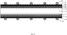
- FIG. 14 is a schematic view of a heterojunction solar cell according to an embodiment of the present disclosure.
- a heterojunction solar cell includes a first electrode, a first conductive film layer, a P-type microcrystalline laminated layer, an intrinsic film layer, a semiconductor substrate, tunnel oxide layer 2, an N-type semiconductor film layer, a second conductive film layer, and a second electrode that are sequentially stacked from a light-facing surface to a backlight surface.
- the second conductive film layer covers the N-type semiconductor film layer.
- the second electrode is provided on a surface of the second conductive film layer, thereby forming full contact between the conductive film layer and the semiconductor film layer. This prevents transverse flow of a current in the semiconductor film layer, and improves a conductivity.
- the semiconductor substrate is monocrystalline silicon wafer 1.
- a pyramid texture is provided on the light-facing surface of the semiconductor substrate.
- the backlight surface of the semiconductor substrate is a chemically polished surface.
- the intrinsic film layer is a hydrogenated intrinsic amorphous silicon layer (second intrinsic amorphous silicon layer 7), and has a thickness of 3-12 nm.
- the P-type microcrystalline laminated layer has a thickness of 9-45 nm.
- the N-type semiconductor film layer is N-type polysilicon layer 4.
- Highly doped crystalline silicon film layer 4a is provided between the N-type semiconductor film layer and the second conductive film layer.
- the first conductive film layer and the second conductive film layer are transparent conductive film layers (transparent conductive layers 9).
- the P-type microcrystalline laminated layer includes an oxygen-free microcrystalline layer (second oxygen-free microcrystalline layer 83), oxygen-containing microcrystalline layer 82, and an oxygen-free incubation layer (first oxygen-free microcrystalline layer 81) that are sequentially stacked from the light-facing surface to the backlight surface.
- second oxygen-free microcrystalline layer 83 oxygen-free microcrystalline layer
- first oxygen-free microcrystalline layer 81 oxygen-free incubation layer
- the first electrode and the second electrode are metal grid electrodes 10.
Landscapes
- Photovoltaic Devices (AREA)
- Life Sciences & Earth Sciences (AREA)
- Engineering & Computer Science (AREA)
- Sustainable Energy (AREA)
Applications Claiming Priority (2)
| Application Number | Priority Date | Filing Date | Title |
|---|---|---|---|
| CN202211061849.0A CN115132884B (zh) | 2022-09-01 | 2022-09-01 | 一种异质结太阳能电池的制作方法 |
| CN202211095468.4A CN115172481B (zh) | 2022-09-08 | 2022-09-08 | 异质结太阳能电池 |
Publications (2)
| Publication Number | Publication Date |
|---|---|
| EP4333083A1 true EP4333083A1 (fr) | 2024-03-06 |
| EP4333083B1 EP4333083B1 (fr) | 2026-04-08 |
Family
ID=87889162
Family Applications (1)
| Application Number | Title | Priority Date | Filing Date |
|---|---|---|---|
| EP23194562.7A Active EP4333083B1 (fr) | 2022-09-01 | 2023-08-31 | Procédé de fabrication d'une cellule solaire à hétérojonction |
Country Status (2)
| Country | Link |
|---|---|
| US (1) | US12342630B2 (fr) |
| EP (1) | EP4333083B1 (fr) |
Cited By (2)
| Publication number | Priority date | Publication date | Assignee | Title |
|---|---|---|---|---|
| CN118867060A (zh) * | 2024-09-26 | 2024-10-29 | 眉山琏升光伏科技有限公司 | 一种用于异质结太阳能电池高性能钝化膜及其制备方法 |
| CN119421556A (zh) * | 2024-07-26 | 2025-02-11 | 隆基绿能科技股份有限公司 | 一种太阳能电池及其制作方法、光伏组件 |
Families Citing this family (5)
| Publication number | Priority date | Publication date | Assignee | Title |
|---|---|---|---|---|
| CN118943225A (zh) * | 2023-05-10 | 2024-11-12 | 天合光能股份有限公司 | 杂化太阳能电池及光伏组件 |
| CN118073478B (zh) * | 2024-04-19 | 2024-08-13 | 金阳(泉州)新能源科技有限公司 | 一种背接触电池的制备方法及背接触电池 |
| CN118281090B (zh) * | 2024-05-24 | 2024-10-11 | 通威太阳能(安徽)有限公司 | 太阳电池及其制备方法、生产设备 |
| CN118969880B (zh) * | 2024-10-17 | 2024-12-20 | 福建金石能源有限公司 | 具有特定p型发射极的联合钝化背接触电池及制作和应用 |
| CN121262926B (zh) * | 2025-12-05 | 2026-03-17 | 福建省金石能源股份有限公司 | 一种提高钝化性能的背接触电池制作方法及其背接触电池 |
Citations (1)
| Publication number | Priority date | Publication date | Assignee | Title |
|---|---|---|---|---|
| CN114823936A (zh) * | 2022-05-18 | 2022-07-29 | 东方日升新能源股份有限公司 | 一种异质结电池及其制备方法 |
Family Cites Families (7)
| Publication number | Priority date | Publication date | Assignee | Title |
|---|---|---|---|---|
| CN111370521A (zh) * | 2018-12-26 | 2020-07-03 | 君泰创新(北京)科技有限公司 | 硅异质结太阳能电池及其发射极和发射极的制备方法 |
| CN110085699A (zh) | 2019-04-22 | 2019-08-02 | 通威太阳能(成都)有限公司 | 一种具有钝化接触结构的p型高效电池及其制作方法 |
| CN110911505B (zh) | 2019-12-19 | 2025-02-07 | 通威太阳能(眉山)有限公司 | 异质结太阳能电池片及其制造方法 |
| CN111416014B (zh) * | 2020-05-08 | 2022-03-04 | 熵熠(上海)能源科技有限公司 | 一种钝化接触背结硅异质结太阳电池及其制备方法 |
| CN114628538A (zh) | 2020-11-27 | 2022-06-14 | 福建新峰二维材料科技有限公司 | N型掺氧型微晶作为窗口层的异质结光伏电池的制备方法 |
| CN113113502B (zh) | 2021-05-11 | 2025-07-29 | 通威太阳能(成都)有限公司 | 一种异质结太阳能电池及制备方法 |
| CN113471311B (zh) * | 2021-07-06 | 2023-05-23 | 安徽华晟新能源科技有限公司 | 一种异质结电池及其制备方法 |
-
2023
- 2023-08-31 EP EP23194562.7A patent/EP4333083B1/fr active Active
- 2023-09-01 US US18/241,318 patent/US12342630B2/en active Active
Patent Citations (1)
| Publication number | Priority date | Publication date | Assignee | Title |
|---|---|---|---|---|
| CN114823936A (zh) * | 2022-05-18 | 2022-07-29 | 东方日升新能源股份有限公司 | 一种异质结电池及其制备方法 |
Non-Patent Citations (4)
| Title |
|---|
| KHELIL M ET AL: "Growth of crystalline silicon by a seed layer approach using plasma enhanced chemical vapor deposition", PHYSICA B: CONDENSED MATTER, ELSEVIER, AMSTERDAM, NL, vol. 609, 13 February 2021 (2021-02-13), XP086519142, ISSN: 0921-4526, [retrieved on 20210213], DOI: 10.1016/J.PHYSB.2021.412817 * |
| KHOKHAR MUHAMMAD QUDDAMAH ET AL: "High-efficiency hybrid solar cell with a nano-crystalline silicon oxide layer as an electron-selective contact", ENERGY CONVERSION AND MANAGEMENT, vol. 252, no. 115033, 20 November 2021 (2021-11-20), GB, pages 1 - 11, XP093116267, ISSN: 0196-8904, DOI: 10.1016/j.enconman.2021.115033 * |
| LIMODIO G ET AL: "Front and rear contact Si solar cells combining high and low thermal budget Si passivating contacts", SOLAR ENERGY MATERIALS AND SOLAR CELLS, vol. 194, 8 February 2019 (2019-02-08), pages 28 - 35, XP085643227, ISSN: 0927-0248, DOI: 10.1016/J.SOLMAT.2019.01.039 * |
| PARK HYUNJUNG ET AL: "Tunnel oxide passivating electron contacts for high-efficiency n-type silicon solar cells with amorphous silicon passivating hole contacts", PROGRESS IN PHOTOVOLTAICS: RESEARCH AND APPLICATIONS, vol. 27, no. 12, 16 October 2019 (2019-10-16), Hoboken, USA, pages 1104 - 1114, XP093116277, ISSN: 1062-7995, DOI: 10.1002/pip.3190 * |
Cited By (2)
| Publication number | Priority date | Publication date | Assignee | Title |
|---|---|---|---|---|
| CN119421556A (zh) * | 2024-07-26 | 2025-02-11 | 隆基绿能科技股份有限公司 | 一种太阳能电池及其制作方法、光伏组件 |
| CN118867060A (zh) * | 2024-09-26 | 2024-10-29 | 眉山琏升光伏科技有限公司 | 一种用于异质结太阳能电池高性能钝化膜及其制备方法 |
Also Published As
| Publication number | Publication date |
|---|---|
| EP4333083B1 (fr) | 2026-04-08 |
| US12342630B2 (en) | 2025-06-24 |
| US20240079511A1 (en) | 2024-03-07 |
Similar Documents
| Publication | Publication Date | Title |
|---|---|---|
| EP4333083A1 (fr) | Cellule solaire à hétérojonction et son procédé de fabrication | |
| EP2110859B1 (fr) | Convertisseur photoélectrique de type laminé et son procédé de fabrication | |
| CN115172481B (zh) | 异质结太阳能电池 | |
| CN115000246B (zh) | P型钝化接触电池制备方法及钝化接触电池 | |
| CN115132884B (zh) | 一种异质结太阳能电池的制作方法 | |
| CN218414591U (zh) | 太阳能电池 | |
| CN115425114B (zh) | 一种异质结太阳能电池的制造方法 | |
| US20130157404A1 (en) | Double-sided heterojunction solar cell based on thin epitaxial silicon | |
| EP4345920A1 (fr) | Batterie à contact passivé et procédé de préparation associé | |
| EP4383350A1 (fr) | Cellule solaire et son procédé de fabrication | |
| CN218513468U (zh) | 一种向光面隧穿型异质结太阳能电池 | |
| WO2023092977A1 (fr) | Procédé de préparation d'une couche d'oxyde tunnel et d'un film mince de silicium amorphe, et cellule de topcon | |
| US20100258168A1 (en) | Silicon-based dielectric stack passivation of si-epitaxial thin-film solar cells | |
| Untila et al. | ITO/SiOx/n-Si heterojunction solar cell with bifacial 16.6%/14.6% front/rear efficiency produced by ultrasonic spray pyrolysis: Effect of conditions of SiOx growth by wet-chemical oxidation | |
| AU2023343930A1 (en) | Solar cell and manufacturing method therefor | |
| CN116779693A (zh) | 一种高效异质结太阳能电池及其制作方法 | |
| JP2009038064A (ja) | 光電変換装置及びその製造方法 | |
| US20260040723A1 (en) | Photovoltaic cell, method for producing the same and photovoltaic module | |
| US8652871B2 (en) | Method for depositing an amorphous silicon film for photovoltaic devices with reduced light-induced degradation for improved stabilized performance | |
| CN118156362B (zh) | 一种带有p型隧穿结构的异质结太阳能电池的制造方法 | |
| CN211654834U (zh) | 高效p型晶体硅太阳能电池 | |
| EP4333082B1 (fr) | Procédé de fabrication d'une cellule solaire à hétérojonction | |
| CN117673201A (zh) | 一种带有p型隧穿结构的异质结太阳能电池的制备方法 | |
| CN217606831U (zh) | 一种高效异质结太阳能电池 | |
| WO2019188716A1 (fr) | Photopile et son procédé de fabrication |
Legal Events
| Date | Code | Title | Description |
|---|---|---|---|
| PUAI | Public reference made under article 153(3) epc to a published international application that has entered the european phase |
Free format text: ORIGINAL CODE: 0009012 |
|
| STAA | Information on the status of an ep patent application or granted ep patent |
Free format text: STATUS: REQUEST FOR EXAMINATION WAS MADE |
|
| 17P | Request for examination filed |
Effective date: 20230831 |
|
| AK | Designated contracting states |
Kind code of ref document: A1 Designated state(s): AL AT BE BG CH CY CZ DE DK EE ES FI FR GB GR HR HU IE IS IT LI LT LU LV MC ME MK MT NL NO PL PT RO RS SE SI SK SM TR |
|
| STAA | Information on the status of an ep patent application or granted ep patent |
Free format text: STATUS: EXAMINATION IS IN PROGRESS |
|
| 17Q | First examination report despatched |
Effective date: 20241025 |
|
| REG | Reference to a national code |
Ref country code: DE Ref legal event code: R079 Free format text: PREVIOUS MAIN CLASS: H01L0031074700 Ipc: H10F0010165000 Ref document number: 602023014779 Country of ref document: DE |
|
| GRAP | Despatch of communication of intention to grant a patent |
Free format text: ORIGINAL CODE: EPIDOSNIGR1 |
|
| STAA | Information on the status of an ep patent application or granted ep patent |
Free format text: STATUS: GRANT OF PATENT IS INTENDED |
|
| RIC1 | Information provided on ipc code assigned before grant |
Ipc: H10F 10/165 20250101AFI20251015BHEP Ipc: H10F 10/166 20250101ALI20251015BHEP Ipc: H10F 71/00 20250101ALI20251015BHEP Ipc: H10F 77/70 20250101ALI20251015BHEP |
|
| INTG | Intention to grant announced |
Effective date: 20251103 |
|
| GRAS | Grant fee paid |
Free format text: ORIGINAL CODE: EPIDOSNIGR3 |
|
| GRAA | (expected) grant |
Free format text: ORIGINAL CODE: 0009210 |
|
| STAA | Information on the status of an ep patent application or granted ep patent |
Free format text: STATUS: THE PATENT HAS BEEN GRANTED |
|
| AK | Designated contracting states |
Kind code of ref document: B1 Designated state(s): AL AT BE BG CH CY CZ DE DK EE ES FI FR GB GR HR HU IE IS IT LI LT LU LV MC ME MK MT NL NO PL PT RO RS SE SI SK SM TR |
|
| REG | Reference to a national code |
Ref country code: CH Ref legal event code: F10 Free format text: ST27 STATUS EVENT CODE: U-0-0-F10-F00 (AS PROVIDED BY THE NATIONAL OFFICE) Effective date: 20260408 Ref country code: GB Ref legal event code: FG4D |
|
| REG | Reference to a national code |
Ref country code: DE Ref legal event code: R096 Ref document number: 602023014779 Country of ref document: DE |