EP4336443B1 - Procédé et appareil de détection de défaut de surface de cellule de batterie - Google Patents
Procédé et appareil de détection de défaut de surface de cellule de batterie Download PDFInfo
- Publication number
- EP4336443B1 EP4336443B1 EP23744030.0A EP23744030A EP4336443B1 EP 4336443 B1 EP4336443 B1 EP 4336443B1 EP 23744030 A EP23744030 A EP 23744030A EP 4336443 B1 EP4336443 B1 EP 4336443B1
- Authority
- EP
- European Patent Office
- Prior art keywords
- defect
- cell
- image
- detected
- surface area
- Prior art date
- Legal status (The legal status is an assumption and is not a legal conclusion. Google has not performed a legal analysis and makes no representation as to the accuracy of the status listed.)
- Active
Links
Images



Classifications
-
- G—PHYSICS
- G06—COMPUTING OR CALCULATING; COUNTING
- G06T—IMAGE DATA PROCESSING OR GENERATION, IN GENERAL
- G06T7/00—Image analysis
- G06T7/0002—Inspection of images, e.g. flaw detection
- G06T7/0004—Industrial image inspection
-
- G—PHYSICS
- G06—COMPUTING OR CALCULATING; COUNTING
- G06N—COMPUTING ARRANGEMENTS BASED ON SPECIFIC COMPUTATIONAL MODELS
- G06N3/00—Computing arrangements based on biological models
- G06N3/02—Neural networks
- G06N3/04—Architecture, e.g. interconnection topology
-
- G—PHYSICS
- G06—COMPUTING OR CALCULATING; COUNTING
- G06N—COMPUTING ARRANGEMENTS BASED ON SPECIFIC COMPUTATIONAL MODELS
- G06N3/00—Computing arrangements based on biological models
- G06N3/02—Neural networks
- G06N3/08—Learning methods
-
- G—PHYSICS
- G06—COMPUTING OR CALCULATING; COUNTING
- G06T—IMAGE DATA PROCESSING OR GENERATION, IN GENERAL
- G06T7/00—Image analysis
-
- G—PHYSICS
- G06—COMPUTING OR CALCULATING; COUNTING
- G06T—IMAGE DATA PROCESSING OR GENERATION, IN GENERAL
- G06T7/00—Image analysis
- G06T7/0002—Inspection of images, e.g. flaw detection
- G06T7/0012—Biomedical image inspection
-
- G—PHYSICS
- G06—COMPUTING OR CALCULATING; COUNTING
- G06T—IMAGE DATA PROCESSING OR GENERATION, IN GENERAL
- G06T7/00—Image analysis
- G06T7/10—Segmentation; Edge detection
- G06T7/11—Region-based segmentation
-
- G—PHYSICS
- G06—COMPUTING OR CALCULATING; COUNTING
- G06T—IMAGE DATA PROCESSING OR GENERATION, IN GENERAL
- G06T7/00—Image analysis
- G06T7/90—Determination of colour characteristics
-
- G—PHYSICS
- G06—COMPUTING OR CALCULATING; COUNTING
- G06T—IMAGE DATA PROCESSING OR GENERATION, IN GENERAL
- G06T2207/00—Indexing scheme for image analysis or image enhancement
- G06T2207/10—Image acquisition modality
- G06T2207/10024—Color image
-
- G—PHYSICS
- G06—COMPUTING OR CALCULATING; COUNTING
- G06T—IMAGE DATA PROCESSING OR GENERATION, IN GENERAL
- G06T2207/00—Indexing scheme for image analysis or image enhancement
- G06T2207/10—Image acquisition modality
- G06T2207/10141—Special mode during image acquisition
- G06T2207/10144—Varying exposure
-
- G—PHYSICS
- G06—COMPUTING OR CALCULATING; COUNTING
- G06T—IMAGE DATA PROCESSING OR GENERATION, IN GENERAL
- G06T2207/00—Indexing scheme for image analysis or image enhancement
- G06T2207/20—Special algorithmic details
- G06T2207/20084—Artificial neural networks [ANN]
Definitions
- a rechargeable battery also known as a secondary battery, is referred to as a battery that can continue to be used, through charging during which active substances are activated, after discharging
- a battery case includes a battery case and a plurality of battery cells that are located in the battery case and combined in a manner of being connected in series and/or in parallel.
- a battery cell is the smallest unit of a battery that provides energy source.
- a cell is a key component of a battery cell where an electrochemical reaction occurs, and a main structure of the cell includes an anode plate, a cathode plate, and a separator that separates the anode plate from the cathode plate.
- the at least one image to be detected includes a plurality of images to be detected, and the initial image contains a cell surface area where the surface of the cell is located; and the preprocessing the initial image to obtain at least one image to be detected of the surface of the cell includes: extracting the cell surface area from the initial image; and segmenting the cell surface area to obtain the plurality of images to be detected. Because some defects on the surface of the cell are relatively small, for example, only account for a small proportion of the entire surface of the cell, the cell surface area is extracted and segmented to obtain the small-sized images to be detected, such that features of these defects are more prominent in the images to be detected, thereby improving the accuracy of defect detection.
- the initial image has a first exposure
- the extracting the cell surface area from the initial image includes: directly extracting the cell surface area from the initial image; and adjusting an exposure of the cell surface area to obtain a cell surface area having a second exposure, where the first exposure is higher than the second exposure.
- the cell surface area is extracted from the initial image having a higher exposure, and then the exposure of the cell surface area is adjusted, such that features of some defects may be more prominent in the image having a lower exposure, thereby improving the extraction accuracy of the cell surface area and the accuracy of subsequent defect detection.
- the first exposure is configured such that a pixel value range of the cell surface area in the initial image is different from a pixel value range of other areas in the initial image than the cell surface area.
- the extracting the cell surface area from the initial image further includes: extracting a cell surface area with a preset color channel from the cell surface area having the second exposure; and the segmenting the cell surface area to obtain the plurality of images to be detected includes: segmenting the cell surface area with the preset color channel to obtain the plurality of images to be detected. Because features of some defects on the surface of the cell are more prominent in the image with the preset color channel, the features of these defects may be made prominent in the extracted cell surface area with the preset color channel, thereby facilitating subsequent detection of the defect detection neural network model, and improving the accuracy of defect detection.
- the preset color channel is a G channel. Because there is usually a blue adhesive tape on the surface of the cell, it may be avoided that the blue adhesive tape is extracted together with the cell surface area with the G channel, thereby reducing an impact of the blue adhesive tape on the extraction of features of the defect. Therefore, this facilitates subsequent detection of the defect detection neural network model on the defect in the cell surface area, so as to further improve the accuracy of defect detection.
- the plurality of images to be detected have equal sizes.
- the cell surface area is segmented into the plurality of images to be detected having same sizes, so that a requirement on a size of an input image of the defect detection neural network model is met, and the detection of the defect detection neural network model is facilitated.
- the detection result includes a corresponding defect confidence level of each of the images to be detected
- the inputting the at least one image to be detected into a defect detection neural network model, and obtaining a detection result outputted by the defect detection neural network model includes: inputting the at least one image to be detected into the defect detection neural network model, to obtain a defect confidence level of each of the at least one image to be detected; and determining, based on the defect confidence level of each of the at least one image to be detected, whether there is a defect on the surface of the cell.
- the defect detection neural network model may extract more features from the image, thereby improving the efficiency and accuracy of defect detection.
- the determining, based on the defect confidence level of each of the at least one image to be detected, whether there is a defect on the surface of the cell includes: determining whether the defect confidence level of each of the at least one image to be detected is less than or equal to a defect threshold; and in response to determining that the defect confidence levels of one or more of the at least one image to be detected are greater than the defect threshold, determining that there is a defect on the surface of the cell.
- whether there is a defect on the surface of the cell is determined based on the defect confidence level outputted by the defect detection neural network model and the preset defect threshold, so that the efficiency and accuracy of defect detection may be improved.
- the defect is an indentation defect.
- the indentation defect is detected by using the above method, so that the detection efficiency and accuracy of the indentation defect may be improved.
- a second aspect of the present application provides a method for training a defect detection neural network model according to claim 7.
- the sample image has a first exposure
- the extracting the cell surface area from the sample image includes: directly extracting the cell surface area from the sample image; and adjusting an exposure of the cell surface area to obtain a cell surface area having a second exposure, where the first exposure is higher than the second exposure.
- the cell surface area is extracted from the initial image having a higher exposure, and then the exposure of the cell surface area is adjusted, such that features of some defects may be more prominent in the image having a lower exposure, thereby improving the training efficiency and accuracy of the defect detection neural network model.
- the extracting the cell surface area from the sample image further includes: extracting a cell surface area with a preset color channel from the cell surface area having the second exposure; and the segmenting the cell surface area to obtain the plurality of sample images to be detected includes: segmenting the cell surface area with the preset color channel to obtain the plurality of sample images to be detected. Because features of some defects on some surfaces of the cell are more prominent in the image with the preset color channel, the features of these defects may be made prominent in the extracted cell surface area with the preset color channel, thereby facilitating subsequent detection of the defect detection neural network model, and improving the training efficiency and accuracy of the defect detection neural network model.
- a third aspect of the present application provides an apparatus for detecting an indentation defect on a surface of a according to claim 8.
- the technical terms such as “install”, “couple”, “connect”, and “fix” should be understood in a broad sense, for example, they may be a fixed connection, a detachable connection, or an integrated connection; may be a mechanical connection or an electric connection; and may be a direct connection or an indirect connection by means of an intermediate medium, or may be communication between interiors of two elements or interaction between the two elements.
- install may be a fixed connection, a detachable connection, or an integrated connection
- a plurality of light sources and a plurality of cameras are usually used such that an image of the surface of the product to be detected is acquired under a light source with a specific wavelength range based on a spectral reflection characteristic of the product to be detected, and then a surface area is extracted from the acquired image and inputted into a conventional machine learning model (for example, a support vector machine (SVM)), so as to obtain a detection result outputted by the machine learning model, or a plurality of images captured under conditions of light sources from different angles are acquired, the plurality of images are fused, and defect recognition is performed on the fused image.
- a conventional machine learning model for example, a support vector machine (SVM)
- the applicant of the present application notes in conventional machine learning technologies that features extracted from an image are limited, and the detection accuracy greatly depends on imaging quality of an image acquisition unit, for example, both a light source used during image acquisition and the stability of a lens may affect a detection result.
- an image fusion method will affect prominence of some defects (such as an indentation defect), thereby affecting recognizability of defect features, and also increasing an image acquisition time and reducing a speed of an algorithm. It can be seen that the detection efficiency and detection accuracy of a defect detection method in the related art are low, which easily leads to excessive detection or missed detection of products, thereby easily bringing adverse effects on the industry. How to improve the production yield of cells has become a technical problem to be solved urgently in this field.
- the applicant provides, through in-depth research, a method and apparatus for detecting a defect on a surface of a cell, a method and apparatus for training a defect detection neural network model, an electronic device, a computer-readable storage medium, and a computer program product, so as to quickly and accurately detect the defect on the surface of the cell, so that the production yield of cells may be improved.
- the solutions of the embodiments of the present application are applied in various production processes of cells, for example, implemented after the hot pressing stage of the cells.
- the solutions of the embodiments of the present application utilize computer vision technologies and deep learning technologies.
- An initial image of a surface of a cell is first obtained by using an image acquisition unit; then the initial image is preprocessed to obtain at least one image to be detected of the surface of the cell; and finally, the at least one image to be detected is inputted into a defect detection neural network model, and a detection result outputted by the defect detection neural network model is obtained.
- features of the defect in the image may be made prominent, so as to facilitate subsequent detection of the defect detection neural network model; and more features may be extracted from the image, thereby improving the efficiency and accuracy of defect detection.
- FIG. 1 is a schematic diagram of a structure of a vehicle 1000 according to some embodiments of the present application.
- the vehicle 1000 may be a fuel vehicle, a gas vehicle, or a new energy vehicle.
- the new energy vehicle may be a battery electric vehicle, a hybrid electric vehicle, an extended-range vehicle, etc.
- a battery 100 is provided inside the vehicle 1000, and the battery 100 may be arranged at the bottom, the front part, or the rear part of the vehicle 1000.
- the battery 100 may be configured to supply power to the vehicle 1000.
- the battery 100 may be used as a power supply for operating the vehicle 1000.
- the vehicle 1000 may further include a controller 200 and a motor 300.
- the controller 200 is configured to control the battery 100 to supply power to the motor 300, for example, to meet working power requirements during starting, navigation and traveling of the vehicle 1000.
- the battery 100 can not only serve as a power supply for operating the vehicle 1000, but also serve as a power supply for driving the vehicle 1000, instead of or partially instead of fuel or natural gas, to provide driving power for the vehicle 1000.
- FIG. 2 is an exploded diagram of the battery 100 according to some embodiments of the present application.
- the battery 100 includes a case 10 and battery cells 20.
- the battery cells 20 are accommodated in the case 10.
- the case 10 is configured to provide an accommodation space for the battery cells 20.
- the case 10 may include a first portion 11 and a second portion 12.
- the first portion 11 and the second portion 12 cover each other, and the first portion 11 and the second portion 12 jointly define the accommodation space for accommodating the battery cells 20.
- the battery cell 20 may be a secondary battery or a primary battery; and may alternatively be a lithium-sulfur battery, a sodium-ion battery, or a magnesium-ion battery, but is not limited thereto.
- the battery cell 20 may be in the form of a cylinder, a flat body, a cuboid, etc.
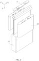
- FIG. 3 is a schematic exploded diagram of a structure of the battery cell 20 according to some embodiments of the present application.
- the battery cell 20 is the smallest unit of the battery. As shown in FIG. 3 , the battery cell 20 includes an end cap 21, a housing 22, a cell assembly 23 (hereinafter also referred to as a cell), and other functional components.
- the method 400 for detecting a defect on a surface of a cell may include the following steps S401 to S403.
- step S401 an initial image 500 of the surface of the cell is obtained by using an image acquisition unit (not shown).
- step S402 the initial image 500 is preprocessed to obtain at least one image 512 to be detected of the surface of the cell.
- step S403 the at least one image 512 to be detected is inputted into a defect detection neural network model, and a detection result outputted by the defect detection neural network model is obtained, the detection result being used to indicate whether there is a defect 511 on the surface of the cell.
- the obtained initial image 500 includes at least a cell surface area 510.
- the initial image 500 may further include a clamp area 530 for fixing the cell, and a background area 520 other than the cell surface area 510 and the clamp area 530.
- the defect 511 on the surface of the cell may be, for example, an indentation defect, a scratch defect, a bump defect, etc., and is not limited thereto in the present application.
- the at least one image 512 to be detected that is obtained after the preprocessing in step S402 may include one or more images to be detected.
- the defect on the surface of the cell accounts for a relatively large proportion
- only preprocessing operations such as exposure adjustment and color channel extraction may be performed on the initial image 500 without segmentation.
- the defect for example, an indentation defect
- the initial image 500 may be segmented to obtain a plurality of images p1...pn to be detected.
- the features of the defect in the image may include grayscale value, color, shape, contour, texture, etc.
- the defect detection neural network model may be a deep learning model, for example, ResNet18, a DNN, etc.
- a deep learning model may extract a plurality of features such as grayscale value, color, shape, contour, and texture from an image, so as to improve the accuracy of defect detection.
- the detection result outputted by the defect detection neural network model may include a corresponding defect confidence level of each image to be detected.
- the method 400 may be performed at a server or a client device.
- the server may include one or more general-purpose computers, a dedicated server computer (e.g., a personal computer (PC) server, a UNIX server, or a terminal server), a blade server, a mainframe computer, a server cluster, or any other suitable arrangement and/or combination.
- the server may be a server in a distributed system, a server combined with a blockchain, a cloud server, an intelligent cloud computing server or intelligent cloud host with artificial intelligence technologies, etc.
- the client device may include various types of computer devices, such as a portable handheld device, a general-purpose computer (such as a personal computer and a laptop computer), and a workstation computer.
- the method 400 may be performed at an industrial control computer equipped with a chip in the production line of cells.
- the chip may be a system on a chip (SoC) or the like.
- the initial image 500 is preprocessed, and the defect 511 in the preprocessed initial image 500 is detected by using the defect detection neural network model, so that features of the defect in the image may be made prominent, so as to facilitate subsequent detection of the defect detection neural network model; and more features may be extracted from the image, thereby improving the efficiency and accuracy of defect detection.
- the at least one image 512 to be detected includes a plurality of images p1...pn to be detected, and the initial image 500 contains a cell surface area 510 where the surface of the cell is located.
- the preprocessing the initial image 500 to obtain at least one image 512 to be detected of the surface of the cell in step S402 may include: extracting the cell surface area 510 from the initial image 500; and segmenting the cell surface area 510 to obtain the plurality of images 512 to be detected.
- the cell surface area 510 is first extracted from the initial image 500, and then the extracted cell surface area 510 is segmented to obtain the plurality of images p1...pn to be detected.
- the plurality of segmented images to be detected may have same sizes (as shown in FIG. 5 ), or may have different sizes, or some of the images may have same sizes and the other may have different sizes.
- the cell surface area is extracted and segmented to obtain the small-sized images to be detected, such that features of these defects are more prominent in the images to be detected, thereby improving the accuracy of defect detection.
- the initial image 500 has a first exposure.
- the extracting the cell surface area 510 from the initial image 500 may include: directly extracting the cell surface area 510 from the initial image 500; and adjusting an exposure of the cell surface area 510 to obtain a cell surface area 510a having a second exposure, where the first exposure is higher than the second exposure.
- the first exposure may be a high exposure.
- the image having the first exposure may be obtained in one or more manners of increasing an aperture size of an industrial camera, prolonging an exposure duration of the industrial camera, increasing the brightness in an environment, etc. Since there is generally a blue adhesive tape on the surface of the cell, the cell surface area 510 may be significantly distinguished from other areas (for example, a clamp area 530 and a background area 520) in the image having a higher exposure, that is, the initial image 500 (for example, the cell surface area and the other areas differ significantly in pixel value ranges).
- the cell surface area 510 having a high exposure some defects 511 (for example, an indentation defects) are difficult to be distinguished from other parts in the cell surface area 510 (for example, the cell surface area and the other areas differ slightly in pixel value ranges), as shown in FIG. 5 . Therefore, the cell surface area 510 having the first exposure is adjusted to the cell surface area 510a having the second exposure, so as to make the features of the defect 511 prominent in the cell surface area 510a, as shown in FIG. 5 .
- some defects 511 for example, an indentation defects
- the cell surface area 510 having the first exposure is adjusted to the cell surface area 510a having the second exposure, so as to make the features of the defect 511 prominent in the cell surface area 510a, as shown in FIG. 5 .
- the above implementation makes it easy to distinguish the cell surface area 510 from the other areas 520 and 530 in the initial image 500 having the first exposure, thereby facilitating the extraction of the cell surface area 510 from the initial image 500 having the first exposure.
- the color channel may be an R channel (red channel), G channel (green channel), or a B channel (blue channel). Because features of some defects 511 (for example, an indentation defect) are more prominent in an image with a specific color channel, the features of these defects may be made prominent in the extracted cell surface area with the preset color channel, as shown by the cell surface area 510b with the preset color channel in FIG. 5 .
- the preset color channel is a G channel.
- this facilitates subsequent detection of the defect detection neural network model on the defect in the cell surface area, so as to further improve the accuracy of defect detection.
- the directly extracting the cell surface area 510 from the initial image 500 may include: extracting the cell surface area 510 from the initial image 500 based at least on the pixel value range of the cell surface area.
- the initial image 500 may be an RGB image, and is not limited thereto in the present application.
- the pixel value may be a luminance value of each color channel of a color image.
- a pixel value of each pixel in an RGB image may include a luminance value, generally ranging from a minimum value of 0 to a maximum value of 255, of each color channel, that is, a red (R) channel, a green (G) channel, or a blue (B) channel.
- the pixel value range of the cell surface area 510 may be determined according to experience or requirements on battery production process specifications. For example, the pixel value range may be obtained based on a pixel value range for imaging of the surface of the cell under same illumination conditions.
- the above technical solution for extracting the cell surface area based on the pixel values of the areas in the initial image may quickly and effectively extract the cell surface area 510.
- the defect confidence level may be a probability value, which is used to evaluate a probability of the defect in the image to be detected.
- FIG. 6 shows detection results t1...tn outputted by a neural network model for corresponding images to be detected of a plurality of images to be detected, where an indentation defect 611 in an image to be detected corresponding to the detection result tn is the most prominent. It can be seen that the defect confidence level (that is, an indentation score) of the detection result tn outputted by the neural network model is the highest, that is, 0.996668, which indicates that the image to be detected corresponding to the detection result tn has the highest probability of having an indentation defect.
- a method 1000 for detecting a defect on a surface of a cell includes the following steps S1001 to S1011.
- step S1001 an initial image of the surface of the cell is obtained by using an image acquisition unit, the initial image having a first exposure.
- step S1002 a cell surface area is directly extracted from the initial image.
- step S1003 an exposure of the cell surface area is adjusted to obtain a cell surface area having a second exposure, where the first exposure is higher than the second exposure.
- step S1004 a cell surface area with a preset color channel is extracted from the cell surface area having the second exposure.
- step S1005 the cell surface area with the preset color channel is segmented to obtain a plurality of images to be detected.
- step S1006 the plurality of images to be detected are inputted into a defect detection neural network model, to obtain a defect confidence level of each of at least one image to be detected.
- step S1007 whether the defect confidence level of each of the plurality of images to be detected is less than or equal to a defect threshold is determined.
- step S1008 in response to determining that the defect confidence level of any one of the plurality of images to be detected is greater than the defect threshold, it is determined that there is a defect on the surface of the cell.
- step S1009 in response to determining that the defect confidence levels all of the plurality of images to be detected are less than or equal to the defect threshold, it is determined that there is no defect on the surface of the cell and an instruction that causes the cell to continue to be transferred to a next process is sent.
- Each step in the method 1000 has the same features as the corresponding step in the method 400. For the sake of brevity, this will not be repeated herein.
- features of the defect in the image may be made prominent, so as to facilitate subsequent detection of the defect detection neural network model; and more features may be extracted from the image, thereby helping recognizing the defect more efficiently, so as to improve the efficiency and accuracy of defect detection.
Landscapes
- Engineering & Computer Science (AREA)
- Physics & Mathematics (AREA)
- Theoretical Computer Science (AREA)
- General Physics & Mathematics (AREA)
- Computer Vision & Pattern Recognition (AREA)
- Quality & Reliability (AREA)
- General Health & Medical Sciences (AREA)
- Health & Medical Sciences (AREA)
- Artificial Intelligence (AREA)
- Evolutionary Computation (AREA)
- Software Systems (AREA)
- Life Sciences & Earth Sciences (AREA)
- Mathematical Physics (AREA)
- Biomedical Technology (AREA)
- Biophysics (AREA)
- Computational Linguistics (AREA)
- Data Mining & Analysis (AREA)
- General Engineering & Computer Science (AREA)
- Molecular Biology (AREA)
- Computing Systems (AREA)
- Radiology & Medical Imaging (AREA)
- Medical Informatics (AREA)
- Nuclear Medicine, Radiotherapy & Molecular Imaging (AREA)
- Image Analysis (AREA)
- Investigating Materials By The Use Of Optical Means Adapted For Particular Applications (AREA)
Claims (12)
- Procédé mis en œuvre par ordinateur (400) de détection d'un défaut sur une surface d'un élément de batterie, comprenant :l'obtention d'une image initiale (500) de la surface de l'élément en utilisant une unité d'acquisition d'images ;le prétraitement de l'image initiale (500) pour obtenir au moins une image (512) à détecter de la surface de l'élément ; etl'entrée de l'au moins une image (512) à détecter dans un modèle de réseau neuronal de détection de défauts, et l'obtention d'un résultat de détection délivré en sortie par le modèle de réseau neuronal de détection de défauts, le résultat de détection étant utilisé pour indiquer s'il existe ou non un défaut (511) sur la surface de l'élément, dans lequel l'au moins une image (512) à détecter comprend une pluralité d'images à détecter, et l'image initiale (500) contient une zone de surface d'élément (510) où la surface de l'élément est située ; etle prétraitement de l'image initiale (500) pour obtenir au moins une image à détecter de la surface de l'élément comprend :l'extraction de la zone de surface d'élément (510) de l'image initiale (500) ; etla segmentation de la zone de surface d'élément pour obtenir la pluralité d'images à détecter, dans lequel l'image initiale (500) présente une première exposition ; etl'extraction de la zone de surface d'élément (510) de l'image initiale (500) comprend :l'extraction directe de la zone de surface d'élément (510) de l'image initiale (500) ; etl'ajustement d'une exposition de la zone de surface d'élément (510) pour obtenir une zone de surface d'élément (510a) présentant une deuxième exposition, dans lequel la première exposition est supérieure à la deuxième exposition ; la première exposition est configurée de telle sorte qu'une plage de valeurs de pixels de la zone de surface d'élément (510) dans l'image initiale est différente d'une plage de valeurs de pixels de zones (520, 530) dans l'image initiale (500) autres que la zone de surface d'élément (510), et dans lequel l'extraction de la zone de surface d'élément (510) de l'image initiale comprend en outre :l'extraction d'une zone de surface d'élément (510b) avec un canal de couleur prédéfini de la zone de surface d'élément (510a) présentant la deuxième exposition ; etla segmentation de la zone de surface d'élément (510) pour obtenir la pluralité d'images à détecter comprend :
la segmentation de la zone de surface d'élément (510b) avec le canal de couleur prédéfini pour obtenir la pluralité d'images à détecter. - Procédé (400) selon la revendication 1, dans lequel le canal de couleur prédéfini est un canal G.
- Procédé (400) selon la revendication 1 ou la revendication 2, dans lequel l'extraction directe de la zone de surface d'élément (510) de l'image initiale (500) comprend :
l'extraction de la zone de surface d'élément (510) de l'image initiale (500) sur la base au moins de la plage de valeurs de pixels de la zone de surface d'élément. - Procédé (400) selon l'une quelconque des revendications 1 à 3, dans lequel la pluralité d'images à détecter présentent des tailles égales.
- Procédé (400) selon l'une quelconque des revendications 1 à 4, dans lequel le résultat de détection comprend un niveau de confiance de défaut correspondant de chacune des images à détecter, et l'entrée de l'au moins une image à détecter dans un modèle de réseau neuronal de détection de défauts, et l'obtention d'un résultat de détection délivré en sortie par le modèle de réseau neuronal de détection de défauts comprend :l'entrée de l'au moins une image à détecter dans le modèle de réseau neuronal de détection de défauts, pour obtenir un niveau de confiance de défaut de chacune de l'au moins une image (512) à détecter ; etla détermination, sur la base du niveau de confiance de défaut de chacune de l'au moins une image (512) à détecter, s'il existe ou non un défaut sur la surface de l'élément ; en option, la détermination, sur la base du niveau de confiance de défaut de chacune de l'au moins une image (512) à détecter, s'il existe ou non un défaut sur la surface de l'élément comprend :la détermination si le niveau de confiance de défaut de chacune de l'au moins une image (512) à détecter est inférieur ou égal à un seuil de défaut ; eten réponse à la détermination que les niveaux de confiance de défaut d'une ou plusieurs de l'au moins une image (512) à détecter sont supérieurs au seuil de défaut, la détermination qu'il existe un défaut sur la surface de l'élément.
- Procédé (400) selon l'une quelconque des revendications 1 à 5, dans lequel le défaut est un défaut d'indentation.
- Procédé (700) d'entraînement d'un modèle de réseau neuronal de détection de défauts, comprenant :l'obtention d'une image d'échantillon d'une surface d'un élément de batterie, l'image d'échantillon contenant un défaut prédéfini sur la surface de l'élément ;le prétraitement de l'image d'échantillon pour obtenir au moins une image d'échantillon à détecter de la surface de l'élément ;l'entrée de l'au moins une image d'échantillon à détecter dans le modèle de réseau neuronal de détection de défauts, et l'obtention d'un résultat de détection délivré en sortie par le modèle de réseau neuronal de détection de défauts, le résultat de détection étant utilisé pour indiquer s'il existe ou non un défaut sur la surface de l'élément ; etl'ajustement d'un paramètre du modèle de réseau neuronal de détection de défauts sur la base du résultat de détection et du défaut prédéfini, dans lequel l'au moins une image d'échantillon à détecter comprend une pluralité d'images d'échantillon à détecter et l'image d'échantillon contient une zone de surface d'élément où la surface de l'élément est située ; etle prétraitement de l'image d'échantillon pour obtenir au moins une image d'échantillon à détecter de la surface de l'élément comprend :et l'extraction de la zone de surface d'élément de l'image d'échantillon comprend en outre :l'extraction de la zone de surface d'élément de l'image d'échantillon ; etla segmentation de la zone de surface d'élément pour obtenir la pluralité d'images d'échantillon à détecter ;l'image d'échantillon présente une première exposition ; etl'extraction de la zone de surface d'élément de l'image d'échantillon comprend :l'extraction directe de la zone de surface d'élément de l'image d'échantillon ; etl'ajustement d'une exposition de la zone de surface d'élément pour obtenir une zone de surface d'élément présentant une deuxième exposition,dans lequel la première exposition est supérieure à la deuxième exposition ;l'extraction d'une zone de surface d'élément avec un canal de couleur prédéfini de la zone de surface d'élément présentant la deuxième exposition ; etla segmentation de la zone de surface d'élément pour obtenir la pluralité d'images d'échantillon à détecter comprend :
la segmentation de la zone de surface d'élément avec le canal de couleur prédéfini pour obtenir la pluralité d'images d'échantillon à détecter. - Appareil (800) de détection d'un défaut d'indentation sur une surface d'un élément, comprenant des moyens pour effectuer le procédé selon l'une quelconque des revendications 1 - 6 comprenant :une unité d'obtention (801) configurée pour obtenir une image initiale de la surface de l'élément en utilisant une unité d'acquisition d'images ;une unité de prétraitement (802) configurée pour prétraiter l'image initiale pour obtenir au moins une image à détecter de la surface de l'élément ; etune unité de détection (803) configurée pour entrer l'au moins une image à détecter dans un modèle de réseau neuronal de détection de défauts, et pour obtenir un résultat de détection délivré en sortie par le modèle de réseau neuronal de détection de défauts, le résultat de détection étant utilisé pour indiquer s'il existe ou non un défaut sur la surface de l'élément.
- Appareil (900) pour entraîner un modèle de réseau neuronal de détection de défauts, comprenant des moyens pour effectuer le procédé selon la revendication 7, comprenant :une unité d'obtention d'image (901) configurée pour obtenir une image d'échantillon d'une surface d'un élément, l'image d'échantillon contenant un défaut prédéfini sur la surface de l'élément ;une unité de traitement d'image (902), configurée pour prétraiter l'image d'échantillon pour obtenir au moins une image d'échantillon à détecter de la surface de l'élément ;une unité de détection de défauts (903) configurée pour entrer l'au moins une image d'échantillon à détecter dans le modèle de réseau neuronal de détection de défauts, et pour obtenir un résultat de détection délivré en sortie par le modèle de réseau neuronal de détection de défauts, le résultat de détection étant utilisé pour indiquer s'il existe ou non un défaut sur la surface de l'élément ; etune unité d'ajustement (904) configurée pour ajuster un paramètre du modèle de réseau neuronal de détection de défauts sur la base du résultat de détection et du défaut prédéfini.
- Dispositif électronique, comprenant au moins un processeur et une mémoire connectée en communication à l'au moins un processeur, dans lequel
la mémoire stocke des instructions pouvant être exécutées par l'au moins un processeur, et les instructions, lorsqu'elles sont exécutées par l'au moins un processeur, amènent l'au moins un processeur à réaliser un procédé selon l'une quelconque des revendications 1 à 6 et/ou un procédé selon la revendication 7. - Support de stockage lisible par ordinateur stockant des instructions informatiques, dans lequel les instructions informatiques sont utilisées pour amener un ordinateur à réaliser un procédé selon l'une quelconque des revendications 1 à 6 et/ou un procédé selon la revendication 7.
- Produit de programme informatique, comprenant un programme informatique, dans lequel le programme informatique, lorsqu'il est exécuté par un processeur, met en œuvre un procédé selon l'une quelconque des revendications 1 à 6 et/ou un procédé selon la revendication 7.
Applications Claiming Priority (2)
| Application Number | Priority Date | Filing Date | Title |
|---|---|---|---|
| CN202210907837.9A CN115829912A (zh) | 2022-07-29 | 2022-07-29 | 检测电芯表面缺陷的方法和装置 |
| PCT/CN2023/085076 WO2024021662A1 (fr) | 2022-07-29 | 2023-03-30 | Procédé et appareil de détection de défaut de surface de cellule de batterie |
Publications (4)
| Publication Number | Publication Date |
|---|---|
| EP4336443A1 EP4336443A1 (fr) | 2024-03-13 |
| EP4336443A4 EP4336443A4 (fr) | 2024-08-07 |
| EP4336443B1 true EP4336443B1 (fr) | 2025-04-16 |
| EP4336443C0 EP4336443C0 (fr) | 2025-04-16 |
Family
ID=85522990
Family Applications (1)
| Application Number | Title | Priority Date | Filing Date |
|---|---|---|---|
| EP23744030.0A Active EP4336443B1 (fr) | 2022-07-29 | 2023-03-30 | Procédé et appareil de détection de défaut de surface de cellule de batterie |
Country Status (6)
| Country | Link |
|---|---|
| US (1) | US12406349B2 (fr) |
| EP (1) | EP4336443B1 (fr) |
| CN (1) | CN115829912A (fr) |
| ES (1) | ES3035473T3 (fr) |
| HU (1) | HUE071907T2 (fr) |
| WO (1) | WO2024021662A1 (fr) |
Families Citing this family (17)
| Publication number | Priority date | Publication date | Assignee | Title |
|---|---|---|---|---|
| CN115829912A (zh) * | 2022-07-29 | 2023-03-21 | 宁德时代新能源科技股份有限公司 | 检测电芯表面缺陷的方法和装置 |
| CN116067619B (zh) * | 2023-03-07 | 2023-08-11 | 宁德时代新能源科技股份有限公司 | 电池卷绕检测装置、卷绕装置、检测方法、设备和介质 |
| CN116630262B (zh) * | 2023-05-17 | 2025-02-07 | 江苏正力新能电池技术股份有限公司 | 基于神经网络的电芯检测方法和系统 |
| CN116309564B (zh) * | 2023-05-17 | 2023-08-11 | 厦门微图软件科技有限公司 | 基于人工智能图像识别的电芯外观缺陷检测方法及系统 |
| CN116543267B (zh) * | 2023-07-04 | 2023-10-13 | 宁德时代新能源科技股份有限公司 | 图像集处理方法、图像分割方法、装置、设备和存储介质 |
| KR20250097416A (ko) * | 2023-12-21 | 2025-06-30 | 삼성에스디아이 주식회사 | 배터리 진단 장치 및 방법, 컴퓨터 프로그램 |
| CN117611591B (zh) * | 2024-01-24 | 2024-05-14 | 俐玛精密测量技术(苏州)有限公司 | 电芯缺陷的工业ct检测方法、装置、电子设备及存储介质 |
| CN117723491B (zh) * | 2024-02-07 | 2024-07-23 | 宁德时代新能源科技股份有限公司 | 电芯防爆阀的检测系统及检测方法 |
| CN120612269B (zh) * | 2024-03-07 | 2026-07-03 | 上海集成电路装备材料产业创新中心有限公司 | 一种芯片异常的检测方法、装置、设备及存储介质 |
| CN117929280B (zh) * | 2024-03-21 | 2024-09-06 | 宁德时代新能源科技股份有限公司 | 电池蓝膜包覆系统及电池蓝膜包覆的检测方法 |
| CN118037740A (zh) * | 2024-04-15 | 2024-05-14 | 宁德时代新能源科技股份有限公司 | 极片检测方法、装置、设备、存储介质和计算机程序产品 |
| CN118311043B (zh) * | 2024-06-13 | 2024-10-18 | 宁德时代新能源科技股份有限公司 | 电芯绝缘膜检测系统及其方法 |
| CN118570554A (zh) * | 2024-07-17 | 2024-08-30 | 敬业钢铁有限公司 | 基于图像处理的钢铁缺陷预测方法及系统 |
| CN119780093A (zh) * | 2024-11-05 | 2025-04-08 | 比亚迪股份有限公司 | 金属异物检测系统、方法、装置、设备及存储介质 |
| CN119515840A (zh) * | 2024-11-13 | 2025-02-25 | 曲靖亿纬锂能有限公司 | 电芯外观检测方法和装置、存储介质及电子设备 |
| CN120122578A (zh) * | 2025-02-24 | 2025-06-10 | 青岛贝斯兰半导体科技有限公司 | 一种隔膜泵的生产过程控制方法、设备及介质 |
| CN121661017B (zh) * | 2025-12-08 | 2026-06-26 | 杭州安脉盛智能技术有限公司 | 一种工业零部件缺陷检测方法、装置、设备及存储介质 |
Family Cites Families (15)
| Publication number | Priority date | Publication date | Assignee | Title |
|---|---|---|---|---|
| KR101030449B1 (ko) * | 2009-08-17 | 2011-04-25 | 홍익대학교 산학협력단 | 원통형 이차 전지 외관 검사 장치 |
| CN109472284A (zh) * | 2018-09-18 | 2019-03-15 | 浙江大学 | 一种基于无偏嵌入零样本学习的电芯缺陷分类方法 |
| CN109598721B (zh) * | 2018-12-10 | 2021-08-31 | 广州市易鸿智能装备有限公司 | 电池极片的缺陷检测方法、装置、检测设备和存储介质 |
| CN111060514B (zh) * | 2019-12-02 | 2022-11-04 | 精锐视觉智能科技(上海)有限公司 | 缺陷检测方法、装置及终端设备 |
| CN111179253B (zh) * | 2019-12-30 | 2023-11-24 | 歌尔股份有限公司 | 一种产品缺陷检测方法、装置与系统 |
| CN111640091B (zh) * | 2020-05-14 | 2023-08-22 | 阿丘机器人科技(苏州)有限公司 | 产品缺陷的检测方法及计算机存储介质 |
| CN111598877B (zh) * | 2020-05-18 | 2022-08-09 | 河北工业大学 | 一种基于生成对抗网络的锂电池表面缺陷检测方法 |
| CN111693534B (zh) * | 2020-06-12 | 2023-09-15 | 北京百度网讯科技有限公司 | 表面缺陷的检测方法、模型训练方法、装置、设备和介质 |
| CN112241699B (zh) * | 2020-10-13 | 2024-07-05 | 无锡先导智能装备股份有限公司 | 物体缺陷类别识别方法、装置、计算机设备和存储介质 |
| CN112634254A (zh) * | 2020-12-29 | 2021-04-09 | 北京市商汤科技开发有限公司 | 绝缘子缺陷检测方法及相关装置 |
| CN113222950B (zh) * | 2021-05-19 | 2023-07-07 | 广东奥普特科技股份有限公司 | 表面缺陷检测模型训练方法、表面缺陷检测方法及系统 |
| CN113092489B (zh) * | 2021-05-20 | 2024-08-23 | 鲸朵(上海)智能科技有限公司 | 一种电池外观缺陷的检测系统及方法 |
| CN114782310A (zh) * | 2022-03-08 | 2022-07-22 | 江苏立导科技有限公司 | 表面缺陷检测方法、装置、设备和存储介质 |
| CN117813624A (zh) * | 2022-07-29 | 2024-04-02 | 宁德时代新能源科技股份有限公司 | 用于电芯的缺陷检测模型的训练方法和训练装置 |
| CN115829912A (zh) * | 2022-07-29 | 2023-03-21 | 宁德时代新能源科技股份有限公司 | 检测电芯表面缺陷的方法和装置 |
-
2022
- 2022-07-29 CN CN202210907837.9A patent/CN115829912A/zh active Pending
-
2023
- 2023-03-30 HU HUE23744030A patent/HUE071907T2/hu unknown
- 2023-03-30 EP EP23744030.0A patent/EP4336443B1/fr active Active
- 2023-03-30 WO PCT/CN2023/085076 patent/WO2024021662A1/fr not_active Ceased
- 2023-03-30 ES ES23744030T patent/ES3035473T3/es active Active
- 2023-08-23 US US18/454,184 patent/US12406349B2/en active Active
Also Published As
| Publication number | Publication date |
|---|---|
| ES3035473T3 (en) | 2025-09-03 |
| HUE071907T2 (hu) | 2025-10-28 |
| WO2024021662A1 (fr) | 2024-02-01 |
| US12406349B2 (en) | 2025-09-02 |
| US20240037726A1 (en) | 2024-02-01 |
| CN115829912A (zh) | 2023-03-21 |
| EP4336443A1 (fr) | 2024-03-13 |
| EP4336443C0 (fr) | 2025-04-16 |
| EP4336443A4 (fr) | 2024-08-07 |
Similar Documents
| Publication | Publication Date | Title |
|---|---|---|
| EP4336443A1 (fr) | Procédé et appareil de détection de défaut de surface de cellule de batterie | |
| EP4350334B1 (fr) | Procédé, appareil et système de détection d'élément de batterie, et dispositif informatique et support de stockage | |
| EP4407302A1 (fr) | Appareil de détection optique, procédé et appareil de détection, dispositif électronique et support de stockage | |
| EP4383398A1 (fr) | Procédé et appareil de détection de défaut de revêtement isolant d'une plaque d'électrode de batterie, et dispositif informatique | |
| US11763549B1 (en) | Method and apparatus for training cell defect detection model | |
| US20230140944A1 (en) | Battery Cell Exterior Inspection System | |
| US20240221150A1 (en) | Electrode plate wrinkling detection method and system, terminal, and storage medium | |
| CN116523921B (zh) | 一种针对极耳翻折情况的检测方法、装置和系统 | |
| US11915410B2 (en) | Method and apparatus for inspecting tab appearance of cell assembly, and electronic device | |
| CN115829908A (zh) | 对复合料带的阴极极片进行折角检测的方法、装置和系统 | |
| US12631575B2 (en) | Battery defect inspection device, method, and apparatus | |
| US20240210481A1 (en) | Method and apparatus for identifying abnormal battery cell, electronic device, and storage medium | |
| EP4354396B1 (fr) | Procédé et dispositif de correction d'image de profondeur, et procédé de détection de soudage pour un ensemble boîtier de batterie | |
| CN114565551A (zh) | 标签检测方法、装置、设备和计算机可读存储介质 | |
| CN115861214A (zh) | 转接片的检测方法、装置、电池单体的生产方法和设备 | |
| CN118229675B (zh) | 电芯检测方法及系统 | |
| CN118789124B (zh) | 基于动力锂电池退役回收梯次利用热切割处理设备及方法 | |
| CN120142285A (zh) | 电池离子析出检测方法及检测装置 | |
| KR20250052876A (ko) | 배터리 이미지 분석 장치 및 그의 동작 방법 | |
| KR20250085465A (ko) | 배터리 진단 장치 및 배터리 진단 방법 | |
| CN119251128A (zh) | 图像检测模型及其训练方法、电池检测方法和设备 |
Legal Events
| Date | Code | Title | Description |
|---|---|---|---|
| STAA | Information on the status of an ep patent application or granted ep patent |
Free format text: STATUS: UNKNOWN |
|
| STAA | Information on the status of an ep patent application or granted ep patent |
Free format text: STATUS: THE INTERNATIONAL PUBLICATION HAS BEEN MADE |
|
| PUAI | Public reference made under article 153(3) epc to a published international application that has entered the european phase |
Free format text: ORIGINAL CODE: 0009012 |
|
| STAA | Information on the status of an ep patent application or granted ep patent |
Free format text: STATUS: REQUEST FOR EXAMINATION WAS MADE |
|
| 17P | Request for examination filed |
Effective date: 20230731 |
|
| AK | Designated contracting states |
Kind code of ref document: A1 Designated state(s): AL AT BE BG CH CY CZ DE DK EE ES FI FR GB GR HR HU IE IS IT LI LT LU LV MC ME MK MT NL NO PL PT RO RS SE SI SK SM TR |
|
| A4 | Supplementary search report drawn up and despatched |
Effective date: 20240705 |
|
| RIC1 | Information provided on ipc code assigned before grant |
Ipc: G06N 3/08 20230101ALI20240701BHEP Ipc: G06N 3/04 20230101ALI20240701BHEP Ipc: G06T 7/90 20170101ALI20240701BHEP Ipc: G06T 7/11 20170101ALI20240701BHEP Ipc: G06T 7/00 20170101AFI20240701BHEP |
|
| RAP1 | Party data changed (applicant data changed or rights of an application transferred) |
Owner name: CONTEMPORARY AMPEREX TECHNOLOGY(HONG KONG) LIMITED |
|
| GRAP | Despatch of communication of intention to grant a patent |
Free format text: ORIGINAL CODE: EPIDOSNIGR1 |
|
| STAA | Information on the status of an ep patent application or granted ep patent |
Free format text: STATUS: GRANT OF PATENT IS INTENDED |
|
| GRAS | Grant fee paid |
Free format text: ORIGINAL CODE: EPIDOSNIGR3 |
|
| GRAA | (expected) grant |
Free format text: ORIGINAL CODE: 0009210 |
|
| STAA | Information on the status of an ep patent application or granted ep patent |
Free format text: STATUS: THE PATENT HAS BEEN GRANTED |
|
| DAV | Request for validation of the european patent (deleted) | ||
| DAX | Request for extension of the european patent (deleted) | ||
| INTG | Intention to grant announced |
Effective date: 20250218 |
|
| AK | Designated contracting states |
Kind code of ref document: B1 Designated state(s): AL AT BE BG CH CY CZ DE DK EE ES FI FR GB GR HR HU IE IS IT LI LT LU LV MC ME MK MT NL NO PL PT RO RS SE SI SK SM TR |
|
| REG | Reference to a national code |
Ref country code: GB Ref legal event code: FG4D |
|
| REG | Reference to a national code |
Ref country code: CH Ref legal event code: EP |
|
| REG | Reference to a national code |
Ref country code: IE Ref legal event code: FG4D |
|
| REG | Reference to a national code |
Ref country code: DE Ref legal event code: R096 Ref document number: 602023002983 Country of ref document: DE |
|
| U01 | Request for unitary effect filed |
Effective date: 20250509 |
|
| U07 | Unitary effect registered |
Designated state(s): AT BE BG DE DK EE FI FR IT LT LU LV MT NL PT RO SE SI Effective date: 20250516 |
|
| REG | Reference to a national code |
Ref country code: ES Ref legal event code: FG2A Ref document number: 3035473 Country of ref document: ES Kind code of ref document: T3 Effective date: 20250903 |
|
| PG25 | Lapsed in a contracting state [announced via postgrant information from national office to epo] |
Ref country code: GR Free format text: LAPSE BECAUSE OF FAILURE TO SUBMIT A TRANSLATION OF THE DESCRIPTION OR TO PAY THE FEE WITHIN THE PRESCRIBED TIME-LIMIT Effective date: 20250717 Ref country code: NO Free format text: LAPSE BECAUSE OF FAILURE TO SUBMIT A TRANSLATION OF THE DESCRIPTION OR TO PAY THE FEE WITHIN THE PRESCRIBED TIME-LIMIT Effective date: 20250716 |
|
| PG25 | Lapsed in a contracting state [announced via postgrant information from national office to epo] |
Ref country code: PL Free format text: LAPSE BECAUSE OF FAILURE TO SUBMIT A TRANSLATION OF THE DESCRIPTION OR TO PAY THE FEE WITHIN THE PRESCRIBED TIME-LIMIT Effective date: 20250416 |
|
| PG25 | Lapsed in a contracting state [announced via postgrant information from national office to epo] |
Ref country code: HR Free format text: LAPSE BECAUSE OF FAILURE TO SUBMIT A TRANSLATION OF THE DESCRIPTION OR TO PAY THE FEE WITHIN THE PRESCRIBED TIME-LIMIT Effective date: 20250416 |
|
| PG25 | Lapsed in a contracting state [announced via postgrant information from national office to epo] |
Ref country code: RS Free format text: LAPSE BECAUSE OF FAILURE TO SUBMIT A TRANSLATION OF THE DESCRIPTION OR TO PAY THE FEE WITHIN THE PRESCRIBED TIME-LIMIT Effective date: 20250716 |
|
| PG25 | Lapsed in a contracting state [announced via postgrant information from national office to epo] |
Ref country code: IS Free format text: LAPSE BECAUSE OF FAILURE TO SUBMIT A TRANSLATION OF THE DESCRIPTION OR TO PAY THE FEE WITHIN THE PRESCRIBED TIME-LIMIT Effective date: 20250816 |
|
| REG | Reference to a national code |
Ref country code: HU Ref legal event code: AG4A Ref document number: E071907 Country of ref document: HU |
|
| PG25 | Lapsed in a contracting state [announced via postgrant information from national office to epo] |
Ref country code: SM Free format text: LAPSE BECAUSE OF FAILURE TO SUBMIT A TRANSLATION OF THE DESCRIPTION OR TO PAY THE FEE WITHIN THE PRESCRIBED TIME-LIMIT Effective date: 20250416 |
|
| PG25 | Lapsed in a contracting state [announced via postgrant information from national office to epo] |
Ref country code: CZ Free format text: LAPSE BECAUSE OF FAILURE TO SUBMIT A TRANSLATION OF THE DESCRIPTION OR TO PAY THE FEE WITHIN THE PRESCRIBED TIME-LIMIT Effective date: 20250416 |
|
| PG25 | Lapsed in a contracting state [announced via postgrant information from national office to epo] |
Ref country code: SK Free format text: LAPSE BECAUSE OF FAILURE TO SUBMIT A TRANSLATION OF THE DESCRIPTION OR TO PAY THE FEE WITHIN THE PRESCRIBED TIME-LIMIT Effective date: 20250416 |
|
| PLBE | No opposition filed within time limit |
Free format text: ORIGINAL CODE: 0009261 |
|
| STAA | Information on the status of an ep patent application or granted ep patent |
Free format text: STATUS: NO OPPOSITION FILED WITHIN TIME LIMIT |
|
| REG | Reference to a national code |
Ref country code: CH Ref legal event code: L10 Free format text: ST27 STATUS EVENT CODE: U-0-0-L10-L00 (AS PROVIDED BY THE NATIONAL OFFICE) Effective date: 20260225 |
|
| 26N | No opposition filed |
Effective date: 20260119 |
|
| PGFP | Annual fee paid to national office [announced via postgrant information from national office to epo] |
Ref country code: HU Payment date: 20260316 Year of fee payment: 4 |
|
| U20 | Renewal fee for the european patent with unitary effect paid |
Year of fee payment: 4 Effective date: 20260325 |
|
| PGFP | Annual fee paid to national office [announced via postgrant information from national office to epo] |
Ref country code: ES Payment date: 20260401 Year of fee payment: 4 |