EP4336544A2 - Halbleiterstruktur mit verbesserter spannungsfestigkeit - Google Patents
Halbleiterstruktur mit verbesserter spannungsfestigkeit Download PDFInfo
- Publication number
- EP4336544A2 EP4336544A2 EP23219424.1A EP23219424A EP4336544A2 EP 4336544 A2 EP4336544 A2 EP 4336544A2 EP 23219424 A EP23219424 A EP 23219424A EP 4336544 A2 EP4336544 A2 EP 4336544A2
- Authority
- EP
- European Patent Office
- Prior art keywords
- layer
- semiconductor structure
- superlattice
- interlayer
- thickness
- Prior art date
- Legal status (The legal status is an assumption and is not a legal conclusion. Google has not performed a legal analysis and makes no representation as to the accuracy of the status listed.)
- Pending
Links
Images
Classifications
-
- H—ELECTRICITY
- H10—SEMICONDUCTOR DEVICES; ELECTRIC SOLID-STATE DEVICES NOT OTHERWISE PROVIDED FOR
- H10D—INORGANIC ELECTRIC SEMICONDUCTOR DEVICES
- H10D62/00—Semiconductor bodies, or regions thereof, of devices having potential barriers
- H10D62/80—Semiconductor bodies, or regions thereof, of devices having potential barriers characterised by the materials
- H10D62/81—Semiconductor bodies, or regions thereof, of devices having potential barriers characterised by the materials of structures exhibiting quantum-confinement effects, e.g. single quantum wells; of structures having periodic or quasi-periodic potential variation
- H10D62/815—Semiconductor bodies, or regions thereof, of devices having potential barriers characterised by the materials of structures exhibiting quantum-confinement effects, e.g. single quantum wells; of structures having periodic or quasi-periodic potential variation of structures having periodic or quasi-periodic potential variation, e.g. superlattices or multiple quantum wells [MQW]
- H10D62/8161—Semiconductor bodies, or regions thereof, of devices having potential barriers characterised by the materials of structures exhibiting quantum-confinement effects, e.g. single quantum wells; of structures having periodic or quasi-periodic potential variation of structures having periodic or quasi-periodic potential variation, e.g. superlattices or multiple quantum wells [MQW] potential variation due to variations in composition or crystallinity, e.g. heterojunction superlattices
- H10D62/8162—Semiconductor bodies, or regions thereof, of devices having potential barriers characterised by the materials of structures exhibiting quantum-confinement effects, e.g. single quantum wells; of structures having periodic or quasi-periodic potential variation of structures having periodic or quasi-periodic potential variation, e.g. superlattices or multiple quantum wells [MQW] potential variation due to variations in composition or crystallinity, e.g. heterojunction superlattices having quantum effects only in the vertical direction, i.e. layered structures having quantum effects solely resulting from vertical potential variation
- H10D62/8164—Semiconductor bodies, or regions thereof, of devices having potential barriers characterised by the materials of structures exhibiting quantum-confinement effects, e.g. single quantum wells; of structures having periodic or quasi-periodic potential variation of structures having periodic or quasi-periodic potential variation, e.g. superlattices or multiple quantum wells [MQW] potential variation due to variations in composition or crystallinity, e.g. heterojunction superlattices having quantum effects only in the vertical direction, i.e. layered structures having quantum effects solely resulting from vertical potential variation comprising only semiconductor materials
-
- H—ELECTRICITY
- H10—SEMICONDUCTOR DEVICES; ELECTRIC SOLID-STATE DEVICES NOT OTHERWISE PROVIDED FOR
- H10D—INORGANIC ELECTRIC SEMICONDUCTOR DEVICES
- H10D30/00—Field-effect transistors [FET]
- H10D30/40—FETs having zero-dimensional [0D], one-dimensional [1D] or two-dimensional [2D] charge carrier gas channels
- H10D30/47—FETs having zero-dimensional [0D], one-dimensional [1D] or two-dimensional [2D] charge carrier gas channels having two-dimensional [2D] charge carrier gas channels, e.g. nanoribbon FETs or high electron mobility transistors [HEMT]
- H10D30/471—High electron mobility transistors [HEMT] or high hole mobility transistors [HHMT]
- H10D30/475—High electron mobility transistors [HEMT] or high hole mobility transistors [HHMT] having wider bandgap layer formed on top of lower bandgap active layer, e.g. undoped barrier HEMTs such as i-AlGaN/GaN HEMTs
-
- H—ELECTRICITY
- H10—SEMICONDUCTOR DEVICES; ELECTRIC SOLID-STATE DEVICES NOT OTHERWISE PROVIDED FOR
- H10P—GENERIC PROCESSES OR APPARATUS FOR THE MANUFACTURE OR TREATMENT OF DEVICES COVERED BY CLASS H10
- H10P14/00—Formation of materials, e.g. in the shape of layers or pillars
- H10P14/20—Formation of materials, e.g. in the shape of layers or pillars of semiconductor materials
- H10P14/24—Formation of materials, e.g. in the shape of layers or pillars of semiconductor materials using chemical vapour deposition [CVD]
-
- H—ELECTRICITY
- H10—SEMICONDUCTOR DEVICES; ELECTRIC SOLID-STATE DEVICES NOT OTHERWISE PROVIDED FOR
- H10P—GENERIC PROCESSES OR APPARATUS FOR THE MANUFACTURE OR TREATMENT OF DEVICES COVERED BY CLASS H10
- H10P14/00—Formation of materials, e.g. in the shape of layers or pillars
- H10P14/20—Formation of materials, e.g. in the shape of layers or pillars of semiconductor materials
- H10P14/29—Formation of materials, e.g. in the shape of layers or pillars of semiconductor materials characterised by the substrates
- H10P14/2901—Materials
- H10P14/2902—Materials being Group IVA materials
- H10P14/2905—Silicon, silicon germanium or germanium
-
- H—ELECTRICITY
- H10—SEMICONDUCTOR DEVICES; ELECTRIC SOLID-STATE DEVICES NOT OTHERWISE PROVIDED FOR
- H10P—GENERIC PROCESSES OR APPARATUS FOR THE MANUFACTURE OR TREATMENT OF DEVICES COVERED BY CLASS H10
- H10P14/00—Formation of materials, e.g. in the shape of layers or pillars
- H10P14/20—Formation of materials, e.g. in the shape of layers or pillars of semiconductor materials
- H10P14/29—Formation of materials, e.g. in the shape of layers or pillars of semiconductor materials characterised by the substrates
- H10P14/2924—Structures
-
- H—ELECTRICITY
- H10—SEMICONDUCTOR DEVICES; ELECTRIC SOLID-STATE DEVICES NOT OTHERWISE PROVIDED FOR
- H10P—GENERIC PROCESSES OR APPARATUS FOR THE MANUFACTURE OR TREATMENT OF DEVICES COVERED BY CLASS H10
- H10P14/00—Formation of materials, e.g. in the shape of layers or pillars
- H10P14/20—Formation of materials, e.g. in the shape of layers or pillars of semiconductor materials
- H10P14/29—Formation of materials, e.g. in the shape of layers or pillars of semiconductor materials characterised by the substrates
- H10P14/2926—Crystal orientations
-
- H—ELECTRICITY
- H10—SEMICONDUCTOR DEVICES; ELECTRIC SOLID-STATE DEVICES NOT OTHERWISE PROVIDED FOR
- H10P—GENERIC PROCESSES OR APPARATUS FOR THE MANUFACTURE OR TREATMENT OF DEVICES COVERED BY CLASS H10
- H10P14/00—Formation of materials, e.g. in the shape of layers or pillars
- H10P14/20—Formation of materials, e.g. in the shape of layers or pillars of semiconductor materials
- H10P14/32—Formation of materials, e.g. in the shape of layers or pillars of semiconductor materials characterised by intermediate layers between substrates and deposited layers
- H10P14/3202—Materials thereof
- H10P14/3214—Materials thereof being Group IIIA-VA semiconductors
- H10P14/3216—Nitrides
-
- H—ELECTRICITY
- H10—SEMICONDUCTOR DEVICES; ELECTRIC SOLID-STATE DEVICES NOT OTHERWISE PROVIDED FOR
- H10P—GENERIC PROCESSES OR APPARATUS FOR THE MANUFACTURE OR TREATMENT OF DEVICES COVERED BY CLASS H10
- H10P14/00—Formation of materials, e.g. in the shape of layers or pillars
- H10P14/20—Formation of materials, e.g. in the shape of layers or pillars of semiconductor materials
- H10P14/32—Formation of materials, e.g. in the shape of layers or pillars of semiconductor materials characterised by intermediate layers between substrates and deposited layers
- H10P14/3242—Structure
- H10P14/3244—Layer structure
- H10P14/3251—Layer structure consisting of three or more layers
- H10P14/3252—Alternating layers, e.g. superlattice
-
- H—ELECTRICITY
- H10—SEMICONDUCTOR DEVICES; ELECTRIC SOLID-STATE DEVICES NOT OTHERWISE PROVIDED FOR
- H10P—GENERIC PROCESSES OR APPARATUS FOR THE MANUFACTURE OR TREATMENT OF DEVICES COVERED BY CLASS H10
- H10P14/00—Formation of materials, e.g. in the shape of layers or pillars
- H10P14/20—Formation of materials, e.g. in the shape of layers or pillars of semiconductor materials
- H10P14/34—Deposited materials, e.g. layers
- H10P14/3402—Deposited materials, e.g. layers characterised by the chemical composition
- H10P14/3414—Deposited materials, e.g. layers characterised by the chemical composition being group IIIA-VIA materials
- H10P14/3416—Nitrides
-
- H—ELECTRICITY
- H10—SEMICONDUCTOR DEVICES; ELECTRIC SOLID-STATE DEVICES NOT OTHERWISE PROVIDED FOR
- H10P—GENERIC PROCESSES OR APPARATUS FOR THE MANUFACTURE OR TREATMENT OF DEVICES COVERED BY CLASS H10
- H10P14/00—Formation of materials, e.g. in the shape of layers or pillars
- H10P14/20—Formation of materials, e.g. in the shape of layers or pillars of semiconductor materials
- H10P14/34—Deposited materials, e.g. layers
- H10P14/3438—Doping during depositing
- H10P14/3441—Conductivity type
- H10P14/3444—P-type
-
- H—ELECTRICITY
- H10—SEMICONDUCTOR DEVICES; ELECTRIC SOLID-STATE DEVICES NOT OTHERWISE PROVIDED FOR
- H10D—INORGANIC ELECTRIC SEMICONDUCTOR DEVICES
- H10D30/00—Field-effect transistors [FET]
- H10D30/40—FETs having zero-dimensional [0D], one-dimensional [1D] or two-dimensional [2D] charge carrier gas channels
- H10D30/47—FETs having zero-dimensional [0D], one-dimensional [1D] or two-dimensional [2D] charge carrier gas channels having two-dimensional [2D] charge carrier gas channels, e.g. nanoribbon FETs or high electron mobility transistors [HEMT]
-
- H—ELECTRICITY
- H10—SEMICONDUCTOR DEVICES; ELECTRIC SOLID-STATE DEVICES NOT OTHERWISE PROVIDED FOR
- H10D—INORGANIC ELECTRIC SEMICONDUCTOR DEVICES
- H10D62/00—Semiconductor bodies, or regions thereof, of devices having potential barriers
- H10D62/80—Semiconductor bodies, or regions thereof, of devices having potential barriers characterised by the materials
- H10D62/85—Semiconductor bodies, or regions thereof, of devices having potential barriers characterised by the materials being Group III-V materials, e.g. GaAs
- H10D62/8503—Nitride Group III-V materials, e.g. AlN or GaN
-
- H—ELECTRICITY
- H10—SEMICONDUCTOR DEVICES; ELECTRIC SOLID-STATE DEVICES NOT OTHERWISE PROVIDED FOR
- H10D—INORGANIC ELECTRIC SEMICONDUCTOR DEVICES
- H10D62/00—Semiconductor bodies, or regions thereof, of devices having potential barriers
- H10D62/80—Semiconductor bodies, or regions thereof, of devices having potential barriers characterised by the materials
- H10D62/85—Semiconductor bodies, or regions thereof, of devices having potential barriers characterised by the materials being Group III-V materials, e.g. GaAs
- H10D62/854—Semiconductor bodies, or regions thereof, of devices having potential barriers characterised by the materials being Group III-V materials, e.g. GaAs further characterised by the dopants
Definitions
- the present invention relates to a semiconductor structure having improved voltage withstand.
- GaN or Gallium nitride makes it possible to produce good quality electronic devices.
- GaN and silicon do not have the same mesh parameters nor close or equal thermal expansion coefficients. Thus, if no precautions are taken, the GaN obtained is not of good quality and, during cooling after the deposition of the GaN, cracks appear in the layer(s) of GaN.
- one or more buffer layers are interposed between the substrate and the layer(s) of GaN, these imposing compressive stresses in the GaN, which during cooling prevents the appearance of cracks in the layer. of GaN.
- the presence of the buffer layer(s) prevents the GaN from being in contact with the silicon, which would otherwise cause the appearance of crystal defects in the GaN.
- the material of the buffer layer is for example AlN.
- the document WO2013001014 describes a semiconductor structure comprising a thick GaN layer.
- This thick GaN layer is obtained by producing, on an AlN buffer layer formed on a monocrystalline silicon substrate, a 3D GaN layer which aims to improve the quality of the GaN layers.
- a thick layer of Good quality GaN can then be produced on this 3D GaN layer after the insertion of an interlayer.
- One of the applications of semiconductor structures comprising a GaN layer is power electronics, in particular the production of high-power transistors.
- the 3D GaN layer does not offer sufficient vertical electrical insulation.
- a semiconductor structure comprising a substrate, a buffer layer, at least one superlattice formed on the buffer layer, an interlayer, a GaN layer compressed by the interlayer, the superlattice comprising a pattern comprising n layers of different materials, n being an integer greater than or equal to 2, the pattern being repeated a large number of times.
- the pattern is repeated at least 50 times.
- the structure comprises at least 100 patterns.
- the thickness of each layer is between 0.5 nm and 5 nm and preferably less than or equal to 1 nm.
- the thickness of the pattern is less than or equal to 5 nm.
- a superlattice is a periodic multilayer structure formed by the repetition of an elementary pattern comprising at least two successive chemically different layers.
- the main objective of the supernetwork is not to ensure the compression of the III-N which is formed on the supernetwork but to ensure vertical electrical insulation, in particular due to a large number of interfaces between the layers of the supernetwork.
- the application of the compressive stress is ensured by the so-called interlayer layer.
- the invention therefore makes it possible to decorrelate the functions of electrical insulation and compressive stress on the thick active layer of III-N, which makes it possible to optimize the electrical insulation and the compression in a substantially independent manner.
- This decorrelation also offers a certain freedom on the composition of the network layers, which makes it possible to have aluminum-rich layers having higher energy bandwidths than that of GaN.
- the superlattice can reduce the dislocation density, which further facilitates the formation of thick GaN on the interlayer. Furthermore, due to the thin thicknesses involved, there is no appearance of two-dimensional electron gas between the superlattice and the AIN interlayer, unlike a stack of GaN and AIN.
- At least one additional layer is provided between the interlayer and the III-N layer, the material of which has a mesh parameter between that of the material of the interlayer and the III-N layer, thus we gradually increases the mesh parameter from the interlayer to the III-N layer.
- the thickness of each layer of the superlattice is less than or equal to 5 nm, more preferably equal to 1 nm.
- each pattern is advantageously less than or equal to 5 nm.
- the interlayer preferably has a thickness of at least 10 nm and can be an AlN layer.
- the interlayer is a superlattice.
- the substrate may advantageously comprise monocrystalline silicon.
- the structure comprises at least one additional layer of type III-N material interposed between the superlattice and the intermediate layer and/or at least one additional layer of type III-N material interposed between the intermediate layer. and the III-N material layer.
- This additional layer preferably has a thickness of at least 50 nm.
- the structure may include several superimposed superlattices.
- the type III-N material is Gallium nitride.
- the present invention also relates to a transistor comprising at least one structure according to the invention, this being for example a HEMT transistor.
- step b) carbon is advantageously incorporated into the layers of the superlattice.
- the layers of the structure are formed by growth, advantageously by metal-organic vapor phase epitaxy.
- the following description will relate to semiconductor structures comprising a thick layer of GaN to which compressive stresses are applied. But the present invention relates more generally to any semiconductor structure comprising a layer of type III-N material, that is to say nitride of a material from column III of the periodic table such as boron, l 'indium, etc. It follows that, in the description which follows, when it is desired to produce a structure comprising a type III-N layer instead of GaN, it is sufficient to replace the Gallium in the different layers of the structure with the material of type III.
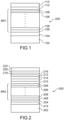
- FIG. 1 an example of a semiconductor structure 100 according to the invention comprising a stack of several layers.
- the stack comprises a substrate 102 forming the base of the stack.
- the substrate 102 is for example made of monocrystalline silicon, for example of type (111).
- the thickness of the substrate is for example between 500 ⁇ m and 2 mm.
- the substrate 102 could be made for example of sapphire, which makes it possible to avoid conduction layers at the interface between GaN and sapphire.
- the stack also includes a buffer layer 104 formed on the substrate 102.
- This buffer layer 104 serves as a nucleation layer for the growth of the other layers.
- the buffer layer comprises for example AlN and has a thickness of for example between 50 nm and 500 nm, and preferably between 200 nm and 300 nm.
- This buffer layer also has the role of insulating the substrate from the GaN layer(s) which will subsequently be formed.
- the buffer layer may comprise SiC.
- the stack also includes a superlattice SR1 formed on the buffer layer 104.
- a superlattice is a periodic multilayer structure formed by the repetition, a large number of times, of an elementary pattern comprising at least two successive chemically different layers.
- the superlattice preferably comprises at least 50 elementary patterns.
- the materials of two successive layers in the superlattice are different. For example, the values of x 1 and x 2 are different, y 1 and y 2 are different, w 1 and w 2 are different, and z 1 and z 2 are different.
- the layers 106 and 108 have thicknesses less than the critical thicknesses.
- layers 106 and 108 have very low dislocation densities.
- the critical thicknesses are equal to at most 5 nm.
- critical thickness means the thickness from which the material of a layer begins to relax and therefore resume its mesh parameter without constraint.
- the thicknesses of layers 106 and 108 are between 0.5 nm and 5 nm, and preferably less than or equal to 1 nm.
- the thickness of the pattern ie the sum of the thicknesses of layers 106 and 108, is less than or equal to 5 nm.
- the two layers can have equal or different thicknesses.
- the stack also includes an interlayer 110 formed on the superlattice SR1 capable of applying compressive stresses to a GaN layer 112 formed on the interlayer 110.
- the interlayer 110 comprises a material having a mesh parameter lower than that of GaN in order to apply sufficient compressive stresses to the GaN making it possible to produce a thick GaN layer having no cracks.
- the interlayer 110 has for example a thickness of between 5 nm and 50 nm and preferably equal to 17 nm.
- the interlayer 110 is made of AIN.
- the GaN 112 layer has, for example, a thickness of 3 ⁇ m.
- a superlattice comprising 340 repetitions of a pattern comprising a layer 106 of GaN and a layer 108 of Al 0.5 Ga 0.5 N, each layer having a thickness of 1 nm.
- the electrical resistance of the supernetwork is very high. This therefore ensures electrical insulation in the stack between the GaN layer 112 and the substrate 102.
- the function of the superlattice is not to constrain the GaN layer in compression but to ensure electrical insulation between the GaN layer, more precisely the electronic component formed on the GaN layer and the substrate.
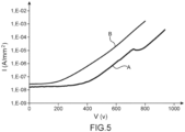
- This structure has very good voltage resistance, for example several hundred volts. Thus current leaks in the stack are significantly reduced.
- the structure can then be used in high-power electronics, for example to produce HEMT transistors (High-electron-mobility transistor in English terminology) or Schottky diodes.
- GaN layer having high crystallographic quality is obtained, i.e. having few defects.
- the electrical insulation and the application of compressive stress to the GaN layer are decorrelated, which offers greater freedom in the choice of the aluminum composition of the layers 106 and 108.
- the invention advantageously makes it possible to incorporate carbon in large quantities into the stack, which further increases the tension resistance.
- carbon can be incorporated directly into the layers of the superlattice during their formation in a manner known to those skilled in the art, for example during growth of layers 106 and 108 by phase epitaxy.
- organometallic vapor or MOCVD Metalorganic Chemical Vapor Deposition in Anglo-Saxon terminology.
- MOCVD Metalorganic Chemical Vapor Deposition in Anglo-Saxon terminology.
- the incorporation of carbon in large quantities into the superlattice does not have the effect of deteriorating the crystalline quality unlike the structures of the state of the art.
- the carbon concentration is for example equal to approximately greater than 5.10 18 .
- compositions of the layers of the patterns varying from one network to another. It can be envisaged to have compositions of the superlattices which vary in a given direction between the superlattice located closest to the substrate and that located closest to the GaN layer.
- the combination of several superlattices according to the invention further increases the tension resistance of the structure.
- the AlN interlayer can be replaced by a superlattice capable of applying a compressive stress to the GaN layer which will be produced on the superlattice.
- the compositions of the layers are chosen so that the average composition of the network is high in AlGaN, for example of the order of 80%.
- the structure 200 comprises a substrate 202, for example in Si type (111), a buffer layer 204 for example in AIN, a superlattice SR2 similar to the superlattice SR1 of the structure 100, an interlayer 210 similar to the interlayer 110, a layer 214 whose material has a mesh parameter lower than that of GaN but greater than that of the material of the interlayer 210.
- layer 214 By inserting the layer 214 between the interlayer and the GaN layer, the difference in mesh parameter between the interlayer 210 and the GaN is gradually reduced.
- the addition of layer 214 has the effect of better retaining compression in the layers, allowing the growth of a thicker GaN layer without cracking during cooling.
- layer 214 is an AlGaN layer whose thickness is for example between 50 nm and 1000 nm, preferably equal to 200 nm.
- layer 214 could be a superlattice.
- an AlGaN layer 215 is formed between the buffer layer 204 and the superlattice SR2.
- the SR2 superlattice plays the same role as an AIGaN, that is, it helps transmit compression from the AIGaN to the GaN. Additionally, the SR2 superlattice is more resistive than an AIGaN, as is the case for the SR1 superlattice.
- Layer 215 has, for example, a thickness equal to 0.5 ⁇ m.
- the structure also includes a GaN layer 216 formed on the GaN layer 212 forming a channel, an AlN layer 218, an AlGaN layer 220 and a GaN layer 222.
- the structure 200 has for example a thickness of 4.8 ⁇ m.
- the AlGaN layer 214 can be replaced by a superlattice which has the same function as the AlGaN layer 214.
- the structure 300 comprises a substrate 302 for example in Si type (111), a buffer layer 304 for example in AIN, a superlattice SR3 similar to the superlattice SR1 of structure 100, a GaN layer 324 formed on superlattice SR3, an interlayer 310 formed on layer 324, the interlayer being similar to interlayer 110, a layer 314 similar to layer 214.
- the GaN of layer 324 is a so-called 2D or 2-dimensional GaN layer, meaning that no roughness is generated, there are no “3D” islands and the surface remains flat.
- the formation of such a layer is well known to those skilled in the art.
- the production of a stack of a 2D GaN layer and an AIN layer has the advantage of revealing buried cracks at the interface between the GaN and the AIN which contribute to the compression of the GaN 312 layer.
- the AIN could be replaced by SiC, however the effect of SiC would be less than with AIN or Al x In y B z Ga w N.
- the GaN 324 layer has a thickness for example between 50 nm and 2000 nm, preferably equal to 500 nm.
- the pattern of the superlattice can include more than two layers, it can include n layers, n >_ 2, the composition of layer n can then be written AI xn Ga 1-xn N, xn belonging to the interval [ 0; 1].
- the 3214-310-314 stack could be repeated.
- the structure 400 comprises a substrate 402, a buffer layer 404 and a superlattice SR4.
- the superlattice pattern has four layers 406, 408, 426, 428.
- the materials of two successive layers in the superlattice are different .
- Each layer has a lower thickness at the critical thickness.
- the structure 400 also includes an interlayer 410 formed on the superlattice SR4, the interlayer 410 being similar to the interlayer 110, a layer 414 similar to the layer 214.
- the pattern has a thickness of less than 5 nm.
- the SR4 superlattice has a large number of patterns, preferably at least 50.
- the different layers of the semiconductor structure are produced by growth, for example by organometallic vapor phase epitaxy, in particular the layers of the superlattice(s), by chemical vapor deposition or MOCVD (Metalorganic Chemical Vapor Deposition in English terminology) or by molecular beam epitaxy or MBE (Molecular Beam Epitaxy in English terminology).
- organometallic vapor phase epitaxy in particular the layers of the superlattice(s)
- MOCVD Metalorganic Chemical Vapor Deposition in English terminology
- MBE molecular beam epitaxy in English terminology
- the typical temperature is of the order of 1000°C, a pressure of 100 mbar, under hydrogen with a partial ammonia pressure of 30 mbar
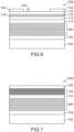
- the GaN layer 112 obtained can be used as an active layer of semiconductor devices made from the substrate formed by the structure 200.
- a HEMT transistor 300 can be made from the GaN layer 112, as represented schematically on the Figure 6 .
- This layer 112 is doped, for example with carbon and with a concentration, for example equal to approximately 10 19 cm -3 .
- An additional layer 114 comprising a semiconductor similar to that of layer 112 and thinner than layer 112 (thickness for example equal to approximately 100 nm, or between approximately 25 nm and 1 ⁇ m), and also comprising carbon in as a dopant with a concentration for example equal to approximately 5.10 16 cm -3 , is formed on layer 112.
- This additional layer 114 of GaN is intended to form the channel of the HEMT transistor 500.
- a spacer layer 116 comprising for example AlN and with a thickness equal to approximately 1 nm, is then placed on the additional layer 114 of GaN.
- a layer of AlGaN 118 comprising for example a gallium content equal to approximately 80% and making it possible to ensure the formation of a two-dimensional electron gas in the channel of the transistor 300, is formed on this spacer layer 116.
- the HEMT transistor 300 is then completed by conventional steps such as forming the source 120 and drain 122 regions, metal contacts, gate 124, etc.
- the semiconductor structure according to the invention is particularly suitable for the production of high power transistors due to the high voltage withstand, for example for the production of HEMT.
- the GaN layer 112 is used as the active layer of a light-emitting diode 600 as shown for example in the Figure 7 .
- layer 112 can be n-doped for example with silicon.
- a quantum well structure 126 comprising barrier layers of GaN and emissive layers of InGaN is then formed on layer 112.
- a layer 128 of GaN doped p, for example with magnesium, can finally be produced on the quantum well structure. 126.
- a current circulating between layers 112 and 128 causes an emission whose wavelength corresponds to the forbidden gap of the InGaN in the wells.
Landscapes
- Junction Field-Effect Transistors (AREA)
- Chemical & Material Sciences (AREA)
- Crystallography & Structural Chemistry (AREA)
- Electrodes Of Semiconductors (AREA)
Applications Claiming Priority (2)
| Application Number | Priority Date | Filing Date | Title |
|---|---|---|---|
| FR1558766A FR3041470B1 (fr) | 2015-09-17 | 2015-09-17 | Structure semi-conductrice a tenue en tension amelioree |
| EP16189001.7A EP3144956A1 (de) | 2015-09-17 | 2016-09-15 | Halbleiterstruktur mit verbesserter spannungsfestigkeit |
Related Parent Applications (1)
| Application Number | Title | Priority Date | Filing Date |
|---|---|---|---|
| EP16189001.7A Division EP3144956A1 (de) | 2015-09-17 | 2016-09-15 | Halbleiterstruktur mit verbesserter spannungsfestigkeit |
Publications (2)
| Publication Number | Publication Date |
|---|---|
| EP4336544A2 true EP4336544A2 (de) | 2024-03-13 |
| EP4336544A3 EP4336544A3 (de) | 2024-05-15 |
Family
ID=55646661
Family Applications (2)
| Application Number | Title | Priority Date | Filing Date |
|---|---|---|---|
| EP23219424.1A Pending EP4336544A3 (de) | 2015-09-17 | 2016-09-15 | Halbleiterstruktur mit verbesserter spannungsfestigkeit |
| EP16189001.7A Pending EP3144956A1 (de) | 2015-09-17 | 2016-09-15 | Halbleiterstruktur mit verbesserter spannungsfestigkeit |
Family Applications After (1)
| Application Number | Title | Priority Date | Filing Date |
|---|---|---|---|
| EP16189001.7A Pending EP3144956A1 (de) | 2015-09-17 | 2016-09-15 | Halbleiterstruktur mit verbesserter spannungsfestigkeit |
Country Status (3)
| Country | Link |
|---|---|
| US (1) | US9923061B2 (de) |
| EP (2) | EP4336544A3 (de) |
| FR (1) | FR3041470B1 (de) |
Families Citing this family (11)
| Publication number | Priority date | Publication date | Assignee | Title |
|---|---|---|---|---|
| JP6473017B2 (ja) * | 2015-03-09 | 2019-02-20 | エア・ウォーター株式会社 | 化合物半導体基板 |
| DE102016120335A1 (de) * | 2016-10-25 | 2018-04-26 | Osram Opto Semiconductors Gmbh | Halbleiterschichtenfolge und Verfahren zur Herstellung einer Halbleiterschichtenfolge |
| FR3066045A1 (fr) * | 2017-05-02 | 2018-11-09 | Commissariat A L'energie Atomique Et Aux Energies Alternatives | Diode electroluminescente comprenant des couches de conversion en longueur d'onde |
| US12289901B2 (en) | 2021-04-12 | 2025-04-29 | Innoscience (Suzhou) Technology Co., Ltd. | Semiconductor device and method for manufacturing the same |
| US12125801B2 (en) | 2021-04-12 | 2024-10-22 | Innoscience (Suzhou) Technology Co., Ltd. | Semiconductor device and method for manufacturing the same |
| US20220328678A1 (en) * | 2021-04-12 | 2022-10-13 | Innoscience (Suzhou) Technology Co., Ltd. | Semiconductor device and method for manufacturing the same |
| US12317532B2 (en) | 2021-04-12 | 2025-05-27 | Innoscience (Suzhou) Technology Co., Ltd. | Semiconductor device and method for manufacturing the same |
| US12125902B2 (en) | 2021-04-12 | 2024-10-22 | Innoscience (Suzhou) Technology Co., Ltd. | Semiconductor device and method for manufacturing the same |
| WO2022217413A1 (en) | 2021-04-12 | 2022-10-20 | Innoscience (Suzhou) Technology Co., Ltd. | Semiconductor device and method for manufacturing thereof |
| US12279444B2 (en) | 2021-04-12 | 2025-04-15 | Innoscience (Suzhou) Technology Co., Ltd. | Semiconductor device and method for manufacturing the same |
| US12274082B2 (en) | 2021-04-12 | 2025-04-08 | Innoscience (Suzhou) Technology Co., Ltd. | Semiconductor device and method for manufacturing the same |
Citations (1)
| Publication number | Priority date | Publication date | Assignee | Title |
|---|---|---|---|---|
| WO2013001014A1 (en) | 2011-06-30 | 2013-01-03 | Soitec | Method for manufacturing a thick epitaxial layer of gallium nitride on a silicon or similar substrate and layer obtained using said method |
Family Cites Families (7)
| Publication number | Priority date | Publication date | Assignee | Title |
|---|---|---|---|---|
| FR2810159B1 (fr) | 2000-06-09 | 2005-04-08 | Centre Nat Rech Scient | Couche epaisse de nitrure de gallium ou de nitrure mixte de gallium et d'un autre metal, procede de preparation, et dispositif electronique ou optoelectronique comprenant une telle couche |
| JP3569807B2 (ja) * | 2002-01-21 | 2004-09-29 | 松下電器産業株式会社 | 窒化物半導体素子の製造方法 |
| US7115896B2 (en) * | 2002-12-04 | 2006-10-03 | Emcore Corporation | Semiconductor structures for gallium nitride-based devices |
| JP5309452B2 (ja) * | 2007-02-28 | 2013-10-09 | サンケン電気株式会社 | 半導体ウエーハ及び半導体素子及び製造方法 |
| EP2498282A4 (de) * | 2009-11-04 | 2014-06-25 | Dowa Electronics Materials Co Ltd | Epitaktisch beschichtetes gruppe-iii-nitrid-substrat |
| JP5492984B2 (ja) * | 2010-04-28 | 2014-05-14 | 日本碍子株式会社 | エピタキシャル基板およびエピタキシャル基板の製造方法 |
| FR3028670B1 (fr) | 2014-11-18 | 2017-12-22 | Commissariat Energie Atomique | Structure semi-conductrice a couche de semi-conducteur du groupe iii-v ou ii-vi comprenant une structure cristalline a mailles cubiques ou hexagonales |
-
2015
- 2015-09-17 FR FR1558766A patent/FR3041470B1/fr active Active
-
2016
- 2016-09-15 US US15/266,125 patent/US9923061B2/en active Active
- 2016-09-15 EP EP23219424.1A patent/EP4336544A3/de active Pending
- 2016-09-15 EP EP16189001.7A patent/EP3144956A1/de active Pending
Patent Citations (1)
| Publication number | Priority date | Publication date | Assignee | Title |
|---|---|---|---|---|
| WO2013001014A1 (en) | 2011-06-30 | 2013-01-03 | Soitec | Method for manufacturing a thick epitaxial layer of gallium nitride on a silicon or similar substrate and layer obtained using said method |
Also Published As
| Publication number | Publication date |
|---|---|
| FR3041470A1 (fr) | 2017-03-24 |
| US9923061B2 (en) | 2018-03-20 |
| FR3041470B1 (fr) | 2017-11-17 |
| EP4336544A3 (de) | 2024-05-15 |
| EP3144956A1 (de) | 2017-03-22 |
| US20170084697A1 (en) | 2017-03-23 |
Similar Documents
| Publication | Publication Date | Title |
|---|---|---|
| EP4336544A2 (de) | Halbleiterstruktur mit verbesserter spannungsfestigkeit | |
| EP2617069B1 (de) | Nanodraht-basierte lichtemittierende vorrichtung | |
| EP3333880B1 (de) | Halbleiterstruktur mit schicht aus halbleitern der gruppe iii-v , die eine kristalline struktur aus hexagonalen gittern umfasst | |
| FR2929445A1 (fr) | Procede de fabrication d'une couche de nitrure de gallium ou de nitrure de gallium et d'aluminium | |
| FR2969995A1 (fr) | Procede de realisation d'un support comportant des nanostructures en nitrure(s) a phase zinc blende | |
| FR3080487A1 (fr) | Procede de fabrication d’un dispositif optoelectronique a matrice de diodes | |
| FR2964796A1 (fr) | Dispositif optoelectronique a base de nanofils pour l'emission de lumiere | |
| FR2924270A1 (fr) | Procede de fabrication d'un dispositif electronique | |
| FR3011981A1 (fr) | Transistor hemt a base d'heterojonction | |
| EP2697831A1 (de) | Hemt-transistoren aus (iii-b) -n-halbleitern mit grossem bandabstand und mit bor | |
| FR2997420A1 (fr) | Procede de croissance d'au moins un nanofil a partir d'une couche d'un metal de transition nitrure obtenue en deux etapes | |
| EP3117465A1 (de) | Feldeffekttransistor mit heteroübergang | |
| FR3059467A1 (fr) | Transistor a heterojonction a structure verticale | |
| EP3011603B1 (de) | Verfahren zur herstellung einer halbleiterstruktur und halbleiterkomponente mit solch einer halbleiterstruktur | |
| FR3097681A1 (fr) | Procédé de réalisation de vignettes de nitrure destinées chacune à former un dispositif électronique ou optoélectronique | |
| FR3080710A1 (fr) | Transistor hemt et procedes de fabrication favorisant une longueur et des fuites de grille reduites | |
| EP4348720B1 (de) | Optoelektronische vorrichtung und verfahren zur herstellung davon | |
| EP3440692B1 (de) | Halbleiterstruktur mit iii-n-material | |
| EP3900017B1 (de) | Verfahren zur herstellung eines wachstumssubstrats | |
| FR2891663A1 (fr) | Procede de fabrication d'un dispositif a semi-conducteur. | |
| EP3973579B1 (de) | Optoelektronische vorrichtung mit leuchtdioden, deren dotierter bereich ein äusseres segment basierend auf aluminium und galiumnitrid enthält | |
| FR3011385A1 (fr) | Diode schottky en nitrure de gallium avec anneau de garde | |
| WO2026057719A1 (fr) | Substrat intermediaire pour la fabrication d'un substrat pour transistor a haute mobilite d'electrons | |
| WO2023275471A1 (fr) | Procede de realisation de diodes electroluminescentes | |
| FR3091622A1 (fr) | Structure semi-conductrice optoélectronique comprenant une couche d’injection de type p à base d’InGaN |
Legal Events
| Date | Code | Title | Description |
|---|---|---|---|
| PUAI | Public reference made under article 153(3) epc to a published international application that has entered the european phase |
Free format text: ORIGINAL CODE: 0009012 |
|
| STAA | Information on the status of an ep patent application or granted ep patent |
Free format text: STATUS: REQUEST FOR EXAMINATION WAS MADE |
|
| 17P | Request for examination filed |
Effective date: 20231221 |
|
| AC | Divisional application: reference to earlier application |
Ref document number: 3144956 Country of ref document: EP Kind code of ref document: P |
|
| AK | Designated contracting states |
Kind code of ref document: A2 Designated state(s): AL AT BE BG CH CY CZ DE DK EE ES FI FR GB GR HR HU IE IS IT LI LT LU LV MC MK MT NL NO PL PT RO RS SE SI SK SM TR |
|
| REG | Reference to a national code |
Ref country code: DE Ref legal event code: R079 Free format text: PREVIOUS MAIN CLASS: H01L0021020000 Ipc: H01L0021200000 |
|
| PUAL | Search report despatched |
Free format text: ORIGINAL CODE: 0009013 |
|
| AK | Designated contracting states |
Kind code of ref document: A3 Designated state(s): AL AT BE BG CH CY CZ DE DK EE ES FI FR GB GR HR HU IE IS IT LI LT LU LV MC MK MT NL NO PL PT RO RS SE SI SK SM TR |
|
| RIC1 | Information provided on ipc code assigned before grant |
Ipc: H01L 21/20 20060101AFI20240411BHEP |
|
| RAP3 | Party data changed (applicant data changed or rights of an application transferred) |
Owner name: COMMISSARIAT A L'ENERGIE ATOMIQUE ET AUX ENERGIESALTERNATIVES |