EP4336651A1 - Dispositif électronique comprenant une antenne - Google Patents
Dispositif électronique comprenant une antenne Download PDFInfo
- Publication number
- EP4336651A1 EP4336651A1 EP22856098.3A EP22856098A EP4336651A1 EP 4336651 A1 EP4336651 A1 EP 4336651A1 EP 22856098 A EP22856098 A EP 22856098A EP 4336651 A1 EP4336651 A1 EP 4336651A1
- Authority
- EP
- European Patent Office
- Prior art keywords
- conductive
- housing
- conductive member
- electronic device
- conductive portion
- Prior art date
- Legal status (The legal status is an assumption and is not a legal conclusion. Google has not performed a legal analysis and makes no representation as to the accuracy of the status listed.)
- Pending
Links
Images






















Classifications
-
- H—ELECTRICITY
- H01—ELECTRIC ELEMENTS
- H01Q—ANTENNAS, i.e. RADIO AERIALS
- H01Q1/00—Details of, or arrangements associated with, antennas
- H01Q1/12—Supports; Mounting means
- H01Q1/22—Supports; Mounting means by structural association with other equipment or articles
- H01Q1/24—Supports; Mounting means by structural association with other equipment or articles with receiving set
- H01Q1/241—Supports; Mounting means by structural association with other equipment or articles with receiving set used in mobile communications, e.g. GSM
- H01Q1/242—Supports; Mounting means by structural association with other equipment or articles with receiving set used in mobile communications, e.g. GSM specially adapted for hand-held use
- H01Q1/243—Supports; Mounting means by structural association with other equipment or articles with receiving set used in mobile communications, e.g. GSM specially adapted for hand-held use with built-in antennas
-
- G—PHYSICS
- G06—COMPUTING OR CALCULATING; COUNTING
- G06F—ELECTRIC DIGITAL DATA PROCESSING
- G06F1/00—Details not covered by groups G06F3/00 - G06F13/00 and G06F21/00
- G06F1/16—Constructional details or arrangements
-
- G—PHYSICS
- G09—EDUCATION; CRYPTOGRAPHY; DISPLAY; ADVERTISING; SEALS
- G09F—DISPLAYING; ADVERTISING; SIGNS; LABELS OR NAME-PLATES; SEALS
- G09F9/00—Indicating arrangements for variable information in which the information is built-up on a support by selection or combination of individual elements
- G09F9/30—Indicating arrangements for variable information in which the information is built-up on a support by selection or combination of individual elements in which the desired character or characters are formed by combining individual elements
-
- H—ELECTRICITY
- H01—ELECTRIC ELEMENTS
- H01Q—ANTENNAS, i.e. RADIO AERIALS
- H01Q1/00—Details of, or arrangements associated with, antennas
- H01Q1/52—Means for reducing coupling between antennas; Means for reducing coupling between an antenna and another structure
- H01Q1/528—Means for reducing coupling between antennas; Means for reducing coupling between an antenna and another structure reducing the re-radiation of a support structure
-
- H—ELECTRICITY
- H01—ELECTRIC ELEMENTS
- H01Q—ANTENNAS, i.e. RADIO AERIALS
- H01Q9/00—Electrically-short antennas having dimensions not more than twice the operating wavelength and consisting of conductive active radiating elements
- H01Q9/04—Resonant antennas
- H01Q9/0407—Substantially flat resonant element parallel to ground plane, e.g. patch antenna
-
- H—ELECTRICITY
- H04—ELECTRIC COMMUNICATION TECHNIQUE
- H04M—TELEPHONIC COMMUNICATION
- H04M1/00—Substation equipment, e.g. for use by subscribers
- H04M1/02—Constructional features of telephone sets
-
- H—ELECTRICITY
- H04—ELECTRIC COMMUNICATION TECHNIQUE
- H04B—TRANSMISSION
- H04B1/00—Details of transmission systems, not covered by a single one of groups H04B3/00 - H04B13/00; Details of transmission systems not characterised by the medium used for transmission
- H04B1/38—Transceivers, i.e. devices in which transmitter and receiver form a structural unit and in which at least one part is used for functions of transmitting and receiving
- H04B1/3827—Portable transceivers
Definitions
- Various embodiments of the disclosure relate to an electronic device including an antenna.
- An electronic device may include a display to provide visual information.
- At least a portion of the housing defining the outer periphery of the electronic device may be formed of a metal frame, and. the wireless communication circuit may perform wireless communication by feeding power to at least a portion of the metal frame.
- An elastic foldable display may be disposed in the foldable display or the rollable electronic device.
- a conductive member may be provided at a position adjacent to the display in order to prevent/reduce performance degradation of the display due to electrostatic discharge.
- a conductive member may be disposed at a position adjacent to the display in order to prevent/reduce performance degradation of the display due to electrostatic discharge.
- an antenna using at least a portion of a metal frame as an antenna radiator may be deteriorated in antenna radiation performance due to interference between the conductive member and at least a portion of the metal frame used as the antenna radiator.
- the electronic device may include a split portion in the conductive member provided adjacent to the display in order to prevent performance degradation of the display due to electrostatic discharge.
- An electronic device may include: a first housing including a first edge oriented in a first direction and a second edge oriented in a second direction perpendicular to the first direction; a second housing connected to the first housing to be rotatable relative to the first housing, wherein the second housing includes a third edge corresponding to the first edge and a fourth edge corresponding to the second edge when the first housing and the second housing face each other; a flexible display defining a front surface of the electronic device and is disposed over the first housing and the second housing; a dielectric material at least partially disposed between the flexible display and the fourth edge of the second housing while at least partially surrounding a perimeter of the flexible display; a conductive member comprising a conductive material located between the dielectric material and the flexible display; and a wireless communication circuit disposed within the first housing or the second housing, wherein the fourth edge may include a first conductive portion, a first non-conductive portion, a second conductive portion, a second non-conductive portion, and a third conductive portion, the fourth edge may
- An electronic device may include: a housing including a first edge oriented in a first direction and a second edge oriented in a second direction perpendicular to the first direction; a display defining a front surface of the electronic device; a dielectric material at least partially disposed between the display and the second edge of the housing and at least partially surrounding a perimeter of the display; a conductive member comprising a conductive material located between the dielectric material and the display; and a wireless communication circuit disposed within the housing, wherein the second edge may include a first conductive portion, a second conductive portion, and a first non-conductive portion disposed between the first conductive portion and the second conductive portion, the conductive member may be provided with a first split portion to correspond to the first non-conductive portion of the second edge of the housing, and the wireless communication circuit may be configured to transmit and/or receive a radio signal using at least one of the first conductive portion and the second conductive portion of the housing.
- an electronic device is provided with a split portion in a conductive member at a position adj acent to a display in order to prevent/reduce performance deterioration of the display due to electrostatic discharge. As a result, it is possible to suppress deterioration of antenna radiation performance.
- an electronic device is provided with a protrusion on at least a portion of a conductive member disposed at a position adjacent to a display. As a result, it is possible to protect the display from electrostatic discharge.
- FIG. 1 is a perspective view of an electronic device 100 according to an embodiment.
- the electronic device 100 may include a first housing 110, a second housing 120, a connecting member 103, and/or a display 140.
- the first housing 110 and the second housing 120 may be coupled to each other via a connecting member 130 to be rotatable about a first axis (e.g., the +x-axis in FIG. 1 ) oriented in a first direction (e.g., the x-axis direction in FIG. 1 ) with respect to the first housing 110.
- the first housing 110 and the second housing 120 are illustrated with respect to a structure that is foldable about the +x-axis direction or the -x-axis direction (or the "horizontal direction"), but is not limited thereto.
- the first housing 110 and the second housing 120 may be foldable about the +y-axis direction or the - y-axis direction (or the "vertical direction").
- the rear surfaces of the first housing 110 and the second housing 120 may be covered with a rear cover (not illustrated).
- a rear cover (not illustrated).
- at least a portion of the rear cover may be formed of a non-conductive material.
- a display 140 may be disposed over the first housing 110 and the second housing 120.
- the display 140 may occupy most of the front surface of the electronic device 100.
- the display 140 may include a flexible display.
- the display 140 when the electronic device 100 is in a folded state, the display 140 may be flexibly bent depending on an angle formed between the first housing 110 and the second housing 120.
- the first housing 110 may include a first edge 110a extending in a second direction (e.g., the +y-axis direction in FIG. 1 ) and a second edge 110b extending in a first direction (e.g., the +x-axis direction in FIG. 1 ) perpendicular to the second direction (e.g., the +y-axis direction in FIG. 1 ).
- a third edge 120a corresponding to the first edge 110a and a fourth edge 120b corresponding to the second edge 110b may be included.
- the electronic device 100 may be replaced with a bar-type electronic device.
- the bar-type electronic device may include a housing in which the first housing 110 and the second housing 120 are integrally configured without including a connecting member. Accordingly, the following description of the second housing 120 may be understood as being substantially the same as a description of a housing of a bar-type electronic device.
- FIG. 2A illustrates a cross section taken along line Y-Y' of FIG. 1 in the second housing 120 according to the embodiment of FIG. 1 .
- the second housing 120 may include conductive portions 210 included in the fourth edge 120b (e.g., refer to FIG. 2B ) and a dielectric material 230 disposed between the fourth edge 120b and a bent portion 141.
- the second housing 120 may correspond to the housing of the bar-type electronic device.
- the description of the second housing 120 may be substantially applicable to the first housing 110 as it is.
- the dielectric material 230 may be disposed between the second edge 110b and the bent 141 in the first housing 110.
- a portion of the second housing 120 may include an injection-molded part 290 formed adjacent to the conductive portions 210.
- the injection-molded part 290 may be formed of a non-conductive material.
- the injection-molded part 290 may be formed of a dielectric material having a predetermined (or specified) dielectric constant.
- a conductive member (or a conductive portion) 240 may be disposed between the dielectric material 230 and the bent portion 141.
- at least a portion of the conductive member 240 may be disposed on the dielectric material 230 such that one surface of the conductive member 240 faces the inside of the second housing 120.
- the conductive member 240 may include a conductive adhesive tape or an FPCB including a conductive portion.
- the conductive member 240 may be a tape including a flexible (soft) conductive adhesive layer.
- a display circuit unit (display driver IC (DDI)) may be disposed below (e.g., in the -z axis direction) of the bent portion 141 or the display (e.g., the display 140 in FIG. 1 ).
- the display circuit unit may include a plurality of circuits and elements for driving the display.
- the conductive member 240 may protect the display circuit unit from electrostatic discharge.
- the conductive member 240 may provide a discharge path that transfers discharge occurring near the dielectric material 230 to the conductive portions 210 to prevent/reduce performance degradation of the display circuit unit.
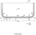
- FIG. 2B illustrates a portion of the front surface of the second housing 120 according to an embodiment.
- the fourth edge 120b of the second housing 120 may include a first conductive portion 211, a first non-conductive portion 221, a second conductive portion 212, a second non-conductive portion. 222, and/or a third conductive portion 213.
- a conductive portion may be replaceably understood as a conductive unit or a conductive region
- a non-conductive portion may be replaceably understood as a non-conductive unit or a split portion.
- the first conductive portion 211, the second conductive portion 212, or the third conductive portion 213 may include a metallic material.
- the first conductive portion 211, the second conductive portion 212, and the third conductive portion 213 may correspond to at least a portion of a metal housing.
- the first non-conductive portion 221 or the second non-conductive portion 222 may be formed of a dielectric material having a predetermined dielectric constant.
- the first non-conductive portion 221 and the second non-conductive portion 222 may be filled with a dielectric material.
- the wireless communication circuit (not illustrated) disposed within the first housing 110 or the second housing 120 may transmit/receive a radio signal by using at least one of the first conductive portion 211 or the second conductive portion 212.
- a wireless communication circuit disposed on a printed circuit board within the second housing 120 may transmit and/or receive a radio signal by feeding power to at least one of the first conductive portion 211, the second conductive portion 212, or the third conductive portion.
- the conductive member 240 may be disposed to be electrically separated from the first conductive portion 211, the second conductive portion 212, or the third conductive portion 213.
- the conductive member 240 may include a first conductive member portion 240-1, a first split portion 241, a second conductive member portion 240-2, a second split portion 242, and/or a third conductive member portion 240-3.
- the first conductive member portion 240-1, the second conductive member portion 240-2, and the third conductive member portion 240-3 may include a conductive material.
- the first conductive member portion 240-1, the second conductive member portion 240-2, and the third conductive member portion 240-3 may be formed of a conductive tape.
- the first split portion 241 and the second split portion 242 may include a non-conductive material.
- the first split portion 241 or the second split portion 242 may be filled with a dielectric material having a predetermined dielectric constant.
- first split portion 241 may be disposed to correspond to the first non-conductive portion 221.
- second split portion 242 may be disposed to correspond to the second non-conductive portion 222.
- first split portion 241 may be provided at a point of the conductive member 240 to face the first non-conductive portion 221
- the second split portion 242 may be provided at another point of the conductive member 240 to face the second non-conductive portion 222.
- the conductive member 240 may be provided with the first split portion 241 without being provided with the second split portion 242.
- the conductive member 240 may be provided with the second split portion 242 without being provided with the first split portion 241.
- FIG. 3 illustrates graphs each showing the total radiation efficiency of an electronic device 100 according to whether the split portions 241 and 242 are provided in the conductive member 240 according to an embodiment.
- the radiation efficiency in a predetermined band may be improved (or deterioration of the total radiation efficiency is suppressed) compared to the case in which the split portions 241 and 242 are not provided in the conductive portion.
- the first conductive portion 211 may operate as an antenna radiator in a high-frequency band (e.g., about 2.2 GHz to about 3.2 GHz (a high band)), and the second conductive portion 212 may operate as an antenna radiator in an intermediate frequency band (e.g., a frequency band of about 1.4 GHz to about 2 GHz (a mid-band)).
- a high-frequency band e.g., about 2.2 GHz to about 3.2 GHz (a high band)
- an intermediate frequency band e.g., a frequency band of about 1.4 GHz to about 2 GHz (a mid-band)
- the disclosure is not limited to the case in which only a portion of any of the first conductive portion 211, the second conductive portion 212, or the third conductive portion 213 operates as an antenna radiator.
- the first conductive portion 211, the second conductive portion 212, and the third conductive portion 213 may each receive power from the wireless communication circuit and operate as an antenna radiator in a predetermined frequency band.
- the third conductive portion 213 may receive power from the wireless communication circuit and operate as an antenna radiator in a designated frequency band.
- the total antenna radiation efficiency via the first conductive portion 211 or the second conductive portion 212 may be improved in the frequency band of about 2.5 GHz to about 2.5 GHz compared to the case in which the split portions 241 and 242 are not provided in the conductive member 240.
- the antenna radiation efficiency may be improved (or the deterioration of the total radiation efficiency is suppressed) in the frequency band of about 2 GHz or more.
- the total antenna radiation efficiency via the second conductive portion 212 or the third conductive portion 213 may be improved in the frequency band of about 1.4 GHz to about 1.8 GHz compared to the case in which the split portions 241 and 242 are not provided in the conductive member 240.
- the antenna radiation efficiency may be improved in the frequency band of about 2 GHz or less.
- FIG. 4A illustrates an electric field distribution formed in the second housing 120 when the conductive member 240a in which split portions according to an embodiment are absent is provided.
- the conductive member 240a in which split portions are absent may include a first conductive portion 241a and a second conductive portion 242a.
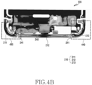
- FIG. 4B illustrates an electric field distribution formed in the second housing when the conductive member 240 in which split portions according to an embodiment are present is provided.
- the conductive member 240 in which the split portions are present may include a first split portion 241 and a second split portion 242.
- the electric fields of the conductive portions 210 are coupled to the conductive member 240 so that an electric field is also capable of being formed in the conductive member 240.
- the antenna radiation performance through the conductive portions 210 may be deteriorated.
- the same electric field distribution as those in the first region 410 and the second region 420 may be formed.
- the conductive member 240a may include a first conductive portion 241a and a second conductive portion 242a without including a non-conductive portion.
- an electric field is also formed in the conductive member 240a, so that parasitic resonance may occur, which may cause the antenna radiation performance of the electronic device 100 to be deteriorated.
- the same electric field distribution as those in the third region 430 and the fourth region 440 may be formed.
- the conductive member 240a in which split portions are absent is disposed in the second housing 120
- the conductive member 240 in which split portions are present is disposed in the second housing 120, since the amount of coupling to the conductive member 240 is reduced, parasitic resonance may be weakened or eliminated.
- FIG. 5 illustrates graphs each showing the total radiation efficiency of the electronic device 100 according to the number of split portions provided in the conductive member 240 according to an embodiment.
- the total radiation efficiency of the electronic device 100 may vary depending on the number of split portions provided in the conductive member 240.
- the total radiation efficiency of the electronic device 100 may be improved in the frequency band of about 1.65 GHz to about 2.3 GHz compared to the case in which split portions are absent in the conductive member 240.
- parasitic resonance occurs in the frequency band of about 1.6 GHz to about 1.7 GHz, and thus the total radiation efficiency of the electronic device 100 may be reduced (or deteriorated).
- FIG. 6 illustrates graphs each showing the total radiation efficiency of the electronic device 100 when the length of the conductive member 240 is changed according to an embodiment.
- the region in which the first split portion 241 and the second split portion 242 overlap each other increases.
- the frequency of parasitic resonance shifts from a frequency band of about 1.9 GHz to a frequency band of about 1.6 GHz, the parasitic resonance may act as a parasitic component which may cause the total radiation performance to be deteriorated in a predetermined band.
- the length of the conductive member 240 is the same as the length of the second conductive portion 212
- parasitic resonance may occur in the frequency band of about 1 GHz to about 2 GHz, which may cause the total antenna radiation performance to be deteriorated.
- the total radiation efficiency of the electronic device 100 may not be significantly affected in the frequency band of about 2 GHz or higher.
- FIG. 7 illustrates graphs each showing a total antenna radiation efficiency depending on whether the split portions 241 and 242 provided in the conductive member 240 according to an embodiment and the non-conductive portions 221 and 222 provided in the second housing 120 are aligned.
- the total antenna radiation efficiency in a predetermined band may vary depending on whether the first split portion 241 and the first non-conductive portion 221 are aligned and whether the second split portion 242 and the second non-conductive portion 222 are aligned.
- the total antenna radiation performance may be deteriorated in the frequency band of about 600 MHz to about 950 MHz, a frequency band of about 1.7 GHz to about 2.5 GHz, or a frequency band of about 4 GHz to about 5.4 GHz.
- the total radiation efficiency may decrease by about 0.5 dB to about 1.0 dB in the frequency band of about 600 MHz to about 950 MHz.
- the total radiation efficiency may decrease by about 0.5 dB to about 1.0 dB in the frequency band of about 1.7 GHz to about 2.5 GHz.
- the total radiation efficiency may decrease by about 0.5 dB in the frequency band of about 4 GHz to about 5.4 GHz.
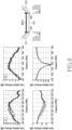
- FIG. 8A illustrates graphs each showing the total radiation efficiency of the electronic device 100 according to the lengths/widths of the split portions 241 and 242 included in the conductive member 240 according to an embodiment.
- FIG. 8B illustrates graphs each showing the total radiation efficiency of the electronic device according to an overlapping degree between a split portion of a conductive member and a non-conductive portion of a housing according to an embodiment.
- the total radiation efficiency by the electronic device 100 may be improved.
- the total antenna radiation performance may be improved in the frequency band of about 1.6 GHz to about 1.8 GHz.
- the total antenna radiation performance may be improved in the frequency band of about 2.4 GHz to about 2.7 GHz.
- the conductive member 240 may be disposed such that the first split portion 241 included in the conductive member 240 at least partially overlaps the first non-conductive portion 221 of the housing 110 or 120.
- the total antenna radiation efficiency of the electronic device 100 may be improved.
- the total antenna radiation efficiency may be improved in the frequency band of about 1.6 GHz to about 1.8 GHz.
- the total antenna radiation efficiency may be improved in the frequency band of about 1.6 GHz to about 1.8 GHz.
- FIG. 9A illustrates a conductive member 240 according to an embodiment.
- FIG. 9B illustrates a cross section of a portion of the electronic device 100 including the conductive member 240 according to the embodiment of FIG. 9A when the conductive member 240 is cut along line A-A'.
- FIG. 9C illustrates a cross section of a portion of the electronic device 100 when the conductive member 240 according to the embodiment of FIG. 9A is cut along line B-B'.
- the second conductive member portion 240-2 may include at least one first protrusion 910.
- the second conductive member portion 240-2 may be spaced apart from the second conductive portion 212 by a predetermined distance in the region A-A'.
- the first protrusion 910 included in the second conductive member portion 240-2 in the region B-B' may extend from the second conductive member portion 240-2 to at least partially face the second conductive portion 212.
- at least a portion of the first protrusion 910 may be disposed between the second conductive portion 212 and a display circuit unit.
- the first protrusion 910 may provide a discharge path such that discharge occurring at a position adjacent to the second conductive member portion 240-2 flows to the second conductive portion 212.
- the first protrusion 910 may prevent electrostatic discharge more effectively.
- FIG. 10A illustrates a conductive member 240 according to an embodiment.
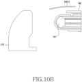
- FIG. 10B illustrates a cross section of a portion of the electronic device 100 when the conductive member 240 according to the embodiment of FIG. 10A is cut along line C-C'.
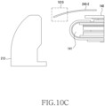
- FIG. 10C illustrates a cross section of a portion of the electronic device 100 when the conductive member 240 according to the embodiment of FIG. 10A is cut along line D-D'.
- the second conductive member portion 240-2 may include at least one first protrusion 1010.
- the second conductive member portion 240-2 may be spaced apart from the second conductive portion 212 by a predetermined distance in the region C-C'.
- the second protrusion 1010 included in the second conductive member portion 240-2 may extend from the second conductive member portion 240-2 toward the second conductive portion 212 to be adjacent to the second conductive member portion 212.
- the second protrusion 1010 may extend seamlessly from the second conductive member portion 240-2.
- the second protrusion 1010 may provide a discharge path such that discharge occurring at a position adjacent to the second conductive member portion 240-2 flows to the second conductive portion 212.
- the second protrusion 1010 may prevent electrostatic discharge more effectively.
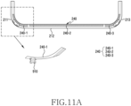
- FIG. 11A illustrates a portion of the second housing 120 when one first protrusion 910 is provided on the first conductive member portion 240-1 and/or a third conductive member portion 240-3 according to an embodiment.
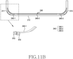
- FIG. 11B illustrates a portion of the second housing 120 when at least two first protrusions 910 are provided on the first conductive member portion 240-1 and/or the third conductive member portion 240-3 according to an embodiment.
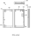
- FIG. 11C illustrates a portion of the second housing 120 when at least four first protrusions 910 are provided on the first conductive member portion 240-1 and/or the third conductive member portion 240-3 according to an embodiment.
- At least one first protrusion 910 may be provided on the first conductive member portion 240-1 and/or the third conductive member portion 240-3.
- at least one second protrusion 1010 may be provided on the first conductive member portion 240-1 and/or the third conductive member portion 240-3.
- one first protrusion 910 may be provided on each of the first conductive member portion 240-1 and/or the third conductive member portion 240-3.
- one first protrusion 910 may be provided on the first conductive member portion 240-1, and two or more first protrusions 910 may be provided on the third conductive member portion 240-3.
- two first protrusions 910 may be provided on each of the first conductive member portion 240-1 and/or the third conductive member portion 240-3.
- two first protrusions 910 may be provided on the first conductive member portion 240-1, and four first protrusions 910 may be provided on the third conductive member portion 240-3.
- first protrusions 910 may be provided in each of the first conductive member portion 240-1 and/or the third conductive member portion 240-3.
- At least one first protrusion 910 provided on the first conductive member portion 240-1 may provide a discharge path such that discharge occurring at a position adjacent to the second conductive member portion 240-1 flows to the first conductive portion 211.
- the at least one first protrusion 910 provided on the first conductive member portion 240-1 may prevent/reduce electrostatic discharge more effectively.
- At least one first protrusion 910 provided on the first conductive member portion 240-3 may provide a discharge path such that discharge occurring at a position adjacent to the third conductive member portion 240-3 flows to the third conductive portion 213.
- the at least one first protrusion 910 provided on the third conductive member portion 240-3 may prevent/reduce electrostatic discharge more effectively.
- FIG. 12 illustrates a discharge path provided along at least a portion of the dielectric material 230 and the conductive portions 210 depending on whether the conductive portion 240 including a first portion 910 or the conductive portion 240 including a second protrusion 1010 is provided.
- a discharge path for static electricity generated near the dielectric material 230 may be provided along the conductive member 240 and at least some of the conductive portions 210, rather than being formed to be directed to the display circuit unit. As a result, it is possible to prevent or suppress performance deterioration of the display 140.
- a first discharge path 1210 in which electrostatic discharge occurring near the dielectric material 230 is directed toward the display circuit unit may be provided.
- the performance of the display 140 may be deteriorated.
- a second discharge path 1220 may be provided such that electrostatic discharge occurring near the dielectric material 230 flows along the conductive member 240 and at least some of the conductive portions 210, rather than flowing to the display circuit unit.
- a discharge path of static electricity is provided along the conductive member 240 and at least some of the conductive portions 210, degradation in performance of the display 140 due to static discharge may be prevented or suppressed.
- a third discharge path 1230 may be provided such that electrostatic discharge occurring near the dielectric material 230 flows along the conductive member 240 and at least some of the conductive portions 210, rather than flowing to the display circuit unit.
- a discharge path of static electricity is provided along the conductive member 240 and at least some of the conductive portions 210, degradation in performance of the display 140 due to static discharge may be prevented or suppressed.
- FIG. 13A illustrates an electronic device 100 in which feeding points P1 and P2 and ground points G1 and G2 are provided according to an embodiment.
- FIG. 13B illustrates an electric field distribution formed in the electronic device 100 according to the embodiment of FIG. 13A .
- At least one first protrusion 910 may be provided at a position spaced apart from the feeding points P1 and P2 having a high electric field strength by a predetermined distance.
- the second protrusion 1010 may be provided at a position spaced apart from the feeding points P1 and P2 having a high electric field strength by a predetermined distance.
- a first feeding point P1 may be provided at one point of the second conductive portion 212, and a first ground point G1 may be provided at another point of the second conductive portion 212.
- a second feeding point P2 may be provided at one point of the third conductive portion 213, and a second ground point G2 may be provided at another point of the third conductive portion 213.
- the at least one first protrusion 910 provided on the second conductive member portion 240-2 may be provided at one point of the second conductive member portion 240-2 to be spaced apart from the first feeding point P1. This makes it possible for the discharge path of the first protrusion 910 provided on the second conductive member portion 240-2 to reduce the influence of the first feeding point P1.
- the first protrusion 910 provided on the third conductive member portion 240-3 may be provided at one point of the third conductive member portion 240-3 to be spaced apart from the second feeding point P2. This makes it possible for the discharge path of the first protrusion 910 provided on the third conductive member portion 240-2 not to be affected by the second feeding point P2.
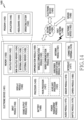
- FIG. 14 is a block diagram of an electronic device in a network environment, according to various embodiments.
- the electronic device 1401 in the network environment 1400 may communicate with an electronic device 1402 via a first network 1498 (e.g., a short-range wireless communication network), or at least one of an electronic device 1404 or a server 1408 via a second network 1499 (e.g., a long-range wireless communication network).
- a first network 1498 e.g., a short-range wireless communication network
- a second network 1499 e.g., a long-range wireless communication network
- the electronic device 1401 may communicate with the electronic device 1404 via the server 1408.
- the electronic device 1401 may include a processor 1420, memory 1430, an input module 1450, a sound output module 1455, a display module 1460, an audio module 1470, a sensor module 1476, an interface 1477, a connecting terminal 1478, a haptic module 1479, a camera module 1480, a power management module 1488, a battery 1489, a communication module 1490, a subscriber identification module(SIM) 1496, or an antenna module 1497.
- at least one of the components e.g., the connecting terminal 1478
- some of the components e.g., the sensor module 1476, the camera module 1480, or the antenna module 1497) may be implemented as a single component (e.g., the display module 1460).
- the processor 1420 may execute, for example, software (e.g., a program 1440) to control at least one other component (e.g., a hardware or software component) of the electronic device 1401 coupled with the processor 1420, and may perform various data processing or computation. According to one embodiment, as at least part of the data processing or computation, the processor 1420 may store a command or data received from another component (e.g., the sensor module 1476 or the communication module 1490) in volatile memory 1432, process the command or the data stored in the volatile memory 1432, and store resulting data in non-volatile memory 1434.
- software e.g., a program 1440
- the processor 1420 may store a command or data received from another component (e.g., the sensor module 1476 or the communication module 1490) in volatile memory 1432, process the command or the data stored in the volatile memory 1432, and store resulting data in non-volatile memory 1434.
- the processor 1420 may include a main processor 1421 (e.g., a central processing unit (CPU) or an application processor (AP)), or an auxiliary processor 1423 (e.g., a graphics processing unit (GPU), a neural processing unit (NPU), an image signal processor (ISP), a sensor hub processor, or a communication processor (CP)) that is operable independently from, or in conjunction with, the main processor 1421.
- a main processor 1421 e.g., a central processing unit (CPU) or an application processor (AP)
- auxiliary processor 1423 e.g., a graphics processing unit (GPU), a neural processing unit (NPU), an image signal processor (ISP), a sensor hub processor, or a communication processor (CP)
- the auxiliary processor 1423 may be adapted to consume less power than the main processor 1421, or to be specific to a specified function.
- the auxiliary processor 1423 may be implemented as separate from, or as part of the main processor 1421.
- the auxiliary processor 1423 may control at least some of functions or states related to at least one component (e.g., the display module 1460, the sensor module 1476, or the communication module 1490) among the components of the electronic device 1401, instead of the main processor 1421 while the main processor 1421 is in an inactive (e.g., sleep) state, or together with the main processor 1421 while the main processor 1421 is in an active state (e.g., executing an application).
- the auxiliary processor 1423 e.g., an image signal processor or a communication processor
- the auxiliary processor 1423 may include a hardware structure specified for artificial intelligence model processing.
- An artificial intelligence model may be generated by machine learning. Such learning may be performed, e.g., by the electronic device 1401 where the artificial intelligence is performed or via a separate server (e.g., the server 1408). Learning algorithms may include, but are not limited to, e.g., supervised learning, unsupervised learning, semi-supervised learning, or reinforcement learning.
- the artificial intelligence model may include a plurality of artificial neural network layers.
- the artificial neural network may be a deep neural network (DNN), a convolutional neural network (CNN), a recurrent neural network (RNN), a restricted boltzmann machine (RBM), a deep belief network (DBN), a bidirectional recurrent deep neural network (BRDNN), deep Q-network or a combination of two or more thereof but is not limited thereto.
- the artificial intelligence model may, additionally or alternatively, include a software structure other than the hardware structure.
- the memory 1430 may store various data used by at least one component (e.g., the processor 1420 or the sensor module 1476) of the electronic device 1401.
- the various data may include, for example, software (e.g., the program 1440) and input data or output data for a command related thererto.
- the memory 1430 may include the volatile memory 1432 or the non-volatile memory 1434.
- the program 1440 may be stored in the memory 1430 as software, and may include, for example, an operating system (OS) 1442, middleware 1444, or an application 1446.
- OS operating system
- middleware middleware
- application application
- the input module 1450 may receive a command or data to be used by another component (e.g., the processor 1420) of the electronic device 1401, from the outside (e.g., a user) of the electronic device 1401.
- the input module 1450 may include, for example, a microphone, a mouse, a keyboard, a key (e.g., a button), or a digital pen (e.g., a stylus pen).
- the sound output module 1455 may output sound signals to the outside of the electronic device 1401.
- the sound output module 1455 may include, for example, a speaker or a receiver.
- the speaker may be used for general purposes, such as playing multimedia or playing record.
- the receiver may be used for receiving incoming calls. According to an embodiment, the receiver may be implemented as separate from, or as part of the speaker.
- the display module 1460 may visually provide information to the outside (e.g., a user) of the electronic device 1401.
- the display module 1460 may include, for example, a display, a hologram device, or a projector and control circuitry to control a corresponding one of the display, hologram device, and projector.
- the display module 1460 may include a touch sensor adapted to detect a touch, or a pressure sensor adapted to measure the intensity of force incurred by the touch.
- the audio module 1470 may convert a sound into an electrical signal and vice versa. According to an embodiment, the audio module 1470 may obtain the sound via the input module 1450, or output the sound via the sound output module 1455 or a headphone of an external electronic device (e.g., an electronic device 1402) directly (e.g., wiredly) or wirelessly coupled with the electronic device 1401.
- an external electronic device e.g., an electronic device 1402 directly (e.g., wiredly) or wirelessly coupled with the electronic device 1401.
- the sensor module 1476 may detect an operational state (e.g., power or temperature) of the electronic device 1401 or an environmental state (e.g., a state of a user) external to the electronic device 1401, and then generate an electrical signal or data value corresponding to the detected state.
- the sensor module 1476 may include, for example, a gesture sensor, a gyro sensor, an atmospheric pressure sensor, a magnetic sensor, an acceleration sensor, a grip sensor, a proximity sensor, a color sensor, an infrared (IR) sensor, a biometric sensor, a temperature sensor, a humidity sensor, or an illuminance sensor.
- the interface 1477 may support one or more specified protocols to be used for the electronic device 1401 to be coupled with the external electronic device (e.g., the electronic device 1402) directly (e.g., wiredly) or wirelessly.
- the interface 1477 may include, for example, a high definition multimedia interface (HDMI), a universal serial bus (USB) interface, a secure digital (SD) card interface, or an audio interface.
- HDMI high definition multimedia interface
- USB universal serial bus
- SD secure digital
- a connecting terminal 1478 may include a connector via which the electronic device 1401 may be physically connected with the external electronic device (e.g., the electronic device 1402).
- the connecting terminal 1478 may include, for example, a HDMI connector, a USB connector, a SD card connector, or an audio connector (e.g., a headphone connector).
- the haptic module 1479 may convert an electrical signal into a mechanical stimulus (e.g., a vibration or a movement) or electrical stimulus which may be recognized by a user via his tactile sensation or kinesthetic sensation.
- the haptic module 1479 may include, for example, a motor, a piezoelectric element, or an electric stimulator.
- the camera module 1480 may capture a still image or moving images.
- the camera module 1480 may include one or more lenses, image sensors, image signal processors, or flashes.
- the power management module 1488 may manage power supplied to the electronic device 1401. According to one embodiment, the power management module 1488 may be implemented as at least part of, for example, a power management integrated circuit (PMIC).
- PMIC power management integrated circuit
- the battery 1489 may supply power to at least one component of the electronic device 1401.
- the battery 1489 may include, for example, a primary cell which is not rechargeable, a secondary cell which is rechargeable, or a fuel cell.
- the communication module 1490 may support establishing a direct (e.g., wired) communication channel or a wireless communication channel between the electronic device 1401 and the external electronic device (e.g., the electronic device 1402, the electronic device 1404, or the server 1408) and performing communication via the established communication channel.
- the communication module 1490 may include one or more communication processors that are operable independently from the processor 1420 (e.g., the application processor (AP)) and supports a direct (e.g., wired) communication or a wireless communication.
- AP application processor
- the communication module 1490 may include a wireless communication module 1492 (e.g., a cellular communication module, a short-range wireless communication module, or a global navigation satellite system (GNSS) communication module) or a wired communication module 1494 (e.g., a local area network (LAN) communication module or a power line communication (PLC) module).
- a wireless communication module 1492 e.g., a cellular communication module, a short-range wireless communication module, or a global navigation satellite system (GNSS) communication module
- GNSS global navigation satellite system
- wired communication module 1494 e.g., a local area network (LAN) communication module or a power line communication (PLC) module.
- LAN local area network
- PLC power line communication
- a corresponding one of these communication modules may communicate with the external electronic device via the first network 1498 (e.g., a short-range communication network, such as BluetoothTM, wireless-fidelity (Wi-Fi) direct, or infrared data association (IrDA)) or the second network 1499 (e.g., a long-range communication network, such as a legacy cellular network, a 5G network, a next-generation communication network, the Internet, or a computer network (e.g., LAN or wide area network (WAN)).
- first network 1498 e.g., a short-range communication network, such as BluetoothTM, wireless-fidelity (Wi-Fi) direct, or infrared data association (IrDA)
- the second network 1499 e.g., a long-range communication network, such as a legacy cellular network, a 5G network, a next-generation communication network, the Internet, or a computer network (e.g., LAN or wide area network (WAN)).
- the wireless communication module 1492 may identify and authenticate the electronic device 1401 in a communication network, such as the first network 1498 or the second network 1499, using subscriber information (e.g., international mobile subscriber identity (IMSI)) stored in the subscriber identification module 1496.
- subscriber information e.g., international mobile subscriber identity (IMSI)
- the wireless communication module 1492 may support a 5G network, after a 4G network, and next-generation communication technology, e.g., new radio (NR) access technology.
- the NR access technology may support enhanced mobile broadband (eMBB), massive machine type communications (mMTC), or ultra-reliable and low-latency communications (URLLC).
- eMBB enhanced mobile broadband
- mMTC massive machine type communications
- URLLC ultra-reliable and low-latency communications
- the wireless communication module 1492 may support a high-frequency band (e.g., the mmWave band) to achieve, e.g., a high data transmission rate.
- the wireless communication module 1492 may support various technologies for securing performance on a high-frequency band, such as, e.g., beamforming, massive multiple-input and multiple-output (massive MIMO), full dimensional MIMO (FD-MIMO), array antenna, analog beam-forming, or large scale antenna.
- the wireless communication module 1492 may support various requirements specified in the electronic device 1401, an external electronic device (e.g., the electronic device 1404), or a network system (e.g., the second network 1499).
- the wireless communication module 1492 may support a peak data rate (e.g., 20Gbps or more) for implementing eMBB, loss coverage (e.g., 1464dB or less) for implementing mMTC, or U-plane latency (e.g., 0.5ms or less for each of downlink (DL) and uplink (UL), or a round trip of 14ms or less) for implementing URLLC.
- a peak data rate e.g., 20Gbps or more
- loss coverage e.g., 1464dB or less
- U-plane latency e.g., 0.5ms or less for each of downlink (DL) and uplink (UL), or a round trip of 14ms or less
- the antenna module 1497 may transmit or receive a signal or power to or from the outside (e.g., the external electronic device) of the electronic device 1401.
- the antenna module 1497 may include an antenna including a radiating element composed of a conductive material or a conductive pattern formed in or on a substrate (e.g., a printed circuit board (PCB)).
- the antenna module 1497 may include a plurality of antennas (e.g., array antennas). In such a case, at least one antenna appropriate for a communication scheme used in the communication network, such as the first network 1498 or the second network 1499, may be selected, for example, by the communication module 1490 (e.g., the wireless communication module 1492) from the plurality of antennas.
- the communication module 1490 e.g., the wireless communication module 1492
- the signal or the power may then be transmitted or received between the communication module 1490 and the external electronic device via the selected at least one antenna.
- another component e.g., a radio frequency integrated circuit (RFIC)
- RFIC radio frequency integrated circuit
- the antenna module 1497 may form a mmWave antenna module.
- the mmWave antenna module may include a printed circuit board, a RFIC disposed on a first surface (e.g., the bottom surface) of the printed circuit board, or adjacent to the first surface and capable of supporting a designated high-frequency band (e.g., the mmWave band), and a plurality of antennas (e.g., array antennas) disposed on a second surface (e.g., the top or a side surface) of the printed circuit board, or adjacent to the second surface and capable of transmitting or receiving signals of the designated high-frequency band.
- a RFIC disposed on a first surface (e.g., the bottom surface) of the printed circuit board, or adjacent to the first surface and capable of supporting a designated high-frequency band (e.g., the mmWave band)
- a plurality of antennas e.g., array antennas
- At least some of the above-described components may be coupled mutually and communicate signals (e.g., commands or data) therebetween via an inter-peripheral communication scheme (e.g., a bus, general purpose input and output (GPIO), serial peripheral interface (SPI), or mobile industry processor interface (MIPI)).
- an inter-peripheral communication scheme e.g., a bus, general purpose input and output (GPIO), serial peripheral interface (SPI), or mobile industry processor interface (MIPI)
- commands or data may be transmitted or received between the electronic device 1401 and the external electronic device 1404 via the server 1408 coupled with the second network 1499.
- Each of the electronic devices 1402 or 1404 may be a device of a same type as, or a different type, from the electronic device 1401.
- all or some of operations to be executed at the electronic device 1401 may be executed at one or more of the external electronic devices 1402, 1404, or 1408.
- the electronic device 1401 instead of, or in addition to, executing the function or the service, may request the one or more external electronic devices to perform at least part of the function or the service.
- the one or more external electronic devices receiving the request may perform the at least part of the function or the service requested, or an additional function or an additional service related to the request, and transfer an outcome of the performing to the electronic device 1401.
- the electronic device 1401 may provide the outcome, with or without further processing of the outcome, as at least part of a reply to the request.
- a cloud computing, distributed computing, mobile edge computing (MEC), or client-server computing technology may be used, for example.
- the electronic device 1401 may provide ultra low-latency services using, e.g., distributed computing or mobile edge computing.
- the external electronic device 1404 may include an internet-of-things (IoT) device.
- the server 1408 may be an intelligent server using machine learning and/or a neural network.
- the external electronic device 1404 or the server 1408 may be included in the second network 1499.
- the electronic device 1401 may be applied to intelligent services (e.g., smart home, smart city, smart car, or healthcare) based on 5G communication technology or IoT-related technology.
- FIG. 15 illustrates an exploded perspective view of an electronic device including a flexible display and a conductive member according to another embodiment.
- the electronic device 1500 may include a first housing 1510, a second housing 1520, a second housing 1540, a connecting member 1550, a dielectric material 1530 and/or a display circuit unit 1541.
- the first housing 1510 and the second housing 1520 may be coupled to each other via a connecting member to be rotatable about a first axis (e.g., the y axis in FIG. 15 ) oriented in a first direction (e.g., the +y-axis direction in FIG. 15 ) with respect to the first housing 1510.
- a first axis e.g., the y axis in FIG. 15
- a first direction e.g., the +y-axis direction in FIG. 15
- the rear surfaces of the first housing 1510 and the second housing 1520 may be covered with a rear cover (not illustrated).
- a rear cover may be formed of a non-conductive material.
- a display 1540 may be disposed over the first housing 1510 and the second housing 1520.
- the display 1540 may occupy most of the front surface of the electronic device 100.
- the display 1540 may have a horizontal length W1 longer than a vertical length H1, but is not limited thereto.
- the display 1540 may include a flexible display.
- the display 1540 when the electronic device 1500 is in a folded state, the display 1540 may be flexibly bent depending on an angle formed between the first housing 1510 and the second housing 1520.
- the first housing 1510 may include a first edge 1510a extending in a second direction (e.g., the +x-axis direction in FIG. 1 ) and a second edge 1510b extending in a first direction (e.g., the +y-axis direction in FIG. 1 ) perpendicular to the second direction (e.g., the +x-axis direction in FIG. 1 ).
- the dielectric material 1530 may define at least a portion of the first housing 1510 or the exterior of the electronic device 1500.
- the dielectric material 1530 may be referred to as a decoration that defines a portion of the exterior of the electronic device 1500.
- the conductive member 1550 may be disposed between the dielectric material 1530 and the display circuit unit 1541.
- the conductive member 1550 may include a first conductive member portion 1551, a first split portion 1561, a second conductive member portion 1552, a second split portion 1562, and/or a third conductive member portion 1553.
- the first conductive member portion 1551, the second conductive member portion 1552, and the third conductive member portion 1553 may include a conductive material.
- the first conductive member portion 1551, the second conductive member portion 1552, and the third conductive member portion 1553 may be formed of a conductive tape.
- the first conductive member portion 1551, the second conductive member portion 1552, and the third conductive member portion 1553 may be provided through at least one of deposition on a dielectric material, deposition on a separate support member on the display circuitry 1541, a flexible printed circuit board (FPCB), plating, or stainless use steel (SUS).
- FPCB flexible printed circuit board
- SUS stainless use steel
- the first split portion 1561 and/or the second split portion 1562 may include a non-conductive material.
- the first split portion 1561 or the second split portion 1562 may be filled with a dielectric material having a predetermined dielectric constant.
- the first split portion 1561 may be disposed to correspond to the first non-conductive portion 1521.
- at least a portion of the second split portion 1562 may be disposed to correspond to the second non-conductive portion 1522.
- the first split portion 1561 may be provided at a point of the conductive member 1550 to face the first non-conductive portion 1521, and the second split portion 1562 may be provided at another point of the conductive member 1550 to face the second non-conductive portion 1522.
- the conductive member 1550 may be provided with the first split portion 1561 without being provided with the second split portion 1562.
- the conductive member 1550 may be provided with the second split portion 1562 without being provided with the first split portion 1561.
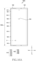
- FIG. 16A illustrates a first state of an electronic device including a rollable display according to an embodiment.
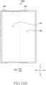
- FIG. 16B illustrates a second state of the electronic device including a rollable display according to an embodiment.
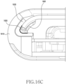
- FIG. 16C illustrates a cross section taken along axis E-E' in the electronic device according to the embodiment of FIG. 16A .
- the display 1640 may be placed on one surface of the electronic device 1600 according to an embodiment.
- the surface on which the display 1640 is placed will be referred to as a front surface.
- the display 1640 may occupy most of the front surface of the electronic device 1600.
- the display 1640 may have a flat shape and a curved shape.
- the display 1640 and housings 1601 and 1602, which surround at least portion of the display 1640 may be disposed on the front surface of the electronic device 1600.
- the housings 1601 and 1602 may define a partial region of the front surface, the side surface, and the rear surface of the electronic device 1600.
- the housings 1601 and 1602 may form a partial region of the side surface and the rear surface of the electronic device 1600.
- the housings 1601 and 1602 may include a first housing 1601 and a second housing 1602 that is movable relative to the first housing 1601.
- the display 1640 may include a first portion 1641 that is capable of being coupled to the second housing 1602 and a second portion 1642 that is capable of extending from the first portion 1641 and capable of being retracted into the inside of the electronic device 1600.
- the second portion 1642 of the display 1640 when the electronic device 1600 is switched from the first state 1600a to a second state 1600b according to the movement of the second housing 1602, the second portion 1642 of the display 1640 is capable of being drawn out from the inside to the outside of the electronic device 1600.
- the second portion 1642 of the display 1640 is capable of being retracted into the inside of the electronic device 1600.
- the fourth edge 1620b of the second housing 1602 may include a first conductive portion 1611, a first non-conductive portion 1621, a second conductive portion 1612, a second non-conductive portion 1622, a third conductive portion 1613, a third non-conductive portion 1623, a fourth conductive portion 1614, a fourth non-conductive portion 1624, and/or a fifth conductive portion 1615.
- a conductive portion may be replaceably understood as a conductive unit or a conductive region
- a non-conductive portion may be replaceably understood as a non-conductive unit or a split portion.
- conductive portions 1610 may be spaced apart from each other by non-conductive portions 1620.
- a wireless communication circuit (not illustrated) disposed within a housing 1601 or 1602 may transmit/receive a radio signal by using at least one of the conductive portions 1610 by feeding power to at least a portion of the second housing 1602.
- the wireless communication circuit disposed on a printed circuit board within the housing 1601 or 1602 may transmit and/or receive a radio signal by feeding power to at least one of the conductive portions 1610.
- the second housing 1602 may include conductive portions 1610 and non-conductive portions 1620.
- the conductive portions 1610 according to an embodiment may be referred to as the conductive portions 210 of FIG. 2A .
- the conductive member 1650 may be disposed between the second housing 1602 or the fourth edge 1620b of the second housing 1602 and the display circuit unit 1681. According to an embodiment, the conductive member 1650 may be disposed between the dielectric material 1630 and the display circuit unit 1681. According to an embodiment, the conductive member 1650 may be disposed adjacent to the dielectric material 1630 between the dielectric material 1630 (e.g., the dielectric material 230 in FIG. 2A ) and the display circuit unit 1681.
- the conductive member 1650 may protect the display circuit unit 1681 from electrostatic discharge.
- the conductive member 1650 may provide a discharge path that transfers discharge occurring near the dielectric material 1630 to the conductive portions 1610 to prevent or suppress performance degradation of the display circuit unit 1681.
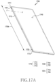
- FIG. 17A is a perspective view of an electronic device according to various embodiments.
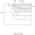
- FIG. 17B illustrates a cross section view taken along axis F-F' in the electronic device according to the embodiment of FIG. 17A .
- an electronic device 1700 may include a cover glass 1740, a display 1742, and a housing 1701 that define at least a portion of a first surface (or a "front surface").
- the electronic device 1700 according to an embodiment may be referred to as a tablet device.
- a second surface (or a "side surface") that is substantially perpendicular to the front surface of the electronic device 1700 may be substantially defined by the housing 1701.
- the housing 1701 may include, for example, conductive portions 1710 formed of a conductive material (e.g., aluminum, stainless steel (STS), or magnesium) and/or non-conductive portions 1720 formed of a non-conductive material (e.g., a polymer).
- the housing 1701 may include conductive portions 1710 and/or non-conductive portions 1720 that split the conductive portions 1710.
- the second edge 1720b of the housing 1701 may include a first conductive portion 1711, a first non-conductive portion 1721, a second conductive portion 1712, a second non-conductive portion 1722, and/or a third conductive portion 1713.
- a conductive portion may be replaceably understood as a conductive unit or a conductive region
- a non-conductive portion may be replaceably understood as a non-conductive unit or a split portion.
- the first conductive portion 1711, the second conductive portion 1712, or the third conductive portion 1713 may include a metallic material.
- the first conductive portion 1711, the second conductive portion 1712, and the third conductive portion 1713 may correspond to at least a portion of a metal housing.
- the first non-conductive portion 1721 or the second non-conductive portion 1722 may be formed of a dielectric material having a predetermined dielectric constant.
- the first non-conductive portion 1721 and the second non-conductive portion 1722 may be filled with a dielectric material.
- the wireless communication circuit (not illustrated) disposed within the housing 1701 may transmit/receive power by using at least one of the first conductive portion 1711, the second conductive portion 1712, or the third conductive portion 1713.
- a wireless communication circuit disposed on a printed circuit board within the housing 1701 may transmit and/or receive a radio signal by feeding power to at least one of the first conductive portion 1711, the second conductive portion 1712, or the third conductive portion.
- the conductive member 1750 (e.g., the conductive member 240 in FIG. 2A ) according to an embodiment may be disposed between the cover glass 1740 and the display circuit unit 1741.
- the conductive member 1750 according to an embodiment may be disposed between the conductive portions 1710 and the display circuit unit 1741.
- the conductive member 1750 may be disposed to be electrically separated from the first conductive portion 1711, the second conductive portion 1712, or the third conductive portion 1713.
- the conductive member 1750 may protect the display circuit unit 1741 from electrostatic discharge.
- the conductive member 1750 may provide a discharge path that transfers discharge occurring near a dielectric material (e.g., the dielectric material 230 in FIG. 2A ) to the conductive portions 1710 to prevent or suppress performance degradation of the display circuit unit 1741.
- a dielectric material e.g., the dielectric material 230 in FIG. 2A
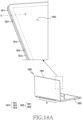
- FIG. 18A illustrates an electronic device according to still another embodiment.
- FIG. 18B illustrates a cross section view taken along axis G-G' in the electronic device according to the embodiment of FIG. 18A .
- an electronic device 1800 may include a first housing 1801, a hinge structure H, a second housing coupled to the first housing 1801 via the hinge structure H to be rotatable relative to the first housing 1801, and a display 1840.
- the first housing 1801 may be coupled to the second housing 1802 to rotate by a predetermined angle A relative to the second housing 1802 about the hinge structure H.
- the first housing 1801 may include conductive portions 1810 and non-conductive portions 1820 that define a side surface of the electronic device 1800.
- the conductive portions 1810 may be disposed to be electrically separated from each other by the non-conductive portions 1820.
- the first housing 1801 may include a first conductive portion 1811, a first non-conductive portion 1821, a second conductive portion 1812, a second non-conductive portion 1822, and/or a third conductive portions 1813.
- a conductive portion may be replaceably understood as a conductive unit or a conductive region
- a non-conductive portion may be replaceably understood as a non-conductive unit or a split portion.
- a wireless communication circuit (not illustrated) disposed within a housing 1801 or 1802 may transmit/receive a radio signal by using at least one of the conductive portions 1810 by feeding power to at least a portion of the housing 1801 or 1802.
- the wireless communication circuit disposed on a printed circuit board within the housing 1801 or 1802 may transmit and/or receive a radio signal by feeding power to at least one of the conductive portions 1810.
- a conductive member 1850 (e.g., the conductive member 240 in FIG. 2A ) according to an embodiment may be disposed between a dielectric material 1830 (e.g., the dielectric material 230 in FIG. 2A ) and a display circuit unit 1841.
- the conductive member 1850 may be disposed between the dielectric material 1830 and the display circuit unit 1841 to be adjacent to a dielectric material 1830.
- the dielectric material 1830 may be referred to as a decoration that protects the display circuit unit 1841 or the display (e.g., the display 1742 in FIG. 7 ).
- the electronic device 1800 may include a glass decoration 1831.
- the glass decoration 1831 may be provided to protect the display.
- the glass decoration 1831 may be disposed adjacent to the conductive member 1850.
- the glass decoration 1831 according to an embodiment may be formed of a dielectric material having a predetermined dielectric constant.
- the conductive member 1850 may protect the display circuit unit 1841 from electrostatic discharge.
- the conductive member 1850 may provide a discharge path that transfers discharge occurring near a dielectric material (e.g., the dielectric material 230 in FIG. 2A ) to the conductive portions 1810 to prevent or suppress performance degradation of the display circuit unit 1841.
- a dielectric material e.g., the dielectric material 230 in FIG. 2A
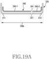
- FIG. 19A illustrates a housing including a single non-conductive portion and a conductive member according to an embodiment.
- FIG. 19B illustrates a housing including a single non-conductive portion and a side non-conductive portion and a conductive member according to an embodiment.
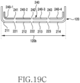
- FIG. 19C illustrates a housing including a plurality of non-conductive portions and a conductive member according to an embodiment.
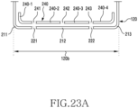
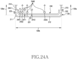
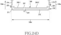
- some of the edges of the second housing 120 may include a plurality of conductive portions 211, 212, 213, and 214 and at least one non-conductive portion 221, 222, or 223.
- the conductive member 240 may include a plurality of conductive member portions 240-1, 240-2, 240-3, and 240-4 and at least one split portion 241, 242, or 243.
- a fourth edge 120b of the second housing 120 may include a first conductive portion 211, a first non-conductive portion 221, and a second conductive portion 212.
- the conductive member 240 may include a first conductive member portion 240-1, a first split portion 241, and a second conductive member portion 240-2.
- the first non-conductive portion 221 of the second housing 120 and the first split portion 241 of the conductive member 240 may be disposed at positions corresponding to each other.
- the first non-conductive portion 221 of the second housing 120 and the first split portion 241 of the conductive member 240 may be disposed to at least partially overlap each other.
- a fourth edge 120b of the second housing 120 may include a first conductive portion 211, a first non-conductive portion 221, and a second conductive portion 212.
- a third edge 120a of the second housing 120 may include a portion of the second conductive portion 212, a fifth non-conductive portion 225, and a fifth conductive portion 215.
- a fifth edge 120e perpendicular to the fourth edge 120b and parallel to the third edge 120a may include a portion of the first conductive portion 211, a fourth non-conductive portion 224, and a fourth conductive portion 214.
- the conductive member 240 may include a first conductive member portion 240-1, a first split portion 241, and a second conductive member portion 240-2.
- the first non-conductive portion 221 of the second housing 120 and the first split portion 241 of the conductive member 240 may be disposed at positions corresponding to each other.
- the first non-conductive portion 221 of the second housing 120 and the first split portion 241 of the conductive member 240 may be disposed to at least partially overlap each other.
- one end of the first conductive member portion 240-1 may be disposed to correspond to the fourth non-conductive portion 224.
- one end of the second conductive member portion 240-2 may be disposed to correspond to the fifth non-conductive portion 225.
- the fourth edge 120b of the second housing 120 may include a first conductive portion 211, a first non-conductive portion 221, a second conductive portion 212, a second non-conductive portion 222, a third conductive portion 213, a third non-conductive portion 223, and a fourth conductive portion 214.
- the conductive member 240 may include a first conductive member portion 240-1, a first split portion 241, a second conductive member portion 240-2, a second split portion 242, a third conductive member portion 240-3, a third split portion 243, and a fourth conductive member portion 240-4.
- the non-conductive portions 221, 222, and 223 of the second housing 120 may be provided to respectively correspond to the split portions 241, 242, and 243 of the conductive member 240.
- the first non-conductive portion 221 of the second housing 120 and the first split portion 241 of the conductive member 240 may be disposed at positions corresponding to each other.
- the first non-conductive portion 221 of the second housing 120 and the first split portion 241 of the conductive member 240 may be disposed to at least partially overlap each other.
- the second non-conductive portion 222 of the second housing 120 and the second split portion 242 of the conductive member 240 may be disposed to at least partially overlap each other.
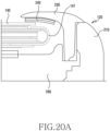
- FIG. 20A illustrates a conductive member disposed adjacent to a dielectric material according to an embodiment.
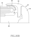
- FIG. 20B illustrates a conductive member disposed adjacent to a display according to an embodiment.
- FIG. 20C illustrates a conductive member disposed adjacent to a housing according to an embodiment.
- an electronic device (e.g., the electronic device 100 in FIG. 1 ) may include a second housing 120 including conductive portions 210, a display 140, a dielectric material 230 disposed to surround at least a portion of the perimeter of the display 140, a dielectric material 230, and a conductive member 240 disposed between the dielectric material 230 and the display 140.
- the second housing 120 may include an injection-molded part 290 having a predetermined dielectric constant.
- the injection-molded part 290 may be formed of a non-conductive material.
- the dielectric material 230 may be disposed between an edge (e.g., the fourth edge 120b in FIG. 2B ) of the second housing 120 and the display 140.
- the conductive member 240 may be disposed between the dielectric material 230 and the display 140 to be adjacent to the dielectric material 230.
- the conductive member 240 may be disposed to be attached to one surface of the dielectric material 230 that faces the display 140.
- the conductive member 240 may be disposed between the dielectric material 230 and the display 140 to be adjacent to the display 140.
- the conductive member 240 may be disposed to be attached to one surface of the display 140 that faces the dielectric material 230.
- the conductive member 240 may be attached to one surface of the display 140 that faces the dielectric material 230 via an adhesive member 247 (or a support member).
- the conductive member 240 may be disposed adjacent to the second housing 120. According to an embodiment, the conductive member 240 may be disposed adjacent to an edge of the second housing 120. For example, the conductive member 240 may be disposed to be attached to one surface that is adjacent to an edge (e.g., the fourth edge 120b in FIG. 2B ) of the second housing 120 and faces the inside of the electronic device.
- an edge e.g., the fourth edge 120b in FIG. 2B
- the conductive member 240 may be attached to the one surface that is adjacent to an edge of the second housing 120 and faces the inside of the electronic device via the adhesive member 247 (or a support member).
- FIG. 21A illustrates a housing including a plurality of non-conductive portions and a conductive member according to an embodiment.
- FIG. 21B illustrates a housing including a plurality of non-conductive portions and a conductive member having a single split portion according to an embodiment.
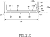
- FIG. 21C illustrates a housing including a plurality of non-conductive portions and a side non-conductive portion, and a conductive member including a split portion corresponding to at least one non-conductive portion according to an embodiment.
- FIG. 21D illustrates a housing including a plurality of non-conductive portions and a side non-conductive portion, and a conductive member including a split portion corresponding to at least one non-conductive portion according to another embodiment.
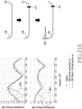
- FIG. 21E illustrating graphs each showing antenna radiation efficiency according to a change in length of a conductive member according to an embodiment.
- some of the edges of a second housing 120 may include a plurality of conductive portions 211, 212, 213, and 214 and at least one non-conductive portion 221, 222, or 223.
- the conductive member 240 may include a plurality of conductive member portions 240-1, 240-2, and 240-3 and at least one split portion 241 or 242.
- a fourth edge 120b of the second housing 120 may include at least a portion of a first conductive portion 211, a first non-conductive portion 221, a second conductive portion 212, a second non-conductive portion 222, and at least a portion of a third conductive portion 213.
- the conductive member 240 may include a first conductive member portion 240-1 corresponding to the second conductive portion 212 of the second housing 120.
- the second conductive portion 212 of the second housing 120 and the first conductive member part 240-1 of the conductive member 240 may be disposed at positions corresponding to each other.
- a fourth edge 120b of the second housing 120 may include at least a portion of the first conductive portion 211, the first non-conductive portion 221, the second conductive portion 212, the second non-conductive portion 222, and at least a portion of the third conductive portion 213.
- the conductive member 240 may include a first conductive member portion 240-1, a first split portion 241, and a second conductive member portion 240-2.
- the second non-conductive portion 222 of the second housing 120 and the first split portion 241 of the conductive member 240 may be disposed at positions corresponding to each other.
- the first non-conductive portion 221 of the second housing 120 and the first split portion 241 of the conductive member 240 may be disposed to at least partially overlap each other.
- one end of the first conductive member portion 240-1 may be disposed to correspond to the second non-conductive portion 222.
- the first conductive member portion 240-1 may correspond to or overlap at least a portion of the first conductive portion 211, the first non-conductive portion 221, or the second conductive portion 212.
- the second conductive member portion 240-2 may correspond to or overlap the third conductive portion 213.
- the fourth edge 120b of the second housing 120 may include at least a portion of the first conductive portion 211, the first non-conductive portion 221, the second conductive portion 212, the second non-conductive portion 222, and at least a portion of the third conductive portion 213.
- a third edge 120a of the second housing 120 according to an embodiment may include another portion of the second conductive portion 213, a third non-conductive portion 223, and at least a portion of a fourth conductive portion 214.
- the conductive member 240 may include a first conductive member portion 240-1, a first split portion 241, a second conductive member portion 240-2, a second split portion 242, and a third conductive member portion 240-3.
- the non-conductive portions 221, 222, and 223 of the second housing 120 may be provided to respectively correspond to the split portions 241 and 242 of the conductive member 240.
- the second non-conductive portion 222 of the second housing 120 and the first split portion 241 of the conductive member 240 may be disposed at positions corresponding to each other.
- the third non-conductive portion 223 of the second housing 120 and the second split portion 242 of the conductive member 240 may be disposed to at least partially overlap each other.
- the first conductive member portion 240-1 may correspond to or overlap at least a portion of the first conductive portion 211, the first non-conductive portion 221, or the second conductive portion 212.
- the second conductive member portion 240-2 may correspond to or overlap the third conductive portion 213.
- the third conductive member portion 240-3 may correspond to or overlap the fourth conductive portion 214.
- a fourth edge 120b of the second housing 120 may include at least a portion of the first conductive portion 211, the first non-conductive portion 221, the second conductive portion 212, the second non-conductive portion 222, and at least a portion of the third conductive portion 213.
- a third edge 120a of the second housing 120 may include a portion of the third conductive portion 213, a third non-conductive portion 223, and a fourth conductive portion 214.
- a fifth edge 120e of the second housing 120 perpendicular to the fourth edge 120b and substantially parallel to the third edge 120a may include a portion of the first conductive portion 211, a fourth non-conductive portion 224, and a fifth conductive portion 215.
- the conductive member 240 may include a first conductive member portion 240-1, a first split portion 241, and a second conductive member portion 240-2.
- the non-conductive portions 221, 222, and 223 of the second housing 120 may be provided to respectively correspond to the split portions 241 and 242 of the conductive member 240.
- the second non-conductive portion 222 of the second housing 120 and the first split portion 241 of the conductive member 240 may be disposed at positions corresponding to each other.
- the third non-conductive portion 223 of the second housing 120 and the second split portion 242 of the conductive member 240 may be disposed to at least partially overlap each other.
- one end of the first conductive member portion 240-1 may be disposed to correspond to the fourth non-conductive portion 224.
- one end of the second conductive member portion 240-2 may be disposed to correspond to the third non-conductive portion 223.
- the first conductive member portion 240-1 may correspond to or overlap at least a portion of the first conductive portion 211, the first non-conductive portion 221, or the second conductive portion 212.
- the second conductive member portion 240-2 may correspond to or overlap the third conductive portion 213.
- the conductive member 240 since the conductive member 240 according to an embodiment includes an extension portion 249 extending from one end thereof, antenna radiation performance may be improved.
- parasitic resonance 2201 may occur compared to the case in which the conductive member 240 does not include the first split portion 241.
- the antenna radiation performance may be deteriorated since parasitic resonance 2201 occurs in a predetermined frequency band. For example, when the conductive member 240 includes the first split portion 241, parasitic resonance 2201 occurs in the frequency band of about 1600 MHz to about 1700 MHz, and thus antenna radiation performance may be deteriorated.
- parasitic resonance 2201 when the conductive member 240 includes the first split portion 241 and the extension portion 249 extending from one end of the conductive member 240, parasitic resonance 2201, which occurs when the conductive member 240 only includes the first split portion 241 without including the extension portion 249, may not occur.
- the conductive member 240 since the conductive member 240 includes the first split portion 241 and the extension portion 249, it is possible to prevent/reduce the occurrence of parasitic resonance 2201 and to prevent/reduce deterioration of antenna performance.
- FIG. 22 illustrates a housing including three or more non-conductive portions and a conductive member having a split portion corresponding to at least one non-conductive portion according to an embodiment.
- the fourth edge 120b of the second housing 120 may include at least a portion of a first conductive portion 211, a first non-conductive portion 221, a second conductive portion 212, a second non-conductive portion 222, a third conductive portion 213, a third non-conductive portion 223, and a portion of a fourth conductive portion 214.
- the third edge 120a of the second housing 120 may include a portion of the fourth conductive portion 214.
- the conductive member 240 may include a first conductive member portion 240-1, a first split portion 241, a second conductive member portion 240-2, a second split portion 242, or a third conductive member portion 240-3.
- the non-conductive portions 221, 222, and 223 of the second housing 120 may be provided to respectively correspond to the split portions 241 and 242 of the conductive member 240.
- the first non-conductive portion 221 of the second housing 120 and the first split portion 241 of the conductive member 240 may be disposed at positions corresponding to each other.
- the third non-conductive portion 223 of the second housing 120 and the second split portion 242 of the conductive member 240 may be disposed to at least partially overlap each other.
- FIG. 23A illustrates a housing including a conductive member including a plurality of split portions and non-conductive portions corresponding to at least some of the plurality of split portions according to another embodiment.
- FIG. 23B illustrates a housing including a plurality of non-conductive portions and a conductive member including split portions corresponding to at least some of the plurality of non-conductive portions according to another embodiment.
- FIG. 23C illustrates a conductive member in which protrusions are provided according to another embodiment.
- a fourth edge 120b of the second housing 120 may include at least a portion of a first conductive portion 211, a first non-conductive portion 221, a second conductive portion 212, a second non-conductive portion 222, and/or a third conductive portion 213.
- the conductive member 240 may include a plurality of conductive member portions 240-1, 240-2, 240-3, and 240-4 and at least one split portion 241, 242, or 243.
- a fourth edge 120b of the second housing 120 may include at least a portion of a first conductive portion 211, a first non-conductive portion 221, a second conductive portion 212, a second non-conductive portion 222, and at least a portion of a third conductive portion 213.
- the conductive member 240 may include a first conductive member portion 240-1, a first split portion 241, a second conductive member portion 240-2, a second split portion 242, a third conductive member portion 240-3, a third split portion 243, and a fourth conductive member portion 240-4.
- the split portions 241, 242, and 243 of the conductive member 240 may be provided to respectively correspond to the non-conductive portions 221 and 222 of the housing 120.
- the first non-conductive portion 221 of the second housing 120 and the first split portion 241 of the conductive member 240 may be disposed at positions corresponding to each other.
- the first non-conductive portion 221 of the second housing 120 and the first split portion 241 of the conductive member 240 may be disposed to at least partially overlap each other.
- the second non-conductive portion 222 of the second housing 120 and the third split portion 243 of the conductive member 240 may be disposed at positions corresponding to each other.
- the second non-conductive portion 222 of the second housing 120 and the third split portion 243 of the conductive member 240 may be disposed to at least partially overlap each other.
- the first conductive member portion 240-1 of the conductive member 240 may be provided to overlap at least a portion of the first conductive portion 211 of the second housing 120.
- the second conductive member portion 240-2 and the third conductive member portion 240-3 of the conductive member 240 may be provided to overlap at least a portion of the second conductive portion 212 of the second housing 120.
- the fourth conductive member portion 240-4 of the conductive member 240 may be provided to overlap at least a portion of the third conductive portion 213 of the second housing 120.
- the second split portion 242 of the conductive member 240 may be provided to correspond to at least a portion of the second conductive portion 212 of the second housing 120.
- the fourth edge 120b of the second housing 120 may include at least a portion of the first conductive portion 211, the first non-conductive portion 221, the second conductive portion 212, the second non-conductive portion 222, the third conductive portion 213, the third non-conductive portion 223, and the fourth conductive portion 214.
- the conductive member 240 may include a first conductive member portion 240-1, a first split portion 241, a second conductive member portion 240-2, a second split portion 242, and a third conductive member portion 240-3.
- the non-conductive portions 221, 222, and 223 of the second housing 120 may be provided to respectively correspond to the split portions 241 and 242 of the conductive member 240.
- the first non-conductive portion 221 of the second housing 120 and the first split portion 241 of the conductive member 240 may be disposed at positions corresponding to each other.
- the first non-conductive portion 221 of the second housing 120 and the first split portion 241 of the conductive member 240 may be disposed to at least partially overlap each other.
- the third non-conductive portion 223 of the second housing 120 and the second split portion 242 of the conductive member 240 may be disposed to at least partially overlap each other.
- the first conductive member portion 240-1 of the conductive member 240 may be provided to overlap at least a portion of the first conductive portion 211 of the second housing 120.
- at least a portion of the second conductive member portion 240-2 of the conductive member 240 may be provided to overlap at least a portion of the second conductive portion 212 and the third conductive portion 213 of the second housing 120.
- the third conductive member portion 240-3 of the conductive member 240 may be provided to overlap at least a portion of the fourth conductive portion 214 of the second housing 120.
- the second non-conductive portion 222 of the second housing 120 may be provided to correspond to at least a portion of the second conductive member portion 240-2 of the conductive member 240.
- the second conductive member portion 240-2 of the conductive member 240 may include a first protrusion 2210, and the third conductive member portion 240-3 may include a second protrusion 2220.
- the first protrusion 2210 may provide a discharge path such that discharge occurring at a position adjacent to the second conductive member portion 240-2 flows to the second conductive portion 212.
- the first protrusion 2210 may prevent/reduce electrostatic discharge more effectively.
- the second protrusion 2220 may provide a discharge path such that discharge occurring at a position adjacent to the third conductive member portion 240-3 flows to the third conductive portion 213.
- the second protrusion 2220 may prevent/reduce electrostatic discharge more effectively.
- FIG. 24A illustrates a housing including a non-conductive portion and a conductive member according to an embodiment.
- FIG. 24B illustrates a housing including a non-conductive portion and a conductive member including a split portion corresponding to at least a portion of the non-conductive portion according to an embodiment.
- FIG. 24C illustrates a housing including a non-conductive portion and a conductive member according to an embodiment.
- FIG. 24D illustrates a housing including a non-conductive portion and a conductive member including a split portion corresponding to at least a portion of the non-conductive portion according to an embodiment.
- FIG. 24E illustrates graphs each showing antenna radiation performance according to alignment of a non-conductive portion of a housing and a split portion of a conductive member according to an embodiment.
- the fourth edge 120b of the second housing 120 may include at least a portion of a first conductive portion 211, a first non-conductive portion 221, and at least a portion of a second conductive portion 212.
- the third edge 120a of the second housing 120 may include another portion of the second conductive portion 212, a second non-conductive portion 222, and a third conductive portion 213.
- the fifth edge 120e of the second housing 120 perpendicular to the fourth edge 120b and parallel to the third edge 120a may include another portion of the first conductive portion 211, a third non-conductive portion 223, and a fourth conductive portion 214.
- the electronic device may include a conductive member 240 disposed adjacent to the second housing 120.
- a wireless communication circuit may transmit/receive a signal in a predetermined frequency band by feeding power to the first conductive portion 211 and the second conductive portion 212.
- the wireless communication circuit may use the first conductive portion 211 and the second conductive portion 212 as antenna radiators.
- the wireless communication circuit may transmit/receive a signal in a predetermined frequency band by feeding power to a first point 2411 of the first conductive portion 211. According to an embodiment, the wireless communication circuit may transmit/receive a signal in a predetermined frequency band by feeding power to a second point 2412 of the first conductive portion 212.
- the first conductive portion 211 and the second conductive portion 212 of the second housing 120 may be electrically connected to a ground.
- the first conductive portion 211 may be electrically connected to a ground via a first ground point 2421 and/or a second ground point 2422.
- the second conductive portion 212 may be electrically connected to a ground via a third ground point 2423.
- the first conductive portion 211 and the second conductive portion 212 of the second housing 120 may be electrically connected to a ground via at least one electronic element 2440.
- At least one electronic element 2440 may be referred to as one of a matching circuit, a switch, or a tuner.
- the at least one electronic element 2440 may be referred to as a matching circuit, and an antenna radiation characteristic via the first conductive portion 211 and the second conductive portion 212 may be controlled through the matching circuit.
- the electronic element 2440 may be referred to as a plurality of matching circuits having different structures.
- FIG. 24A The feeding structure and the ground connection structure of FIG. 24A may be equally applied to FIGS. 24B , 24C , and 24D .
- an edge of the second housing 120 may include a first conductive portion 211, a first non-conductive portion 221, and a second conductive portion 212.
- the third edge 120a of the second housing 120 may include a portion of the second conductive portion 212, a second non-conductive portion 222, and a third conductive portion 213.
- the fifth edge 120e of the second housing 120 perpendicular to the fourth edge 120b and parallel to the third edge 120a may include another portion of the first conductive portion 211, a third non-conductive portion 223, and a fourth conductive portion 214.
- the conductive member 240 disposed adjacent to the second housing 120 may include a first conductive member portion 240-1, a first split portion 241, and a second conductive member portion 240-2.
- the first non-conductive portion 221 of the second housing 120 and the first split portion 241 of the conductive member 240 may be disposed at positions corresponding to each other.
- the first non-conductive portion 221 of the second housing 120 and the first split portion 241 of the conductive member 240 may be disposed to at least partially overlap each other.
- one end of the conductive member 240 may be provided to correspond to the third non-conductive portion 223.
- the other end of the conductive member 240 according to an embodiment may be provided to correspond to the second non-conductive portion 222.
- the conductive member 240 may include a first conductive member portion 240-1, a first split portion 241, and a second conductive member portion 240-2.
- one end of the first conductive member portion 240-1 of the conductive member 240 may be provided to correspond to the third non-conductive portion 223.
- one end of the second conductive member portion 240-2 of the conductive member 240 may be provided to correspond to the second non-conductive portion 222.
- the first split portion 241 of the conductive member 240 may be provided to correspond to the first non-conductive portion 221 of the second housing 120.
- antenna radiation performance may vary depending on the alignment of the split portion of the conductive member 240 and the non-conductive portions 221, 222, and 223 of the second housing 120.
- the antenna radiation efficiency may be increased as a corresponding area between the split portion and the non-conductive portion is spaced apart from a point (e.g., the first point 2411) fed with power from the wireless communication circuit.
- the antenna radiation efficiency may be improved when the conductive member 240 is provided such that one end corresponds to the third non-conductive portion 223 and the other end corresponds to the second non-conductive portion 222 (e.g., FIG. 24C ).
- the antenna radiation efficient may be high when the conductive member 240 is provided such that one end corresponds to the third non-conductive portion 223 and the other end corresponds to the second non-conductive portion 222 while the first split portion 241 is provided to correspond to the first non-conductive portion 221 (e.g., FIG. 24D ).
- the antenna radiation efficiency may be improved when the conductive member 240 is provided such that one end corresponds to the third non-conductive portion 223 and the other end corresponds to the second non-conductive portion 222 (e.g., FIG. 24C ).
- the antenna radiation efficiency may be improved when the conductive member 240 is provided such that one end corresponds to the third non-conductive portion 223 and the other end corresponds to the second non-conductive portion 222 while the first split portion 241 is provided to correspond to the first non-conductive portion 221 (e.g., FIG. 24C ).
- the bandwidth of a first frequency band may decrease, and the antenna radiation performance in a second frequency band (e.g., a mid-band (MB)) may be deteriorated.
- a first frequency band e.g., a low band (LB)
- LB low band
- MB mid-band
- FIG. 25A illustrates an electronic device including a conductive member provided to be adjacent to a conductive portion used as an antenna radiator when the electronic device is in an unfolded state, according to an embodiment.
- FIG. 25B illustrates an electronic device including a conductive member provided to be adjacent to a conductive portion used as an antenna radiator when the electronic device is in a folded state, according to an embodiment.
- FIG. 25C illustrates an electronic device including a conductive member formed to be adjacent to a conductive portion used as an antenna radiator when the electronic device is in an unfolded state and a folded state, according to an embodiment.
- the conductive member 2540 may be disposed adjacent to the display circuit unit 2541 and a region that operates by being fed with power from a wireless communication circuit of the housing 2510 or 2520 depending on the folded or unfolded state of the electronic device 2500.
- the electronic device 2500 of FIGS. 25A to 25B may be referred to as the electronic device 1500 of FIG. 15 .
- a wireless communication circuit (not illustrated) may transmit/receive a signal in a predetermined frequency band by feeding power to the first conductive portion 2511 and the second conductive portion 2512 of the first housing 2510.
- the wireless communication circuit may use the first conductive portion 2511 and the second conductive portion 2512 as antenna radiators.
- the display circuit unit 2541 may be disposed adjacent to the first conductive portion 2511 and the second conductive portion 2512.
- the conductive member 2540 may be disposed between the display circuit unit 2541 and the first conductive portion 2511 and/or the second conductive portion 2512.
- the conductive member 2540 may be disposed between the display circuit unit 2541 and the first conductive portion 2511 and/or the second conductive portion 2512 to prevent/reduce electrostatic discharge to the display circuit unit 1541.
- the conductive member 2540 may cause static electricity generated from a dielectric material (e.g., the dielectric material 230 in FIG. 2A ) to flow to a portion of the conductive member 2540, the first conductive portion 2511, or the second conductive portion 2512, thereby preventing/reducing the static electricity from being transferred to the display circuit unit 2541.
- a wireless communication circuit (not illustrated) may transmit/receive a signal in a predetermined frequency band by feeding power to the first conductive portion 2511 and the second conductive portion 2512 of the first housing 2510.
- the wireless communication circuit may use the first conductive portion 2511 and the second conductive portion 2512 as antenna radiators.
- the display circuit unit 2541 may be disposed adjacent to the fifth conductive portion 2515 and the sixth conductive portion 2516 of the second housing 2520. According to an embodiment, when the electronic device 2500 is in a folded state, the display circuit unit 2541 may be disposed adjacent to the first conductive portion 2511 and the second conductive portion 2512 used as antenna radiators.
- the conductive member 2540 may be disposed between the display circuit unit 2541 and the fifth conductive portion 2515 and/or the sixth conductive portion 2516.
- the conductive member 2540 may be disposed adjacent to the first conductive portion 2511 and the second conductive portion 2512 when the electronic device 2500 is in a folded state. According to an embodiment, when the electronic device 2500 is in a folded state, the conductive member 2540 may be disposed adjacent to the first conductive portion 2511 and the second conductive portion 2512, thereby preventing/reducing electrostatic discharge to the display circuit unit 1541.
- the conductive member 2540 may cause static electricity generated from a dielectric material (e.g., the dielectric material 230 in FIG. 2A ) to flow to a portion of the conductive member 2540, the fifth conductive portion 2515, or the sixth conductive portion 2516, thereby preventing/reducing the static electricity from being transferred to the display circuit unit 2541.
- a dielectric material e.g., the dielectric material 230 in FIG. 2A
- a wireless communication circuit (not illustrated) may transmit/receive a signal in a predetermined frequency band by feeding power to the first conductive portion 2511 and the second conductive portion 2512 of the first housing 2510, and the fifth conductive portion 2515 and the sixth conductive portion 2516 of the second housing 2520.
- the wireless communication circuit may use the first conductive portion 2511 and the second conductive portion 2512 of the first housing 2510, and the fifth conductive portion 2515 and the sixth conductive portion 2516 of the second housing 2520 as antenna radiators by feeding power thereto.
- the display circuit unit 2541 may be disposed adjacent to the fifth conductive portion 2515 and the sixth conductive portion 2516 of the second housing 2520. According to an embodiment, when the electronic device 2500 is in a folded state, the display circuit unit 2541 may be disposed adjacent to the first conductive portion 2511 and the second conductive portion 2512 used as antenna radiators.
- the conductive member 2540 may be disposed between the display circuit unit 2541 and the fifth conductive portion 2515 and/or the sixth conductive portion 2516.
- the conductive member 2540 may be disposed between the display circuit unit 2541 and the fifth conductive portion 2515 and/or the sixth conductive portion 2516 to prevent/reduce electrostatic discharge to the display circuit unit 1541.
- the conductive member 2540 may cause static electricity generated from a dielectric material (e.g., the dielectric material 230 in FIG. 2A ) to flow to a portion of the conductive member 2540, the fifth conductive portion 2515, and/or the sixth conductive portion 2516, thereby preventing/reducing the static electricity from being transferred to the display circuit unit 2541.
- a dielectric material e.g., the dielectric material 230 in FIG. 2A
- the conductive member 2540 may be disposed adjacent to the first conductive portion 2511 and the second conductive portion 2512 when the electronic device is in a folded state.
- the conductive member 2540 when the electronic device is in a folded state, the conductive member 2540 may be disposed adjacent to the first conductive portion 2511 and the second conductive portion 2512, thereby preventing/reducing electrostatic discharge to the display circuit unit 1541.
- the conductive member 2540 may cause static electricity generated from a dielectric material (e.g., the dielectric material 230 in FIG. 2A ) to flow to a portion of the conductive member 2540, the fifth conductive portion 2515, or the sixth conductive portion 2516, thereby preventing the static electricity from being transferred to the display circuit unit 2541.
- a dielectric material e.g., the dielectric material 230 in FIG. 2A
- An electronic device may include: a first housing including a first edge oriented in a first direction and a second edge oriented in a second direction perpendicular to the first direction; a second housing connected to the first housing via a connecting member to be rotatable relative to the first housing, wherein the second housing 120 includes a third edge corresponding to the first edge and a fourth edge corresponding to the second edge when the first housing and the second housing face each other; a flexible display defining a front surface of the electronic device and is disposed over the first housing and the second housing; a dielectric material at least partially disposed between the flexible display and the fourth edge of the second housing while at least partially surrounding a perimeter of the flexible display; a conductive member located between the dielectric material and the flexible display; and a wireless communication circuit disposed within the first housing or the second housing, wherein the fourth edge may include a first conductive portion, a first non-conductive portion, a second conductive portion, a second non-conductive portion, and a third conductive portion, the fourth edge may include
- the wireless communication circuit may be disposed on a printed circuit board, and the conductive member may be disposed between the dielectric material and the printed circuit board.
- the conductive member may include a first conductive member portion, a second conductive member portion, or a third conductive member portion.
- the first split portion or the second split portion may be comprise a dielectric material having a predetermined dielectric constant.
- the first split portion and the second split portion may have a length of at least 0.5 mm.
- the flexible display may further include a display circuit unit disposed under the flexible display.
- the conductive member may be a tape including a flexible conductive adhesive layer.
- the second conductive member portion may include at least one protrusion.
- the at least one protrusion may include a plurality of first protrusions or a plurality of second protrusions.
- the at least one protrusion may include a first protrusion, and the first protrusion may extend from one end of the first conductive member portion to at least partially face the first conductive portion.
- the at least one protrusion may include a second protrusion, and the second protrusion may extend from one end of the first conductive member portion toward the first conductive portion to be adjacent to the first conductive portion.
- the first conductive member portion or the third conductive portion may include at least one protrusion.
- the at least one protrusion may include a first protrusion, and the first protrusion may extend from one end of the first conductive member portion to at least partially face the first conductive portion.
- the at least one protrusion may include a second protrusion, and the second protrusion may extend from one end of the first conductive member portion toward the first conductive portion to be adjacent to the first conductive portion.
- the second conductive portion may include a first feeding point, and the first protrusion included in the second conductive member portion may be provided at one point of the second conductive member portion to be spaced apart from the first feeding point.
- An electronic device may include: a housing including a first edge oriented in a first direction and a second edge oriented in a second direction perpendicular to the first direction; a display defining a front surface of the electronic device; a dielectric material at least partially disposed between the display and the second edge of the housing and at least partially surrounding a perimeter of the display; a conductive member comprising a conductive material located between the dielectric material and the display; and a wireless communication circuit disposed within the housing, wherein the second edge may include a first conductive portion, a second conductive portion, and a first non-conductive portion disposed between the first conductive portion and the second conductive portion, the conductive member may be provided with a first split portion to correspond to the first non-conductive portion of the second edge of the housing, and the wireless communication circuit may be configured to transmit/receive a radio signal by using at least one of the first conductive portion and the second conductive portion of the housing.
- the conductive member may include a first conductive member portion or a second conductive member portion.
- the first split portion may comprise with a dielectric material having a predetermined dielectric constant.
- the electronic device may further include a display circuit unit disposed under the display.
- the first conductive member portion or the second conductive member portion may include at least one protrusion.
- the electronic device may be one of various types of electronic devices.
- the electronic devices may include, for example, a portable communication device (e.g., a smartphone), a computer device, a portable multimedia device, a portable medical device, a camera, a wearable device, or a home appliance. According to an embodiment of the disclosure, the electronic devices are not limited to those described above.
- each of such phrases as “A or B,” “at least one of A and B,” “at least one of A or B,” “A, B, or C,” “at least one of A, B, and C,” and “at least one of A, B, or C,” may include any one of, or all possible combinations of the items enumerated together in a corresponding one of the phrases.
- such terms as “1st” and “2nd,” or “first” and “second” may be used to simply distinguish a corresponding component from another, and does not limit the components in other aspect (e.g., importance or order).
- an element e.g., a first element
- the element may be coupled with the other element directly (e.g., wiredly), wirelessly, or via a third element.
- module may include a unit implemented in hardware, software, or firmware, and may interchangeably be used with other terms, for example, “logic,” “logic block,” “part,” or “circuitry”.
- a module may be a single integral component, or a minimum unit or part thereof, adapted to perform one or more functions.
- the module may be implemented in a form of an application-specific integrated circuit (ASIC).
- ASIC application-specific integrated circuit
- Various embodiments as set forth herein may be implemented as software (e.g., the program 1440) including one or more instructions that are stored in a storage medium (e.g., internal memory 1436 or external memory 1438) that is readable by a machine (e.g., the electronic device 1401).
- a processor e.g., the processor 1420
- the machine e.g., the electronic device 1401
- the one or more instructions may include a code generated by a complier or a code executable by an interpreter.
- the machine-readable storage medium may be provided in the form of a non-transitory storage medium.
- non-transitory simply means that the storage medium is a tangible device, and does not include a signal (e.g., an electromagnetic wave), but this term does not differentiate between where data is semi-permanently stored in the storage medium and where the data is temporarily stored in the storage medium.
- a method may be included and provided in a computer program product.
- the computer program product may be traded as a product between a seller and a buyer.
- the computer program product may be distributed in the form of a machine-readable storage medium (e.g., compact disc read only memory (CD-ROM)), or be distributed (e.g., downloaded or uploaded) online via an application store (e.g., PlayStoreTM), or between two user devices (e.g., smart phones) directly. If distributed online, at least part of the computer program product may be temporarily generated or at least temporarily stored in the machine-readable storage medium, such as memory of the manufacturer's server, a server of the application store, or a relay server.
- CD-ROM compact disc read only memory
- an application store e.g., PlayStoreTM
- two user devices e.g., smart phones
- each component e.g., a module or a program of the above-described components may include a single entity or multiple entities, and some of the multiple entities may be separately disposed in different components.
- one or more of the above-described components may be omitted, or one or more other components may be added.
- a plurality of components e.g., modules or programs
- the integrated component may still perform one or more functions of each of the plurality of components in the same or similar manner as they are performed by a corresponding one of the plurality of components before the integration.
- operations performed by the module, the program, or another component may be carried out sequentially, in parallel, repeatedly, or heuristically, or one or more of the operations may be executed in a different order or omitted, or one or more other operations may be added.
Landscapes
- Engineering & Computer Science (AREA)
- Theoretical Computer Science (AREA)
- Computer Networks & Wireless Communication (AREA)
- Physics & Mathematics (AREA)
- General Physics & Mathematics (AREA)
- Signal Processing (AREA)
- Human Computer Interaction (AREA)
- General Engineering & Computer Science (AREA)
- Support Of Aerials (AREA)
- Details Of Aerials (AREA)
- Transceivers (AREA)
- Shielding Devices Or Components To Electric Or Magnetic Fields (AREA)
Applications Claiming Priority (3)
| Application Number | Priority Date | Filing Date | Title |
|---|---|---|---|
| KR20210105677 | 2021-08-10 | ||
| KR1020210180895A KR20230023538A (ko) | 2021-08-10 | 2021-12-16 | 안테나를 포함하는 전자 장치 |
| PCT/KR2022/011478 WO2023018099A1 (fr) | 2021-08-10 | 2022-08-03 | Dispositif électronique comprenant une antenne |
Publications (2)
| Publication Number | Publication Date |
|---|---|
| EP4336651A1 true EP4336651A1 (fr) | 2024-03-13 |
| EP4336651A4 EP4336651A4 (fr) | 2024-11-06 |
Family
ID=85200807
Family Applications (1)
| Application Number | Title | Priority Date | Filing Date |
|---|---|---|---|
| EP22856098.3A Pending EP4336651A4 (fr) | 2021-08-10 | 2022-08-03 | Dispositif électronique comprenant une antenne |
Country Status (6)
| Country | Link |
|---|---|
| US (2) | US12456795B2 (fr) |
| EP (1) | EP4336651A4 (fr) |
| JP (1) | JP2024531169A (fr) |
| AU (1) | AU2022326997A1 (fr) |
| WO (1) | WO2023018099A1 (fr) |
| ZA (1) | ZA202401428B (fr) |
Families Citing this family (1)
| Publication number | Priority date | Publication date | Assignee | Title |
|---|---|---|---|---|
| WO2025037934A1 (fr) * | 2023-08-16 | 2025-02-20 | 삼성전자 주식회사 | Dispositif électronique comprenant une antenne segmentée |
Family Cites Families (22)
| Publication number | Priority date | Publication date | Assignee | Title |
|---|---|---|---|---|
| KR101521658B1 (ko) | 2008-12-09 | 2015-05-29 | 엘지디스플레이 주식회사 | 액정표시장치 |
| US8634178B2 (en) | 2010-08-27 | 2014-01-21 | Apple Inc. | ESD protection in a very small form factor consumer electronic product |
| US9007748B2 (en) * | 2011-08-31 | 2015-04-14 | Apple Inc. | Two-shot knuckles for coupling electrically isolated sections of an electronic device and methods for making the same |
| KR101897772B1 (ko) * | 2012-02-15 | 2018-09-12 | 엘지전자 주식회사 | 이동 단말기 |
| KR101978204B1 (ko) | 2012-04-24 | 2019-05-14 | 엘지전자 주식회사 | 이동 단말기 |
| US9704663B2 (en) | 2012-05-21 | 2017-07-11 | Apple Inc. | Accessory button controller assembly |
| KR101771733B1 (ko) | 2012-08-29 | 2017-08-25 | 삼성전기주식회사 | Esd 보호패턴이 내장된 공통 모드 필터 |
| KR102019122B1 (ko) | 2012-12-13 | 2019-09-06 | 엘지전자 주식회사 | 이동 단말기 |
| KR101608226B1 (ko) | 2014-11-20 | 2016-04-14 | 주식회사 아모텍 | 감전보호소자 및 이를 구비한 휴대용 전자장치 |
| ES2954487T3 (es) * | 2015-02-06 | 2023-11-22 | Samsung Electronics Co Ltd | Dispositivo electrónico que incluye pantalla con área doblada |
| KR102464155B1 (ko) * | 2015-11-13 | 2022-11-11 | 삼성전자주식회사 | 안테나 장치 및 그것을 포함하는 전자 장치 |
| US10431874B2 (en) * | 2016-02-19 | 2019-10-01 | Samsung Electronics Co., Ltd. | Antenna device and electronic device including the same |
| KR102296158B1 (ko) * | 2017-03-28 | 2021-08-31 | 삼성전자주식회사 | 다중 급전 안테나 및 그것을 포함하는 전자 장치 |
| KR102321393B1 (ko) * | 2017-05-12 | 2021-11-03 | 삼성전자주식회사 | 안테나를 포함하는 전자 장치 |
| KR102367486B1 (ko) | 2017-11-09 | 2022-02-25 | 엘지디스플레이 주식회사 | 디스플레이 장치 |
| CN108666739B (zh) * | 2018-05-02 | 2021-03-23 | Oppo广东移动通信有限公司 | 天线组件、壳体组件及电子设备 |
| KR102556813B1 (ko) | 2018-10-16 | 2023-07-18 | 삼성전자 주식회사 | 단일 절연성 부분을 이용한 안테나 및 그것을 포함하는 전자 장치 |
| US11095048B2 (en) * | 2018-12-13 | 2021-08-17 | Fitbit, Inc. | Multiple band antenna structures |
| KR102607569B1 (ko) | 2019-02-19 | 2023-11-30 | 삼성전자주식회사 | 안테나 및 이를 포함하는 전자 장치 |
| KR102786900B1 (ko) * | 2019-09-11 | 2025-03-26 | 삼성전자주식회사 | 안테나를 포함하는 폴더블 전자 장치 |
| CN210671188U (zh) * | 2019-10-30 | 2020-06-02 | 维沃移动通信有限公司 | 一种电子设备 |
| KR102718911B1 (ko) * | 2019-12-20 | 2024-10-23 | 삼성전자주식회사 | 안테나 및 이를 포함하는 전자 장치 |
-
2022
- 2022-08-03 AU AU2022326997A patent/AU2022326997A1/en active Pending
- 2022-08-03 JP JP2024508109A patent/JP2024531169A/ja active Pending
- 2022-08-03 EP EP22856098.3A patent/EP4336651A4/fr active Pending
- 2022-08-03 WO PCT/KR2022/011478 patent/WO2023018099A1/fr not_active Ceased
-
2023
- 2023-05-08 US US18/313,812 patent/US12456795B2/en active Active
-
2024
- 2024-02-16 ZA ZA2024/01428A patent/ZA202401428B/en unknown
-
2025
- 2025-10-27 US US19/369,522 patent/US20260051650A1/en active Pending
Also Published As
| Publication number | Publication date |
|---|---|
| JP2024531169A (ja) | 2024-08-29 |
| ZA202401428B (en) | 2025-06-25 |
| US20260051650A1 (en) | 2026-02-19 |
| US12456795B2 (en) | 2025-10-28 |
| AU2022326997A1 (en) | 2023-12-21 |
| WO2023018099A1 (fr) | 2023-02-16 |
| EP4336651A4 (fr) | 2024-11-06 |
| US20230275340A1 (en) | 2023-08-31 |
Similar Documents
| Publication | Publication Date | Title |
|---|---|---|
| US11211961B2 (en) | Foldable electronic device including antenna | |
| US20230283708A1 (en) | Antenna structure for improving radiation performance and electronic device including same | |
| US12237567B2 (en) | Electronic device comprising antenna | |
| US12045535B2 (en) | Expandable display control method and electronic device supporting same | |
| US12489836B2 (en) | Electronic device comprising antenna | |
| US12482930B2 (en) | Electronic device including coil antenna | |
| KR20230023538A (ko) | 안테나를 포함하는 전자 장치 | |
| US20250004504A1 (en) | Electronic device including contact structure using magnet | |
| US20260051650A1 (en) | Electronic device comprising antenna | |
| US12436571B2 (en) | Electronic device including reinforcing structure | |
| US11687128B2 (en) | Electronic device including flexible display and antenna | |
| US20220224003A1 (en) | Antenna structure and electronic device with same | |
| EP4629022A1 (fr) | Dispositif électronique comprenant un écran souple | |
| US12422900B2 (en) | Electronic device comprising coaxial cable | |
| US12294140B2 (en) | Electronic device comprising antenna | |
| US12386393B2 (en) | Electronic device comprising rollable display | |
| US20250208662A1 (en) | Electronic device including keyboard | |
| US12308584B2 (en) | Electronic device for reducing transmission loss | |
| EP4513297A2 (fr) | Dispositif électronique pliable comprenant une plaque pouvant supporter un affichage | |
| US20250106315A1 (en) | Foldable electronic device comprising substrate portion | |
| US20250392047A1 (en) | Electronic device comprising antenna | |
| EP4521725A1 (fr) | Dispositif électronique comprenant une antenne | |
| EP4579952A1 (fr) | Dispositif électronique comprenant une antenne | |
| EP4675393A2 (fr) | Appareil électronique comprenant une bobine et un matériau magnétique | |
| EP4734380A1 (fr) | Dispositif électronique d'adaptation d'impédance d'antenne et son procédé de fonctionnement |
Legal Events
| Date | Code | Title | Description |
|---|---|---|---|
| STAA | Information on the status of an ep patent application or granted ep patent |
Free format text: STATUS: THE INTERNATIONAL PUBLICATION HAS BEEN MADE |
|
| PUAI | Public reference made under article 153(3) epc to a published international application that has entered the european phase |
Free format text: ORIGINAL CODE: 0009012 |
|
| STAA | Information on the status of an ep patent application or granted ep patent |
Free format text: STATUS: REQUEST FOR EXAMINATION WAS MADE |
|
| 17P | Request for examination filed |
Effective date: 20231206 |
|
| AK | Designated contracting states |
Kind code of ref document: A1 Designated state(s): AL AT BE BG CH CY CZ DE DK EE ES FI FR GB GR HR HU IE IS IT LI LT LU LV MC MK MT NL NO PL PT RO RS SE SI SK SM TR |
|
| A4 | Supplementary search report drawn up and despatched |
Effective date: 20241009 |
|
| RIC1 | Information provided on ipc code assigned before grant |
Ipc: H04B 1/3827 20150101ALN20241002BHEP Ipc: H01Q 1/52 20060101ALI20241002BHEP Ipc: H04M 1/02 20060101ALI20241002BHEP Ipc: G09F 9/30 20060101ALI20241002BHEP Ipc: G06F 1/16 20060101ALI20241002BHEP Ipc: H01Q 1/38 20060101ALI20241002BHEP Ipc: H01Q 1/24 20060101AFI20241002BHEP |
|
| DAV | Request for validation of the european patent (deleted) | ||
| DAX | Request for extension of the european patent (deleted) | ||
| RIC1 | Information provided on ipc code assigned before grant |
Ipc: H01Q 1/24 20060101AFI20251215BHEP Ipc: G06F 1/16 20060101ALI20251215BHEP Ipc: G09F 9/30 20060101ALI20251215BHEP Ipc: H04M 1/02 20060101ALI20251215BHEP Ipc: H01Q 1/52 20060101ALI20251215BHEP Ipc: H04B 1/3827 20150101ALN20251215BHEP |
|
| GRAP | Despatch of communication of intention to grant a patent |
Free format text: ORIGINAL CODE: EPIDOSNIGR1 |
|
| STAA | Information on the status of an ep patent application or granted ep patent |
Free format text: STATUS: GRANT OF PATENT IS INTENDED |
|
| RIC1 | Information provided on ipc code assigned before grant |
Ipc: H01Q 1/24 20060101AFI20251222BHEP Ipc: H01Q 1/52 20060101ALI20251222BHEP Ipc: H04B 1/3827 20150101ALN20251222BHEP |
|
| INTG | Intention to grant announced |
Effective date: 20260123 |