EP4336989A1 - Anzeigevorrichtung mit elastischen vorsprüngen auf der pad-fläche eines substrats - Google Patents
Anzeigevorrichtung mit elastischen vorsprüngen auf der pad-fläche eines substrats Download PDFInfo
- Publication number
- EP4336989A1 EP4336989A1 EP23191240.3A EP23191240A EP4336989A1 EP 4336989 A1 EP4336989 A1 EP 4336989A1 EP 23191240 A EP23191240 A EP 23191240A EP 4336989 A1 EP4336989 A1 EP 4336989A1
- Authority
- EP
- European Patent Office
- Prior art keywords
- elastic protrusions
- disposed
- pad
- electrodes
- display device
- Prior art date
- Legal status (The legal status is an assumption and is not a legal conclusion. Google has not performed a legal analysis and makes no representation as to the accuracy of the status listed.)
- Pending
Links
Images


Classifications
-
- H—ELECTRICITY
- H10—SEMICONDUCTOR DEVICES; ELECTRIC SOLID-STATE DEVICES NOT OTHERWISE PROVIDED FOR
- H10K—ORGANIC ELECTRIC SOLID-STATE DEVICES
- H10K59/00—Integrated devices, or assemblies of multiple devices, comprising at least one organic light-emitting element covered by group H10K50/00
- H10K59/10—OLED displays
- H10K59/12—Active-matrix OLED [AMOLED] displays
- H10K59/131—Interconnections, e.g. wiring lines or terminals
-
- G—PHYSICS
- G02—OPTICS
- G02F—OPTICAL DEVICES OR ARRANGEMENTS FOR THE CONTROL OF LIGHT BY MODIFICATION OF THE OPTICAL PROPERTIES OF THE MEDIA OF THE ELEMENTS INVOLVED THEREIN; NON-LINEAR OPTICS; FREQUENCY-CHANGING OF LIGHT; OPTICAL LOGIC ELEMENTS; OPTICAL ANALOGUE/DIGITAL CONVERTERS
- G02F1/00—Devices or arrangements for the control of the intensity, colour, phase, polarisation or direction of light arriving from an independent light source, e.g. switching, gating or modulating; Non-linear optics
- G02F1/01—Devices or arrangements for the control of the intensity, colour, phase, polarisation or direction of light arriving from an independent light source, e.g. switching, gating or modulating; Non-linear optics for the control of the intensity, phase, polarisation or colour
- G02F1/13—Devices or arrangements for the control of the intensity, colour, phase, polarisation or direction of light arriving from an independent light source, e.g. switching, gating or modulating; Non-linear optics for the control of the intensity, phase, polarisation or colour based on liquid crystals, e.g. single liquid crystal display cells
- G02F1/133—Constructional arrangements; Operation of liquid crystal cells; Circuit arrangements
- G02F1/1333—Constructional arrangements; Manufacturing methods
- G02F1/1345—Conductors connecting electrodes to cell terminals
- G02F1/13452—Conductors connecting driver circuitry and terminals of panels
-
- G—PHYSICS
- G02—OPTICS
- G02F—OPTICAL DEVICES OR ARRANGEMENTS FOR THE CONTROL OF LIGHT BY MODIFICATION OF THE OPTICAL PROPERTIES OF THE MEDIA OF THE ELEMENTS INVOLVED THEREIN; NON-LINEAR OPTICS; FREQUENCY-CHANGING OF LIGHT; OPTICAL LOGIC ELEMENTS; OPTICAL ANALOGUE/DIGITAL CONVERTERS
- G02F1/00—Devices or arrangements for the control of the intensity, colour, phase, polarisation or direction of light arriving from an independent light source, e.g. switching, gating or modulating; Non-linear optics
- G02F1/01—Devices or arrangements for the control of the intensity, colour, phase, polarisation or direction of light arriving from an independent light source, e.g. switching, gating or modulating; Non-linear optics for the control of the intensity, phase, polarisation or colour
- G02F1/13—Devices or arrangements for the control of the intensity, colour, phase, polarisation or direction of light arriving from an independent light source, e.g. switching, gating or modulating; Non-linear optics for the control of the intensity, phase, polarisation or colour based on liquid crystals, e.g. single liquid crystal display cells
- G02F1/133—Constructional arrangements; Operation of liquid crystal cells; Circuit arrangements
- G02F1/1333—Constructional arrangements; Manufacturing methods
- G02F1/1345—Conductors connecting electrodes to cell terminals
- G02F1/13458—Terminal pads
-
- H—ELECTRICITY
- H05—ELECTRIC TECHNIQUES NOT OTHERWISE PROVIDED FOR
- H05K—PRINTED CIRCUITS; CASINGS OR CONSTRUCTIONAL DETAILS OF ELECTRIC APPARATUS; MANUFACTURE OF ASSEMBLAGES OF ELECTRICAL COMPONENTS
- H05K1/00—Printed circuits
- H05K1/02—Details
- H05K1/11—Printed elements for providing electric connections to or between printed circuits
- H05K1/111—Pads for surface mounting, e.g. lay-out
-
- H—ELECTRICITY
- H10—SEMICONDUCTOR DEVICES; ELECTRIC SOLID-STATE DEVICES NOT OTHERWISE PROVIDED FOR
- H10K—ORGANIC ELECTRIC SOLID-STATE DEVICES
- H10K59/00—Integrated devices, or assemblies of multiple devices, comprising at least one organic light-emitting element covered by group H10K50/00
- H10K59/10—OLED displays
- H10K59/12—Active-matrix OLED [AMOLED] displays
- H10K59/121—Active-matrix OLED [AMOLED] displays characterised by the geometry or disposition of pixel elements
- H10K59/1213—Active-matrix OLED [AMOLED] displays characterised by the geometry or disposition of pixel elements the pixel elements being TFTs
-
- H—ELECTRICITY
- H10—SEMICONDUCTOR DEVICES; ELECTRIC SOLID-STATE DEVICES NOT OTHERWISE PROVIDED FOR
- H10K—ORGANIC ELECTRIC SOLID-STATE DEVICES
- H10K59/00—Integrated devices, or assemblies of multiple devices, comprising at least one organic light-emitting element covered by group H10K50/00
- H10K59/10—OLED displays
- H10K59/12—Active-matrix OLED [AMOLED] displays
- H10K59/127—Active-matrix OLED [AMOLED] displays comprising two substrates, e.g. display comprising OLED array and TFT driving circuitry on different substrates
- H10K59/1275—Electrical connections of the two substrates
-
- G—PHYSICS
- G09—EDUCATION; CRYPTOGRAPHY; DISPLAY; ADVERTISING; SEALS
- G09G—ARRANGEMENTS OR CIRCUITS FOR CONTROL OF INDICATING DEVICES USING STATIC MEANS TO PRESENT VARIABLE INFORMATION
- G09G2300/00—Aspects of the constitution of display devices
- G09G2300/04—Structural and physical details of display devices
- G09G2300/0421—Structural details of the set of electrodes
- G09G2300/0426—Layout of electrodes and connections
-
- G—PHYSICS
- G09—EDUCATION; CRYPTOGRAPHY; DISPLAY; ADVERTISING; SEALS
- G09G—ARRANGEMENTS OR CIRCUITS FOR CONTROL OF INDICATING DEVICES USING STATIC MEANS TO PRESENT VARIABLE INFORMATION
- G09G3/00—Control arrangements or circuits, of interest only in connection with visual indicators other than cathode-ray tubes
- G09G3/20—Control arrangements or circuits, of interest only in connection with visual indicators other than cathode-ray tubes for presentation of an assembly of a number of characters, e.g. a page, by composing the assembly by combination of individual elements arranged in a matrix no fixed position being assigned to or needed to be assigned to the individual characters or partial characters
-
- H—ELECTRICITY
- H05—ELECTRIC TECHNIQUES NOT OTHERWISE PROVIDED FOR
- H05K—PRINTED CIRCUITS; CASINGS OR CONSTRUCTIONAL DETAILS OF ELECTRIC APPARATUS; MANUFACTURE OF ASSEMBLAGES OF ELECTRICAL COMPONENTS
- H05K2201/00—Indexing scheme relating to printed circuits covered by H05K1/00
- H05K2201/03—Conductive materials
Definitions
- the present invention relates to a display device. More particularly, embodiments provide a display device including elastic protrusions on a pad area of a substrate thereof.
- Display devises are a widely used element of modern information devices. Accordingly, the use of display devices, such as a liquid crystal display (LCD) device, an organic light emitting diode (OLED) display device, a plasma display device, and the like is increasing.
- LCD liquid crystal display
- OLED organic light emitting diode
- a display device generally includes a display panel displaying an image and a control circuit driving the display panel.
- the control circuit includes a driving chip, a printed circuit board (“PCB”), and the like, and most of the driving chip and the printed circuit board are mounted on an edge of the display panel.
- the driving chip may be directly mounted on the display panel through an anisotropic conductive film (“ACF”), or may be mounted on a tape carrier package (“TCP”) or a flexible film and electrically connected to the display panel through an anisotropic conductive film.
- a display device includes a substrate including a display area and a pad area.
- a plurality of pad electrodes is disposed in the pad area on the substrate.
- a plurality of elastic protrusions includes a plurality of first elastic protrusions disposed on each of the pad electrodes and a plurality of second elastic protrusions disposed between the pad electrodes.
- a conductive layer is disposed on each of the first elastic protrusions.
- a driving chip overlaps the pad area and includes a base portion facing the substrate and a plurality of bump electrodes attached to one surface of the base portion and overlapping the pad electrodes.
- Each of the elastic protrusions may include an organic polymer material.
- Each of the elastic protrusions may have a cross-sectional shape that is rectangular, rounded, semielliptical, triangular, or rectangular shape with rounded corners.
- An upper surface of the conductive layer may be positioned at a same level as an upper surface of each of the second elastic protrusions.
- the pad electrodes and the bump electrodes may be repeatedly arranged along a first direction, and each of the pad electrodes and each of the bump electrodes may extend in a second direction crossing the first direction.
- a width of each of the first elastic protrusions may be equal to a width of each of the second elastic protrusions.
- the first elastic protrusions and the second elastic protrusions may be spaced apart from each other at equal distance along the first direction.
- a width of each of the bump electrodes may be N times a sum of the width of each of the elastic protrusions and a distance between two elastic protrusions adjacent in the first direction among the elastic protrusions (where, N is a positive integer).
- a number of the first elastic protrusions disposed on one pad electrodes among the pad electrodes may be equal to a number of the second elastic protrusions disposed between two pad electrodes adjacent in the first direction among the pad electrodes.
- a number of the first elastic protrusions disposed on one pad electrodes among the pad electrodes may be different from a number of the second elastic protrusions disposed between two pad electrodes adjacent in the first direction among the pad electrodes.
- the first elastic protrusions may overlap a central portion of each of the pad electrodes, and the second elastic protrusions may overlap a central portion between two adjacent pad electrodes among the pad electrodes.
- the first elastic protrusions may be disposed in a first zigzag pattern and the second elastic protrusions may be disposed in a second zigzag pattern.
- the display device may further include a transistor including an active pattern, a gate electrode, a source electrode, and a drain electrode sequentially disposed in the display area on the substrate.
- the conductive layer may include a same material as the source electrode and the drain electrode.
- the display device may further include an adhesive layer disposed between the substrate and the driving chip, and covering the pad electrode and the bump electrodes.
- the adhesive layer may include an insulating polymer material.
- An upper surface of the conductive layer may contact the bump electrodes.
- An upper surface of the conductive layer may contact the bump electrodes and an upper surface of each of the second elastic protrusions may at least partially contact each of the bump electrodes.
- a display device includes a substrate including a display area and a pad area.
- a plurality of pad electrodes is disposed in the pad area on the substrate.
- a driving chip overlaps the pad area and includes a base portion facing the substrate and a plurality of bump electrodes attached to one surface of the base portion and overlapping the pad electrodes.
- a plurality of elastic protrusions is disposed in the pad area on the substrate. At least one of the elastic protrusions overlaps the bump electrodes.
- a sum of widths of portions of the elastic protrusions overlapping one bump electrode among the bump electrodes may be N times a width of each of the elastic protrusions (where, N is a positive integer).
- Each of the elastic protrusions may include an organic polymer material.
- Each of the elastic protrusions may have a cross-sectional shape that is rectangular, rounded, semicircular, semielliptical, triangular, or a rectangular shape with rounded corners.
- the elastic protrusions may include a plurality of first elastic protrusions disposed on each of the pad electrodes and a plurality of second elastic protrusions disposed between the pad electrodes on the substrate.
- the display device may further include a conductive layer disposed on each of the first elastic protrusions.
- the pad electrodes and the bump electrodes may be repeatedly arranged along a first direction, and each of the pad electrodes and each of the bump electrodes may extend in a second direction crossing the first direction.
- a width of each of the first elastic protrusions may be equal to a width of each of the second elastic protrusions.
- the first elastic protrusions and the second elastic protrusions may be spaced apart from each other at equal distance along the first direction.
- a width of each of the bump electrodes may be N times a sum of the width of each of the elastic protrusions and a distance between two elastic protrusions adjacent in the first direction among the elastic protrusions (where, N is a positive integer).
- a display device includes a plurality of pad electrodes disposed in a pad area on a substrate.
- a plurality of first elastic protrusions is disposed on each of the pad electrodes.
- a plurality of second elastic protrusions is disposed between the pad electrodes on the substrate.
- the display device further includes a driving chip.
- the driving chip includes a base portion facing the substrate and a plurality of bump electrodes attached to a lower surface of the base portion.
- a width of each of the bump electrodes may be N times the sum of a width of each elastic protrusion and a distance between two adjacent elastic protrusions (where N is a positive integer).
- a short defect or an open defect of the display device occurring in the process of bonding the driving chip to the substrate may be reduced in frequency and/or severity.
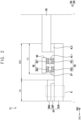
- FIG. 1 is a plan view illustrating a display device according to an embodiment.
- FIG. 2 is a cross-sectional view taken along line I-I' of FIG. 1 .
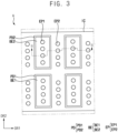
- FIG. 3 is an enlarged plan view of an example of area A of FIG. 1 .
- a display device DD may include a display panel DP, a plurality of pad electrodes PD, a driving chip IC, a plurality of elastic protrusions BP, a circuit board CB, a first adhesive layer AL1, and a second adhesive layer AL2.
- the display panel DP includes a substrate SUB, a display portion DSP disposed in the display area DA on the substrate SUB, and an encapsulation layer ENC disposed on the display portion DSP and at least partially surrounding the display portion DSP A detailed description of components of the display panel DP will be described later.
- the substrate SUB may include a display area DAand a non-display area NDA.
- the non-display area NDA may be proximate to the display area DA.
- the non-display area NDA may surround at least a portion of the display area DA.
- the display area DA may be an area capable of displaying an image by generating light or adjusting transmittance of light provided from an external light source.
- the non-display area NDA may be an area not displaying an image.
- a plurality of pixels PX may be arranged in the display area DA on the substrate SUB.
- Each of the pixels PX may include a driving element and a light emitting element electrically connected to the driving element.
- Each of the pixels PX may generate light according to a driving signal.
- the pixels PX may be entirely arranged in the display area DA in a matrix form. Signal lines providing gate signals, data signals, and the like and power supply lines providing power to each of the pixels PX may be disposed in the display area DA on the substrate SUB.
- Drivers may be disposed in the non-display area NDA.
- the drivers may include a gate driver generating the gate signal and a data driver generating the data signal.
- the non-display area NDA may include a bending area BA and a pad area PA.
- the bending area BA may be positioned between the display area DA and the pad area PA, in a plan view.
- a portion of the substrate SUB overlapping the bending area BA may be bent about a bending axis extending in the first direction DR1.
- the pad area PA may have a shape extending along one side of the display device DD.
- the pad area PA may have a shape extending along the first direction DR1 parallel to an upper surface of the substrate SUB.
- the plurality of pad electrodes PD may be disposed in the pad area PA on the substrate SUB. As shown in FIG. 3 , the pad electrodes PD may be spaced apart from each other along the first direction DR1. In addition, each of the pad electrodes PD may extend in a second direction DR2 crossing the first direction DR1. Each of the pad electrodes PD may include metal, a transparent conductive material, and the like.
- each of the pad electrodes PD may include metal such as gold (“Au”), silver (“Ag”), aluminum (“Al”), copper (“Cu”), and the like and transparent conductive material such as indium tin oxide (“ITO”), indium zinc oxide (“IZO”), indium zinc tin oxide (“IZTO”), and the like. These may be used alone or in combination with each other.
- ITO indium tin oxide
- IZO indium zinc oxide
- IZTO indium zinc tin oxide
- each of the pad electrodes PD may have a multilayer structure including ITO/Ag/ITO.
- the pad electrodes PD may include a plurality of input pad electrodes PD1 and a plurality of output pad electrodes PD2.
- the output pad electrodes PD2 may be repeatedly arranged along the first direction DR1 in a first row
- the input pad electrodes PD1 may be repeatedly arranged along the first direction DR1 in a second row adjacent to the first row.
- Each of the input pad electrode PD1 and the output pad electrode PD2 may be referred to as a pad electrode.
- the output pad electrodes PD2 may receive a driving signal output from the driving chip IC.
- the driving signal output from the driving chip IC may be provided to the pixels PX through the output pad electrodes PD2.
- the input pad electrodes PD1 may transmit control signal, power, and the like provided from the circuit board CB to the driving chip IC.
- control signal and power output from the circuit board CB may be provided to the driving chip IC through the input pad electrodes PD1
- the driving chip IC may be disposed in the pad area PA on the substrate SUB.
- the driving chip IC may control signals and voltages provided to the pixels PX.
- the driving chip IC when the substrate SUB includes glass, the driving chip IC may have a chip on glass ("COG") structure directly disposed on the substrate SUB.
- the driving chip IC when the substrate SUB includes a transparent resin substrate, the driving chip IC may have a chip on plastic (“COP”) structure directly disposed on the substrate SUB.
- COG chip on glass
- COG chip on glass
- COP chip on plastic
- the present disclosure is not necessarily limited thereto, and a flexible film is disposed in the pad area PA on the substrate SUB, and the driving chip IC may have a chip on film (COF) structure directly disposed on the flexible film.
- the driving chip IC may include a base portion BS facing the substrate SUB and a plurality of bump electrodes BE attached to a lower surface of the base portion BS.
- the bump electrodes BE may be spaced apart from each other along the first direction DR1.
- each of the bump electrodes BE may extend in the second direction DR2 crossing the first direction DR1.
- Each of the bump electrodes BE may overlap each of the pad electrodes PD.
- each of the bump electrodes BE may include a metal such as copper, gold, and the like. These may be used alone or in combination with each other.
- the base part BS may include plastic such as polyimide.
- the bump electrodes BE may include a plurality of input bump electrodes BE1 and a plurality of output bump electrodes BE2.
- the output bump electrodes BE2 may be repeatedly arranged along the first direction DR1 in the first row
- the input bump electrodes BE1 may be repeatedly arranged along the first direction DR1 in a second row adjacent to the first row.
- Each of the input bump electrode BE1 and the output bump electrode BE2 may be referred to as a bump electrode.
- Each of the output bump electrodes BE2 may output the driving signal provided to the pixels PX.
- Each of the output bump electrodes BE2 may overlap each of the output pad electrodes PE2 to correspond to each other.
- Each of the input bump electrodes BE1 may receive the control signal, the power, and the like provided from the circuit board CB. Each of the input bump electrodes BE1 may overlap each of the input pad electrodes PD1 to correspond to each other.
- the plurality of elastic protrusions EP may be disposed in the pad area PA between the substrate SUB and the driving chip IC.
- each of the elastic protrusions EP may be disposed between the pad electrode PD and the bump electrode BE.
- the pad electrode PD and the bump electrode BE may be electrically connected through the elastic protrusions EP.
- the elastic protrusions EP may electrically connect the display panel DP and the driving chip IC.
- Each of the elastic protrusions EP may include an organic polymer material.
- each of the elastic projections EP may include an organic polymer material such as an epoxy resin, an acrylic resin, a urethane resin, a photoresist, and the like. These may be used alone or in combination with each other. A detailed description of the elastic protrusions EP will be described later.
- the first adhesive layer AL1 may be disposed in the pad area PA between the substrate SUB and the driving chip IC.
- the first adhesive layer AL1 may cover the pad electrodes PD and the bump electrodes BE.
- the first adhesive layer AL1 may bond the pad electrodes PD and the driving chip IC.
- the first adhesive layer AL1 may bond the display panel DP and the driving chip IC.
- the first adhesive layer AL1 may include insulating polymer material such as an insulating polymer material.
- the first adhesive layer AL1 may include an epoxy resin, an acrylic resin, a phenol resin, a melamine resin, a diallylphthalate resin, a urea resin, a polyimide resin, a polystyrene resin, a polyurethane resin, a polyethylene resin, a polyvinyl acetate resin, and the like. These may be used alone or in combination with each other.
- the circuit board CB may be disposed in the pad area PA on the substrate SUB.
- the circuit board CB may partially overlap the pad area PA.
- a first portion of the circuit board CB may overlap the pad area PA, and a second portion of the circuit board CB might not overlap the pad area PA.
- the circuit board CB may be bonded to the substrate SUB through the second adhesive layer AL2. Accordingly, the circuit board CB may be electrically connected to the display panel DP
- the second adhesive layer AL2 may include the same material as the first adhesive layer AL1.
- the pixels PX may receive the driving signal, the control signal, and the power from the circuit board CB.
- the circuit board CB may include a printed circuit board ("PCB”), a flexible printed circuit board (“FPCB”) or a flexible flat cable (“FFC”).
- the first direction DR1 and the second direction DR2 crossing the first direction DR1 may define a plane.
- the second direction DR2 may be perpendicular to the first direction DR1.
- the display device DD of the present disclosure may include an organic light emitting diode (“OLED”) display device, a liquid crystal display (“LCD”) device, a field emission display (“FED”) device, a plasma display panel (“PDP”) device, an electrophoretic image display (“EPD”) device, or a quantum dot display device.
- OLED organic light emitting diode
- LCD liquid crystal display
- FED field emission display
- PDP plasma display panel
- EPD electrophoretic image display
- quantum dot display device a quantum dot display device.
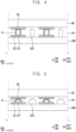
- FIG. 4 is a cross-sectional view illustrating an example of a cross section cut along line II-II' of FIG. 3 .
- FIGS. 5 , 6, 7 , and 8 are cross-sectional views illustrating examples of cross-sections taken along line II-II' of FIG. 3 .
- the plurality of pad electrodes PD, the plurality of elastic protrusions EP, the first adhesive layer AL1, and the driving chip (IC) may be disposed on the substrate SUB.
- the elastic protrusions EP may include a plurality of first elastic protrusions EP1 and a plurality of second elastic protrusions EP2.
- the first elastic protrusions EP1 may be disposed on each of the pad electrodes PD.
- a plurality of first elastic protrusions EP1 may be disposed on one pad electrode PD.
- the second elastic protrusions EP2 may be disposed between the pad electrodes PD on the substrate SUB.
- the number of first elastic protrusions EP1 disposed on one pad electrode PD may be equal to the number of the second elastic protrusions EP2 disposed adjacent two pad electrodes (e.g., the input pad electrodes PD1 or the output pad electrodes PD2).
- the number of the first elastic protrusions EP1 disposed on one pad electrode PD may be four, and the number of the second elastic protrusions EP2 disposed between the two adjacent pad electrodes may be four.
- the number of the first elastic protrusions EP1 disposed on one pad electrode PD may be different from the number of the second elastic protrusions EP2 disposed between the two adjacent pad electrodes.
- Each of the first elastic protrusions EP1 may overlap a central portion of each of the pad electrodes PD, and each of the second elastic protrusions EP2 may overlap a central portion between two adjacent pad electrodes (e.g., the input pad electrodes PD1 or the output pad electrodes PD2).
- the first elastic protrusions EP1 may be repeatedly arranged along the second direction DR2 to overlap the central portion of each of the pad electrodes PD
- the second elastic protrusions EP2 may be repeatedly arranged along the second direction DR2 to overlap the central portion between the two adjacent pad electrodes.
- each of the first elastic protrusions EP1 and the shape of each of the second elastic protrusions EP2 may be the same.
- each of the elastic protrusions EP may have a rectangular shape with rounded corners when viewed in a cross-section (see FIG. 4 ).
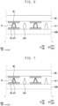
- each of the elastic protrusions EP may have a semicircular shape when viewed in a cross-section (see FIG. 5 ).
- each of the elastic protrusions EP may have a semielliptical shape when viewed in a cross-section (see FIG. 6 ).
- each of the elastic protrusions EP may have a triangular shape when viewed in a cross-section (see FIG. 7 ).
- each of the elastic protrusions EP may have a rectangular shape with one rounded side when viewed in a cross-section (see FIG. 8 ).
- the configuration of the present disclosure is not necessarily limited thereto, and each of the elastic protrusions EP may have various shapes when viewed in a cross-section.
- the display device DD may further include a conductive layer CL disposed on each of the first elastic protrusions EP1.
- the conductive layer CL may at least partially surround an outer surface of each of the first elastic protrusions EP1. At this time, the outer surface of each of the second elastic protrusions EP2 may be exposed.
- the conductive layer CL may include a metal, an alloy metal nitride, a conductive metal oxide, a transparent conductive material, and the like. These may be used alone or in combination with each other.
- an upper surface of the conductive layer CL may be positioned at the same level as an upper surface of each of the second elastic protrusions EP2.
- the conductive layer CL may include the same material as a source electrode (e.g., the source electrode SE of FIG. 11 ) and a drain electrode (e.g., the drain electrode DE of FIG. 11 ).
- the conductive layer CL may be formed through the same process as the source electrode and the drain electrode.
- the configuration of the present disclosure is not necessarily limited thereto, and the conductive layer CL may include the same material as the metal layer disposed on a different layer from the source electrode and the drain electrode.
- Each of the bump electrodes BE may contact the upper surface of the conductive layer CL and might not contact the second elastic protrusions EP2.
- the pad electrodes PD and the bump electrodes BE may be electrically connected through the conductive layer CL.
- the substrate SUB and the driving chip IC may be electrically connected through the conductive layer CL.
- each of the bump electrodes BE may at least partially contact the upper surface of the conductive layer CL and at least partially overlap the upper surface of each of the second elastic protrusions EP2.
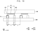
- FIGS. 9 and 10 are cross-sectional views illustrating the relationship between a width of a bump electrode, a width of an elastic protrusion, and a gap between adjacent elastic protrusions of FIG. 4 .
- FIG. 9 is a cross-sectional view illustrating a state in which the driving chip IC is aligned on the substrate SUB
- FIG. 10 is a cross-sectional view illustrating a state in which the driving chip IC is shifted by a predetermined distance x in the first direction DR1 from a desired position on the substrate SUB.
- a width W1 of each of the first elastic protrusions EP1 may equal to the width W1 of each of the second elastic protrusions EP2.
- each of the width W1 of the first elastic protrusion EP1 and the width W1 of the second elastic protrusion EP2 may mean a width in the first direction DR1.
- the elastic protrusions EP when viewed in a cross-section, may be spaced apart from each other at equal distance d along the first direction DR1.
- the distance d between the first elastic protrusion EP1 positioned in a first column and the second elastic protrusion EP2 positioned in the second column adjacent to the first column may be equal to the distance d between the second elastic protrusion EP2 positioned in the second row and the first elastic protrusion EP1 positioned in a third row adjacent to the second row.
- a width W2 of each of the bump electrodes BE may be N times the sum of the width W1 of each elastic protrusion EP and the distance d between two adjacent elastic protrusions EP in the first direction DR1 (where the N is a positive integer).
- the width W2 of each of the bump electrodes BE may equal to the sum of the width W1 of each elastic protrusion EP and the distance d between two adjacent elastic protrusions EP in the first direction DR1.
- the sum of the widths of the portions where each of the bump electrodes BE overlaps the elastic protrusions BP may be N times the width W1 of each of the elastic protrusions BP (where, the N is a positive integer).
- the width W1 of the portion where each of the bump electrodes BE overlaps the first elastic protrusion EP1 may be equal to the width W1 of each of the elastic protrusions EP1.
- the sum of the width (e.g., a difference between the width W1 of the first elastic protrusion EP1 and the distance x shifted at the desired position of the driving chip IC) of the portion where each of the bump electrodes BE overlaps the first elastic protrusion BP1 and the width x of the portion where each of the bump electrodes BE overlaps the second elastic protrusion BP2 may be equal to the width W1 of each of the elastic protrusions EP.
- the magnitude of the pressure pressing the substrate SUB in a state where driving chip IC is aligned on the substrate SUB may be the same as the magnitude of the pressure pressing the substrate SUB in a state where the driving chip IC is shifted from the desired position.
- a driving chip may be bonded to a display panel through an anisotropic conductive film ("ACF") including an adhesive layer and a plurality of conductive balls arranged in the adhesive layer.
- ACF anisotropic conductive film
- the conductive balls are concentrated on the side surfaces of the electrodes, a short defect occurred between the adjacent electrodes, or since the conductive balls are properly disposed between the electrodes, an open defect occurred.
- the display device DD may include the plurality of pad electrodes PD disposed in the pad area PA on a substrate SUB, the plurality of first elastic protrusions EP1 disposed on each of the pad electrodes PD, the plurality of second elastic protrusions EP2 disposed between the pad electrodes PD on the substrate SUB when viewed from in a plan view, and the driving chip IC.
- the driving chip IC may include the base portion BS facing the substrate SUB and the plurality of bump electrodes BE attached to the lower surface of the base portion BS.
- the width W2 of each of the bump electrodes BE may be N times the sum of the width W1 of each elastic protrusion EP and the distance d between two adjacent elastic protrusions EP (where the N is a positive integer). Accordingly, a short defect or an open defect of the display device DD occurring in the process of bonding the driving chip IC to the substrate SUB may be reduced in frequency and/or severity.
- FIG. 11 is an enlarged cross-sectional view of area B of FIG. 2 .
- the display panel DP of the display device DD may include the substrate SUB, the display portion DSP disposed on the substrate SUB, and the encapsulation layer ENC disposed on the display portion DSP
- the display portion DSP may include a buffer layer BUF, a transistor TR, a first insulating layer IL1, a second insulating layer IL2, a third insulating layer IL3, a pixel defining layer PDL, and a light emitting element LED.
- the transistor TR may include an active pattern ACT, a gate electrode GAT, a source electrode SE, and a drain electrode DE, and the light emitting element LED may include an anode electrode ADE, a light emitting layer EL, and a cathode electrode CTE.
- the substrate SUB may include a transparent material or an opaque material.
- the substrate SUB may be made of a transparent resin substrate.
- An example of a transparent resin substrate that can be used as the substrate SUB may include a polyimide substrate.
- the polyimide substrate may include a first polyimide layer, a barrier film layer, and a second polyimide layer.
- the substrate SUB may include a quartz substrate, a synthetic quartz substrate, a calcium fluoride substrate, an F-doped quartz substrate, soda lime glass substrate, a non-alkali glass substrate, and the like. These may be used alone or in combination with each other.
- the buffer layer BUF may be disposed on the substrate SUB.
- the buffer layer BUF may prevent diffusion of metal atoms or impurities from the substrate SUB into the transistor TR.
- the buffer layer BUF may increase flatness of the surface of the substrate SUB when the surface of the substrate SUB is not uniform.
- the buffer layer BUF may include an inorganic material such as silicon oxide, silicon nitride, silicon oxynitride, and the like. These may be used alone or in combination with each other.
- the active pattern ACT may be disposed on the buffer layer BUF.
- the active pattern ACT may include a metal oxide semiconductor, an inorganic semiconductor (e.g., amorphous silicon, poly silicon), or an organic semiconductor.
- the active pattern ACT may include a source region, a drain region, and a channel region positioned between the source region and the drain region.
- the metal oxide semiconductor may include a two-component compound ("AB x "), a ternary compound (“AB x C y “), a four-component compound (“AB x C y D z “), and the like containing indium (“In”), zinc (“Zn”), gallium (“Ga”), tin (“Sn”), titanium (“Ti”), aluminum (“Al”), hafnium (“Hf'), zirconium (“Zr”), magnesium (“Mg”), and the like.
- the metal oxide semiconductor may include zinc oxide ("ZnO x "), gallium oxide (“GaO x “), tin oxide (“SnO x “), indium oxide ("InO x “), indium gallium oxide (“IGO”), indium zinc oxide (“IZO”), indium tin oxide (“ITO”), indium zinc tin oxide (“IZTO”), indium gallium zinc oxide (“IGZO”), and the like. These may be used alone or in combination with each other.
- the first insulating layer IL1 may be disposed on the buffer layer BUF.
- the first insulating layer IL1 may sufficiently cover the active pattern ACT, and may have a substantially flat upper surface without creating a step around the active pattern ACT.
- the first insulating layer IL1 may cover the active pattern ACT and may be disposed along the profile of the active pattern ACT with a uniform thickness.
- the first insulating layer IL1 may include an inorganic material such as silicon oxide (“SiO x "), silicon nitride (“SiN x “), silicon carbide (“SiC x “), silicon oxynitride (“SiO x N y “), silicon oxycarbide (“SiO x C y “), and the like. These may be used alone or in combination with each other.
- the gate electrode GAT may be disposed on the first insulating layer IL1.
- the gate electrode GAT may overlap the channel region of the active pattern ACT.
- the gate electrode GAT may include a metal, an alloy metal nitride, a conductive metal oxide, a transparent conductive material, and the like.
- the metal may include silver ("Ag”), molybdenum (“Mo”), aluminum (“Al”), tungsten ("W”), copper (“Cu”), nickel (“Ni”), chromium (“Cr”), titanium (“Ti”), tantalum (“Ta”), platinum (“Pt”), scandium (“Sc”), and the like.
- the conductive metal oxide may include indium tin oxide, indium zinc oxide, and the like.
- examples of the metal nitride may include aluminum nitride ("AlN x "), tungsten nitride (“WN x “), chromium nitride (“CrN x “), and the like. These may be used alone or in combination with each other.
- the second insulating layer IL2 may be disposed on the first insulating layer IL 1.
- the second insulating layer IL2 may sufficiently cover the gate electrodes GAT, and may have a substantially flat upper surface without creating a step around the gate electrodes GAT.
- the second insulating layer IL2 may cover the gate electrode GAT and may be disposed along the profile of each gate electrode GAT with a uniform thickness.
- the second insulating layer IL2 may include an inorganic material such as silicon oxide, silicon nitride, silicon carbide, silicon oxynitride, silicon oxycarbide, and the like. These may be used alone or in combination with each other.
- the source electrode SE and the drain electrode DE may be disposed on the interlayer insulating layer ILD.
- the source electrode SE1 may be connected to the source region of the active pattern ACT through a contact hole passing through a first portion of the first insulating layer IL1 and the second insulating layer IL2.
- the drain electrode may be connected to the drain region of the active pattern ACT through a contact hole passing through a second portion of the first insulating layer IL1 and the second insulating layer IL2.
- each of the source electrode SE and the drain electrode DE may include a metal, an alloy, a metal nitride, a conductive metal oxide, a transparent conductive material, and the like. These may be used alone or in combination with each other.
- the transistor TR including the active pattern ACT, the gate electrode GAT, the source electrode SE, and the drain electrode DE may be disposed on the substrate SUB in the display area DA.
- the third insulating layer IL3 may be disposed on the second insulating layer IL2.
- the third insulating layer IL3 may sufficiently cover the source electrode SE and the drain electrode DE.
- the third insulating layer IL3 may include an inorganic material or an organic material.
- the third insulating layer IL3 may include an organic material such as phenolic resin, polyacrylates resin, polyimides rein, polyamides resin, siloxane resin, epoxy resin, and the like. These may be used alone or in combination with each other.
- the anode electrode ADE may be disposed on the third insulating layer IL3.
- the anode electrode ADE may be connected to the drain electrode DE of the transistor TR through a contact hole passing through the third insulating layer IL3.
- the anode electrode ADE may include a metal, an alloy, a metal nitride, a conductive metal oxide, a transparent conductive material, and the like. These may be used alone or in combination with each other.
- the anode electrode ADE may have a stacked structure including ITO/Ag/ITO.
- the pixel defining layer PDL may be disposed on the third insulating layer IL3.
- the pixel defining layer PDL may cover both sides of the anode electrode ADE.
- the pixel defining layer PDL may include an organic material or an organic material.
- the pixel defining layer PDL may include an organic material such as an epoxy resin, a siloxane resin, and the like. These may be used alone or in combination with each other.
- the pixel defining layer PDL may further include a light blocking material containing a black pigment, black dye, and the like.
- the light emitting layer EL may be disposed on the anode electrode ADE.
- the light emitting layer EL may include an organic material that emits light of a predetermined color.
- the light emitting layer EL may include an organic material that emits red light, green light, or blue light.
- the cathode electrode CTE may be disposed on the light emitting layer EL and the pixel defining layer PDL.
- the cathode electrode CTE may include a metal, an alloy, a metal nitride, a conductive metal oxide, a transparent conductive material, and the like. These may be used alone or in combination with each other.
- the light emitting element LED including the anode electrode ADE, the light emitting layer EL, and the cathode electrode CTE may be disposed in the display area DA on the substrate SUB.
- the encapsulation layer ENC may be disposed on the cathode electrode CTE.
- the encapsulation layer ENC may prevent impurities, moisture, air, and the like from permeating the light emitting element LED from the outside.
- the encapsulation layer ENC may include at least one inorganic layer and at least one organic layer.
- the inorganic layer may include silicon oxide, silicon nitride, silicon oxynitride, and the like. These may be used alone or in combination with each other.
- the organic layer may include a polymer cured material such as polyacrylate.
- FIG. 12 is an enlarged plan view of an example of area A of FIG. 1 .
- FIG. 13 is a cross-sectional view taken along line III-III' of FIG. 12 .
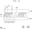
- FIGS. 14 and 15 are cross-sectional views illustrating the relationship between a width of a bump electrode, a width of an elastic protrusion, and a gap between adjacent elastic protrusions of FIG. 13 .
- FIG. 14 is a cross-sectional view illustrating a state in which the driving chip IC is aligned on the substrate SUB
- FIG. 15 is a cross-sectional view illustrating a state in which the driving chip IC is shifted by a predetermined distance x in the first direction DR1 from a desired position on the substrate SUB.
- the plurality of pad electrodes PD, the plurality of elastic protrusions BP, the first adhesive layer AL1, and the driving chip IC may be disposed in the pad area PA on the substrate SUB.
- the display device described with reference to FIGS. 12 , 13 , 14 , and 15 may be substantially the same as or similar to the display device DD described with reference to FIGS. 3 , 4 , 5 , 6 , 7 , 8 , 9 , and 10 except for the number of the elastic protrusions EP.
- the element is at least similar to a corresponding element that has been described elsewhere within the present disclosure.
- the number of first elastic protrusions EP1 disposed on one pad electrode PD may be equal to the number of the second elastic protrusions EP2 disposed adjacent two pad electrodes (e.g., the input pad electrodes PD1 or the output pad electrodes PD2).
- the number of the first elastic protrusions EP1 disposed on one pad electrode PD may be eight, and the number of the second elastic protrusions EP2 disposed between the two adjacent pad electrodes may be eight.
- the number of the first elastic protrusions EP1 disposed on one pad electrode PD may be different from the number of the second elastic protrusions EP2 disposed between the two adjacent pad electrodes.
- the first elastic protrusions EP1 may be arranged in a first zigzag pattern
- the second elastic protrusions EP2 may be arranged in a second zigzag pattern.
- the arrangement method of the first elastic protrusions EP1 and the arrangement method of the second elastic protrusions EP2 may be the same.
- the configuration of the present disclosure is not necessarily limited thereto, and the arrangement method of the first elastic protrusions EP1 and the arrangement method of the second elastic protrusions EP2 may be different in a plan view.
- the width W1 of each of the first elastic protrusions EP1 may be equal to the width W1 of each of the second elastic protrusions EP2.
- the elastic protrusions EP when viewed in a cross-section, may be spaced apart from each other at equal distance d along the first direction DR1.
- a width W2 of each of the bump electrodes BE may be N times the sum of the width W1 of each elastic protrusion EP and the distance d between two adjacent elastic protrusions EP in the first direction DR1 (where the N is a positive integer).
- the width W2 of each of the bump electrodes BE may be twice the sum of the width W1 of each elastic protrusion EP and the distance d between two adjacent elastic protrusions EP in the first direction DR1.
- the sum of the widths of the portions where each of the bump electrodes BE overlaps the elastic protrusions BP may be N times the width W1 of each of the elastic protrusions BP (where, the N is a positive integer).
- the width W1 of the portion where each of the bump electrodes BE overlaps the first elastic protrusion EP1 may be two times the width W1 of each of the elastic protrusions EP1.
- the sum of the width of the portion where each of the bump electrodes BE overlaps the first elastic protrusion BP1 and the width x of the portion where each of the bump electrodes BE overlaps the second elastic protrusion BP2 may be two times the width W1 of each of the elastic protrusions EP.
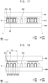
- FIG. 16 is an enlarged plan view of an example of area A of FIG. 1 .
- FIG. 17 is a cross-sectional view taken along line IV-IV' of FIG. 16 .
- FIGS. 18 and 19 are cross-sectional views illustrating the relationship between a width of a bump electrode, a width of an elastic protrusion, and a gap between adjacent elastic protrusions of FIG. 17 .
- FIG. 18 is a cross-sectional view illustrating a state in which the driving chip IC is aligned on the substrate SUB
- FIG. 19 is a cross-sectional view illustrating a state in which the driving chip IC is shifted by a predetermined distance x in the first direction DR1 from a desired position on the substrate SUB.
- the plurality of pad electrodes PD, the plurality of elastic protrusions BP, the first adhesive layer AL1, and the driving chip IC may be disposed in the pad area PA on the substrate SUB.
- the display device described with reference to FIGS. 16 , 17 , 18 , and 19 may be substantially the same as or similar to the display device DD described with reference to FIGS. 3 , 4 , 5 , 6 , 7 , 8 , 9 , and 10 except for the number of the elastic protrusions EP.
- the element is at least similar to a corresponding element that has been described elsewhere within the present disclosure.
- the number of first elastic protrusions EP1 disposed on one pad electrode PD may be equal to the number of the second elastic protrusions EP2 disposed adjacent two pad electrodes (e.g., the input pad electrodes PD1 or the output pad electrodes PD2).
- the number of the first elastic protrusions EP1 disposed on one pad electrode PD may be twelve, and the number of the second elastic protrusions EP2 disposed between the two adjacent pad electrodes may be twelve.
- the number of the first elastic protrusions EP1 disposed on one pad electrode PD may be different from the number of the second elastic protrusions EP2 disposed between the two adjacent pad electrodes.
- the first elastic protrusions EP1 may be arranged in a first zigzag pattern
- the second elastic protrusions EP2 may be arranged in a second zigzag pattern.
- the arrangement method of the first elastic protrusions EP1 and the arrangement method of the second elastic protrusions EP2 may be the same.
- the configuration of the present disclosure is not necessarily limited thereto, and the arrangement method of the first elastic protrusions EP1 and the arrangement method of the second elastic protrusions EP2 may be different, in a plan view.
- the width W1 of each of the first elastic protrusions EP1 may be equal to the width W1 of each of the second elastic protrusions EP2.
- the elastic protrusions EP when viewed in a cross-section, may be spaced apart from each other at equal distance d along the first direction DR1.
- a width W2 of each of the bump electrodes BE may be N times the sum of the width W1 of each elastic protrusion EP and the distance d between two adjacent elastic protrusions EP in the first direction DR1 (where the N is a positive integer).
- the width W2 of each of the bump electrodes BE may be three times the sum of the width W1 of each elastic protrusion EP and the distance d between two adjacent elastic protrusions EP in the first direction DR1.
- the sum of the widths of the portions where each of the bump electrodes BE overlaps the elastic protrusions BP may be N times the width W1 of each of the elastic protrusions BP (where, the N is a positive integer).
- the width W1 of the portion where each of the bump electrodes BE overlaps the first elastic protrusion EP1 may be three times the width W1 of each of the elastic protrusions EP1.
- the sum of the width of the portion where each of the bump electrodes BE overlaps the first elastic protrusion BP1 and the width x of the portion where each of the bump electrodes BE overlaps the second elastic protrusion BP2 may be three times the width W1 of each of the elastic protrusions EP.
- the present disclosure can be applied to various display devices.
- the present disclosure is applicable to various display devices such as display devices for vehicles, ships and aircraft, portable communication devices, display devices for exhibition or information transmission, medical display devices, and the like.
Landscapes
- Physics & Mathematics (AREA)
- Engineering & Computer Science (AREA)
- Microelectronics & Electronic Packaging (AREA)
- Nonlinear Science (AREA)
- Mathematical Physics (AREA)
- Chemical & Material Sciences (AREA)
- Crystallography & Structural Chemistry (AREA)
- General Physics & Mathematics (AREA)
- Optics & Photonics (AREA)
- Geometry (AREA)
- Devices For Indicating Variable Information By Combining Individual Elements (AREA)
Applications Claiming Priority (1)
| Application Number | Priority Date | Filing Date | Title |
|---|---|---|---|
| KR1020220113832A KR20240034970A (ko) | 2022-09-07 | 2022-09-07 | 표시 장치 |
Publications (1)
| Publication Number | Publication Date |
|---|---|
| EP4336989A1 true EP4336989A1 (de) | 2024-03-13 |
Family
ID=87575996
Family Applications (1)
| Application Number | Title | Priority Date | Filing Date |
|---|---|---|---|
| EP23191240.3A Pending EP4336989A1 (de) | 2022-09-07 | 2023-08-14 | Anzeigevorrichtung mit elastischen vorsprüngen auf der pad-fläche eines substrats |
Country Status (4)
| Country | Link |
|---|---|
| US (1) | US20240081112A1 (de) |
| EP (1) | EP4336989A1 (de) |
| KR (1) | KR20240034970A (de) |
| CN (1) | CN117677236A (de) |
Citations (5)
| Publication number | Priority date | Publication date | Assignee | Title |
|---|---|---|---|---|
| US20050098901A1 (en) * | 2003-11-06 | 2005-05-12 | Shyh-Ming Chang | Bonding structure with compliant bumps |
| US20060146214A1 (en) * | 2002-12-09 | 2006-07-06 | Seong-Yong Hwang | Thin film transistor substrate, method of manufacturing the same, liquid crystal display apparatus having the same and method of manufacturing the liquid crystal display apparatus |
| US20090039495A1 (en) * | 2005-10-05 | 2009-02-12 | Sharp Kabushiki Kaisha | Wiring substrate and display device including the same |
| US20130335940A1 (en) * | 2011-03-04 | 2013-12-19 | Sharp Kabushiki Kaisha | Electronic circuit substrate, display device, and wiring substrate |
| US20190348487A1 (en) * | 2018-05-10 | 2019-11-14 | Samsung Display Co., Ltd. | Display device |
-
2022
- 2022-09-07 KR KR1020220113832A patent/KR20240034970A/ko active Pending
-
2023
- 2023-05-24 US US18/322,959 patent/US20240081112A1/en active Pending
- 2023-08-14 EP EP23191240.3A patent/EP4336989A1/de active Pending
- 2023-08-28 CN CN202311085916.7A patent/CN117677236A/zh active Pending
Patent Citations (5)
| Publication number | Priority date | Publication date | Assignee | Title |
|---|---|---|---|---|
| US20060146214A1 (en) * | 2002-12-09 | 2006-07-06 | Seong-Yong Hwang | Thin film transistor substrate, method of manufacturing the same, liquid crystal display apparatus having the same and method of manufacturing the liquid crystal display apparatus |
| US20050098901A1 (en) * | 2003-11-06 | 2005-05-12 | Shyh-Ming Chang | Bonding structure with compliant bumps |
| US20090039495A1 (en) * | 2005-10-05 | 2009-02-12 | Sharp Kabushiki Kaisha | Wiring substrate and display device including the same |
| US20130335940A1 (en) * | 2011-03-04 | 2013-12-19 | Sharp Kabushiki Kaisha | Electronic circuit substrate, display device, and wiring substrate |
| US20190348487A1 (en) * | 2018-05-10 | 2019-11-14 | Samsung Display Co., Ltd. | Display device |
Also Published As
| Publication number | Publication date |
|---|---|
| CN117677236A (zh) | 2024-03-08 |
| US20240081112A1 (en) | 2024-03-07 |
| KR20240034970A (ko) | 2024-03-15 |
Similar Documents
| Publication | Publication Date | Title |
|---|---|---|
| US10998391B2 (en) | Display apparatus with a crack detection line | |
| EP3608964B1 (de) | Dehnbare anzeigevorrichtung | |
| KR102523979B1 (ko) | 표시 장치 | |
| CN113257121A (zh) | 一种显示装置及其制作方法和拼接显示装置 | |
| KR102426268B1 (ko) | 표시장치와 그의 제조방법 | |
| KR102840850B1 (ko) | 스트레쳐블 표시 장치 | |
| KR102433358B1 (ko) | 표시 장치 | |
| US12477878B2 (en) | Display device | |
| CN116390536A (zh) | 显示面板 | |
| EP4336989A1 (de) | Anzeigevorrichtung mit elastischen vorsprüngen auf der pad-fläche eines substrats | |
| US10714705B2 (en) | Organic light emitting display device | |
| KR102758302B1 (ko) | 표시장치와 그의 제조방법 | |
| KR20170079156A (ko) | 유기발광 표시장치 | |
| CN117093089A (zh) | 具有触摸传感器的显示装置 | |
| CN223007850U (zh) | 显示装置 | |
| JP7654044B2 (ja) | フレキシブル表示装置 | |
| EP4641349A1 (de) | Anzeigevorrichtung und elektronische vorrichtung | |
| US12446397B2 (en) | Display panel including conductive side cover | |
| US20240081114A1 (en) | Display device | |
| KR102863918B1 (ko) | 표시 패널 및 표시 패널의 제조 방법 | |
| JP2003280539A (ja) | 有機el表示装置 | |
| US20240304610A1 (en) | Display device | |
| KR102925292B1 (ko) | 표시 장치 | |
| CN119947470A (zh) | 显示装置 | |
| CN120390545A (zh) | 显示装置 |
Legal Events
| Date | Code | Title | Description |
|---|---|---|---|
| PUAI | Public reference made under article 153(3) epc to a published international application that has entered the european phase |
Free format text: ORIGINAL CODE: 0009012 |
|
| STAA | Information on the status of an ep patent application or granted ep patent |
Free format text: STATUS: THE APPLICATION HAS BEEN PUBLISHED |
|
| AK | Designated contracting states |
Kind code of ref document: A1 Designated state(s): AL AT BE BG CH CY CZ DE DK EE ES FI FR GB GR HR HU IE IS IT LI LT LU LV MC ME MK MT NL NO PL PT RO RS SE SI SK SM TR |
|
| STAA | Information on the status of an ep patent application or granted ep patent |
Free format text: STATUS: REQUEST FOR EXAMINATION WAS MADE |
|
| 17P | Request for examination filed |
Effective date: 20240327 |
|
| RBV | Designated contracting states (corrected) |
Designated state(s): AL AT BE BG CH CY CZ DE DK EE ES FI FR GB GR HR HU IE IS IT LI LT LU LV MC ME MK MT NL NO PL PT RO RS SE SI SK SM TR |
|
| P01 | Opt-out of the competence of the unified patent court (upc) registered |
Free format text: CASE NUMBER: UPC_APP_0007185_4336989/2026 Effective date: 20260226 |