EP4339749A1 - Anzeigevorrichtung - Google Patents
Anzeigevorrichtung Download PDFInfo
- Publication number
- EP4339749A1 EP4339749A1 EP22845124.1A EP22845124A EP4339749A1 EP 4339749 A1 EP4339749 A1 EP 4339749A1 EP 22845124 A EP22845124 A EP 22845124A EP 4339749 A1 EP4339749 A1 EP 4339749A1
- Authority
- EP
- European Patent Office
- Prior art keywords
- module
- isolation structure
- display device
- display
- touch module
- Prior art date
- Legal status (The legal status is an assumption and is not a legal conclusion. Google has not performed a legal analysis and makes no representation as to the accuracy of the status listed.)
- Granted
Links
Images



Classifications
-
- H—ELECTRICITY
- H05—ELECTRIC TECHNIQUES NOT OTHERWISE PROVIDED FOR
- H05K—PRINTED CIRCUITS; CASINGS OR CONSTRUCTIONAL DETAILS OF ELECTRIC APPARATUS; MANUFACTURE OF ASSEMBLAGES OF ELECTRICAL COMPONENTS
- H05K5/00—Casings, cabinets or drawers for electric apparatus
- H05K5/0017—Casings, cabinets or drawers for electric apparatus with operator interface units
- H05K5/0018—Casings, cabinets or drawers for electric apparatus with operator interface units having an electronic display
-
- G—PHYSICS
- G06—COMPUTING OR CALCULATING; COUNTING
- G06F—ELECTRIC DIGITAL DATA PROCESSING
- G06F1/00—Details not covered by groups G06F3/00 - G06F13/00 and G06F21/00
- G06F1/16—Constructional details or arrangements
- G06F1/1613—Constructional details or arrangements for portable computers
- G06F1/1626—Constructional details or arrangements for portable computers with a single-body enclosure integrating a flat display, e.g. Personal Digital Assistants [PDAs]
-
- G—PHYSICS
- G06—COMPUTING OR CALCULATING; COUNTING
- G06F—ELECTRIC DIGITAL DATA PROCESSING
- G06F1/00—Details not covered by groups G06F3/00 - G06F13/00 and G06F21/00
- G06F1/16—Constructional details or arrangements
- G06F1/1613—Constructional details or arrangements for portable computers
- G06F1/1633—Constructional details or arrangements of portable computers not specific to the type of enclosures covered by groups G06F1/1615 - G06F1/1626
- G06F1/1637—Details related to the display arrangement, including those related to the mounting of the display in the housing
-
- G—PHYSICS
- G06—COMPUTING OR CALCULATING; COUNTING
- G06F—ELECTRIC DIGITAL DATA PROCESSING
- G06F1/00—Details not covered by groups G06F3/00 - G06F13/00 and G06F21/00
- G06F1/16—Constructional details or arrangements
- G06F1/1613—Constructional details or arrangements for portable computers
- G06F1/1633—Constructional details or arrangements of portable computers not specific to the type of enclosures covered by groups G06F1/1615 - G06F1/1626
- G06F1/1637—Details related to the display arrangement, including those related to the mounting of the display in the housing
- G06F1/1643—Details related to the display arrangement, including those related to the mounting of the display in the housing the display being associated to a digitizer, e.g. laptops that can be used as penpads
-
- G—PHYSICS
- G06—COMPUTING OR CALCULATING; COUNTING
- G06F—ELECTRIC DIGITAL DATA PROCESSING
- G06F1/00—Details not covered by groups G06F3/00 - G06F13/00 and G06F21/00
- G06F1/16—Constructional details or arrangements
- G06F1/1613—Constructional details or arrangements for portable computers
- G06F1/1633—Constructional details or arrangements of portable computers not specific to the type of enclosures covered by groups G06F1/1615 - G06F1/1626
- G06F1/1656—Details related to functional adaptations of the enclosure, e.g. to provide protection against EMI, shock, water, or to host detachable peripherals like a mouse or removable expansions units like PCMCIA cards, or to provide access to internal components for maintenance or to removable storage supports like CDs or DVDs, or to mechanically mount accessories
-
- G—PHYSICS
- G06—COMPUTING OR CALCULATING; COUNTING
- G06F—ELECTRIC DIGITAL DATA PROCESSING
- G06F1/00—Details not covered by groups G06F3/00 - G06F13/00 and G06F21/00
- G06F1/16—Constructional details or arrangements
- G06F1/1613—Constructional details or arrangements for portable computers
- G06F1/1633—Constructional details or arrangements of portable computers not specific to the type of enclosures covered by groups G06F1/1615 - G06F1/1626
- G06F1/1684—Constructional details or arrangements related to integrated I/O peripherals not covered by groups G06F1/1635 - G06F1/1675
-
- G—PHYSICS
- G06—COMPUTING OR CALCULATING; COUNTING
- G06F—ELECTRIC DIGITAL DATA PROCESSING
- G06F3/00—Input arrangements for transferring data to be processed into a form capable of being handled by the computer; Output arrangements for transferring data from processing unit to output unit, e.g. interface arrangements
- G06F3/01—Input arrangements or combined input and output arrangements for interaction between user and computer
- G06F3/016—Input arrangements with force or tactile feedback as computer generated output to the user
-
- H—ELECTRICITY
- H05—ELECTRIC TECHNIQUES NOT OTHERWISE PROVIDED FOR
- H05K—PRINTED CIRCUITS; CASINGS OR CONSTRUCTIONAL DETAILS OF ELECTRIC APPARATUS; MANUFACTURE OF ASSEMBLAGES OF ELECTRICAL COMPONENTS
- H05K5/00—Casings, cabinets or drawers for electric apparatus
- H05K5/02—Details
-
- G—PHYSICS
- G06—COMPUTING OR CALCULATING; COUNTING
- G06F—ELECTRIC DIGITAL DATA PROCESSING
- G06F2203/00—Indexing scheme relating to G06F3/00 - G06F3/048
- G06F2203/041—Indexing scheme relating to G06F3/041 - G06F3/045
- G06F2203/04107—Shielding in digitiser, i.e. guard or shielding arrangements, mostly for capacitive touchscreens, e.g. driven shields, driven grounds
-
- G—PHYSICS
- G06—COMPUTING OR CALCULATING; COUNTING
- G06F—ELECTRIC DIGITAL DATA PROCESSING
- G06F3/00—Input arrangements for transferring data to be processed into a form capable of being handled by the computer; Output arrangements for transferring data from processing unit to output unit, e.g. interface arrangements
- G06F3/01—Input arrangements or combined input and output arrangements for interaction between user and computer
- G06F3/03—Arrangements for converting the position or the displacement of a member into a coded form
- G06F3/041—Digitisers, e.g. for touch screens or touch pads, characterised by the transducing means
- G06F3/0412—Digitisers structurally integrated in a display
-
- G—PHYSICS
- G06—COMPUTING OR CALCULATING; COUNTING
- G06F—ELECTRIC DIGITAL DATA PROCESSING
- G06F3/00—Input arrangements for transferring data to be processed into a form capable of being handled by the computer; Output arrangements for transferring data from processing unit to output unit, e.g. interface arrangements
- G06F3/01—Input arrangements or combined input and output arrangements for interaction between user and computer
- G06F3/03—Arrangements for converting the position or the displacement of a member into a coded form
- G06F3/041—Digitisers, e.g. for touch screens or touch pads, characterised by the transducing means
- G06F3/044—Digitisers, e.g. for touch screens or touch pads, characterised by the transducing means by capacitive means
-
- G—PHYSICS
- G09—EDUCATION; CRYPTOGRAPHY; DISPLAY; ADVERTISING; SEALS
- G09F—DISPLAYING; ADVERTISING; SIGNS; LABELS OR NAME-PLATES; SEALS
- G09F13/00—Illuminated signs; Luminous advertising
- G09F13/04—Signs, boards or panels, illuminated from behind the insignia
- G09F13/0413—Frames or casing structures therefor
-
- G—PHYSICS
- G09—EDUCATION; CRYPTOGRAPHY; DISPLAY; ADVERTISING; SEALS
- G09G—ARRANGEMENTS OR CIRCUITS FOR CONTROL OF INDICATING DEVICES USING STATIC MEANS TO PRESENT VARIABLE INFORMATION
- G09G2300/00—Aspects of the constitution of display devices
- G09G2300/04—Structural and physical details of display devices
Definitions
- the present disclosure relates to the technical field of display, and in particular to a display device.
- Haptic feedback is the focus of today's technology development, and the haptic feedback can enable a terminal to interact with the human body through the sense of touch.
- the haptic feedback may be divided into two categories: one is vibration feedback, and the other is haptic reproduction technology.
- the surface haptic reproduction technology can perceive characteristics of objects through touch of a screen by a bare finger, realize efficient and natural interaction on multimedia terminals, has great research value, and thus has been widely concerned by domestic and foreign researchers.
- the surface haptic sense is the effect of the surface roughness of the object on the surface of the skin (fingertip), and different friction forces are formed due to different surface structures. Therefore, different haptic/tactile simulations may be realized by controlling the surface friction forces.
- Embodiments of the present disclosure provide a display device, including:
- a Young's modulus of each of the first isolation structure and the second isolation structure is less than 0.1 MPa.
- a material of the first isolation structure is polydimethylsiloxane, PDMS, foam or rubber; and a material of the second isolation structure is PDMS, foam or rubber.
- the second isolation structure is located at positions of two opposite edge frames of the display module.
- the second isolation structure located at one of the positions of the two opposite edge frames includes a plurality of second isolation parts arranged at intervals.
- an extension direction of each of the two opposite edge frames where the second isolation structure is located is perpendicular to a vibration propagation direction of the standing wave.
- the two opposite edge frames where the second isolation structure is located are short edge frames.
- the second isolation structure is fixed on a surface of the display module facing the touch module.
- the module outer frame includes a module side frame and a module bottom frame, and the display opening window is located at a side facing away from the module bottom frame; and the second isolation structure is further fixed on a side of the display module facing the module side frame.
- the first isolation structure is located at positions of two opposite edge frames of the touch module; and the first isolation structure and the second isolation structure are arranged at edge frames on same sides.
- the first isolation structure located at one of the positions of the two opposite edge frames includes a plurality of first isolation parts arranged at intervals.
- the module outer frame includes a module side frame, a module bottom frame, and a module top frame
- the module top frame includes the display opening window
- the first isolation structure is fixed on a surface of the touch module facing the module top frame.
- the first isolation structure and the second isolation structure are covered by the module top frame, and the first isolation structure and the second isolation structure do not overlap with the display opening window.
- the haptic sensor is covered by the module top frame, and the haptic sensor does not overlap with the display opening window.
- the haptic sensor, the first isolation structure, and the second isolation structure are located at positions of two opposite short edge frames;
- the first isolation structure is further fixed on a side of the touch module facing the module side frame.
- the display device further includes: a limiting structure, arranged on a side of the module top frame facing the module bottom frame;
- the module outer frame includes a fixing component within the accommodating space, the fixing component is configured to fix the display module and the touch module; and the first isolation structure is arranged between the fixing component and the touch module.
- the module outer frame includes a module side frame and a module bottom frame, and the display opening window is located at a side facing away from the module bottom frame; and the first isolation structure is arranged between the touch module and the module side frame.
- the first isolation structure is arranged to surround the touch module.
- the haptic sensor and the second isolation structure are located at positions of two opposite short edge frames; and the touch module includes a light-blocking layer configured to block the haptic sensor and the second isolation structure.
- Ultrasonic haptic reproduction device uses piezoelectric elements to resonate and form standing waves, forming a pressure film effect.
- This structure only requires a planar body (such as glass or metal plate), and a corresponding piezoelectric ceramic body or ceramic film is arranged on the planar body to achieve haptic reproduction effect on the plane.
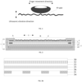
- the working principle of the haptic reproduction device of the pressure film effect is to stick a piezoelectric material on a substrate and apply a high-frequency alternating excitation source. Due to the inverse piezoelectric effect, the piezoelectric material undergoes stretching deformation, which drives the substrate to vibrate and generate specific vibration modes.
- an operator touches a panel with his/her finger as shown in FIG.
- an air gap between the finger and the panel may continuously lift the finger, causing incomplete contact between the finger and the a surface of the substrate, reducing the friction force on the surface of the substrate.
- control on the friction on the surface of the substrate may be achieved, thereby achieving haptic perception effect.
- four sides of the substrate cannot be completely fixed. Because when the substrate is completely fixed, the vibration amplitude of the substrate will be greatly reduced, and the haptic sensation will be significantly reduced. If the substrate is not fixed, a contact surface between a vibrating substrate and a module will generate some noise, which affects the haptic experience.
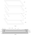
- FIG. 2 is a schematic structural diagram of a display device provided in an embodiment of the present disclosure.
- Embodiment of the present disclosure provides a display device, as shown in FIG. 2 , including:
- the first isolation structure 4 is used to isolate the touch module 3 and the module outer frame 1, maintain a certain distance between the touch module 3 and the module outer frame 1; and the second isolation structure 5 is used to isolate the display module 2 and the touch module 3, maintain a certain distance between the display module 2 and the touch module 3, avoiding high-frequency noise and heat generated by the friction between the touch module 3 and the display module 2 and the friction between the touch module 3 and the module outer frame 1, which affects the user experience.
- first isolation structure 4 and the second isolation structure 5 are not completely fixed to the touch module 3, so the first isolation structure 4 and the second isolation structure 5 will not significantly suppress the vibration of the touch module 3 during the operation of the haptic sensor 31. That is, the intensity of the haptic perception may be effectively ensured without reducing the vibration amplitude of the touch module 3.
- the first isolation structure 4 and the second isolation structure 5 should choose materials with lower Young's modulus, such as materials with Young's modulus less than 0.1 MPa.
- the material of the first isolation structure 4 may be selected from polydimethylsiloxane PDMS, foam or rubber, etc.
- the material of the second isolation structure 5 may be selected as PDMS, foam, or rubber.
- the first isolation structure 4 and the second isolation structure 5 can choose the same material or different materials, which is not limited here.
- the display module 2 can include a display screen 21 and another component 22, and the another component 22 is arranged at a side facing away from a light emitting side of the display screen 21.
- the display screen 21 may be a liquid crystal display screen, the corresponding another component 22 may be a backlight module, etc.
- the display screen 21 may also be an organic light emitting display screen, and the corresponding another component 22 may be a heat dissipation module, etc.
- the specific structure of the display module 2 is not limited here.
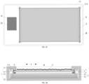
- FIGS. 3A and 3C respectively show schematic structural diagrams of a touch module in a display device provided in embodiments of the present disclosure
- FIGS. 3B and 3D are top view schematic diagrams of a touch module in a display device provided in embodiments of the present disclosure.
- the touch module 3 may include a substrate 30, a touch structure 32, a first insulation layer 33, a haptic sensor 31, and a flat layer 34 (or the flat layer 34 may not be set), where the touch structure 32, the first insulation layer 33, the haptic sensor 31, and the flat layer 34 are sequentially arranged on a side of the substrate 30 facing the display module 2 in stack.
- the touch structure 32 may adopt a single-layer or multi-layer structure.
- the touch structure 32 may adopt a capacitive touch structure, composed of patterned ITO or nano metal wiring.
- the specific composition of the touch structure 32 is not limited here.
- the first insulation layer 33 is configured to protect the touch structure 32, and the first insulation layer 33 may be formed by an inorganic material, such as SiNx or SiOz, or an organic material, such as PI.
- the touch module 3 includes a shielding conductive layer 35 arranged between the first insulation layer 33 and the haptic sensor 31, and a second insulation layer 36 arranged between the shielding conductive layer 35 and the haptic sensor 31.
- the shielding conductive layer 35 may be an ITO covering layer of an entire surface.
- the shielding conductive layer 35 is configured to isolate piezoelectric vibration signals and touch screen signals, avoiding cross talk.
- the shielding conductive layer 35 is generally connected to the system grounding (GND) signal.
- the second insulation layer 36 is configured to protect the shielding conductive layer 35, and the second insulation layer 36 may be formed by an inorganic material, such as SiNx or SiO 2 , or an organic material, such as PI.
- a standing wave is generated on a surface of the touch module 3 facing away from the display module 2.
- the standing wave vibrates along the x-axis or y-axis parallel to the surface of touch module 3, and has certain amplitude in a direction perpendicular to the surface of the touch module 3.
- a gap between the touch module 3 and the display module 2 should be greater than the amplitude of the standing wave.
- the maximum amplitude generated by the standing wave is within 2 um, so the gap between the touch module 3 and the display module 2 generally needs to be greater than 2 um.
- Embodiment 1 is as follows.
- the module outer frame 1 includes a module side frame 13, a module bottom frame 12, and a module top frame 11, and the module top frame 11 includes a display opening window B.
- the module top frame 11, module bottom frame 12, and module side frame 13 form an accommodating space A, and the display module 2, the touch module 3, the first isolation structure 4, and the second isolation structure 5 are all arranged in the accommodating space A.
- the module side frame 13 can form an integral structure with the module bottom frame 12; the module side frame 13 can form an integral structure with the module top frame 11; or, as shown in FIG. 2 , a part of the module side frame 13 form an integral structure with the module bottom frame 12, and another part of the module side frame 13 form an integral structure with the module top frame 11, which is not limited here.
- the display module 2, the second isolation structure 5, the touch module 3, and the first isolation structure 4 may be sequentially assembled on the module bottom frame 12, and finally the module top frame 11 may be installed to form a complete display device.
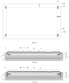
- FIG. 4 is an exploded view corresponding to the display device structure shown in FIG. 2
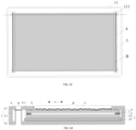
- FIG. 5 is an upward view of the display device structure viewed from one side of the module bottom frame shown in FIG. 2 , and only part of the components of the display device are shown.
- FIG. 2 may be considered as a cross-sectional view of the dashed line in FIG. 5 .
- the first isolation structure 4 may be located at positions of two opposite edge frames of the touch module 3, and the second isolation structure 5 may be located at positions of two opposite edge frames of the display module 2. Moreover, the first isolation structure 4 and the second isolation structure 5 are generally arranged at positions of edge frames on same sides.
- an extension direction of each of the two opposite edge frames where the first isolation structure 4 and the second isolation structure 5 are located is perpendicular to a vibration propagation direction t of the standing wave C.
- the two frames where the first isolation structure 4 and the second isolation structure 5 are located may be short edge frames, that is, there is no isolation structure fixed with the touch module 3 at long edge frames.
- the haptic sensor 31 should be covered by the module top frame 11 and not overlapped with the display opening window B in order to avoid impact of the haptic sensor 31 on display.
- the haptic sensor 31, the first isolation structure 4, and the second isolation structure 5 may be simultaneously located at positions of two opposite short edge frames. As shown in FIG.
- a relationship between a width L2 of the haptic sensor 31 at one short edge frame and a distance L1 between the haptic sensor 31 and an edge of the short edge frame satisfies: 0 ⁇ L1 ⁇ L/n; and 0 ⁇ L2 ⁇ L/n; where n is a positive integer, a value of n may be 5 ⁇ n ⁇ 100, and L is a length of the touch module, a value of L may be 50 mm ⁇ L ⁇ 500 mm, and a value of L2 may be about twice the value of L1.
- a distance L3 between the haptic sensor 31 and the display opening window B is larger than or equal to 0, and a distance L4 between the haptic sensor 31 and an edge of the long edge frame is larger than or equal to 0.
- a distance M between the display opening window B and the edge of the short edge frame is larger than or equal to a sum of L1, L2 and L3.
- a distance N between the display opening window B and the edge of the long edge frame is larger than or equal to 0.
- a size of display opening window B is generally smaller than a size of touch module 3 and a size of display module 2.
- the first isolation structure 4 and the second isolation structure 5 are covered by the module top frame 11, and an orthogonal projection of the first isolation structure 4 and an orthogonal projection of the second isolation structure 5 on the module bottom frame 12 do not overlap with the display opening window B.
- the first isolation structure 4 may be fixed on a surface of the touch module 3 facing the module top frame 11.
- the first isolation structure 4 is arranged in a peripheral area of the display opening window B to isolate the touch module 3 and the module top frame 11 without affecting the display.
- An edge of the first isolation structure 4 on a surface of the touch module 3 facing the module top frame 11 may extend beyond the touch module 3, or may be within a range of the touch module 3, which is not limited here.
- a shape of the first isolation structure 4 may be roughly a strip.
- FIG. 6 is another schematic structural diagram of a display device provided in an embodiment of the present disclosure.
- the first isolation structure 4 may be fixed on a side face of the touch module 3 facing the module side frame 13, that is, the first isolation structure 4 extends from a surface of the touch module 3 facing the module top frame 11 to the side face of the touch module 3 after bending.
- the present disclosure there is no clear limit on the length of the portion of the first isolation structure 4 extending to the side face of the touch module 3.
- the length of the portion of the first isolation structure 4 extending to the side face of the touch module 3 may be approximately same as a thickness of the touch module 3. As shown in FIG. 8 , a cross-sectional shape of the first isolation structure 4 may be roughly an L-shaped strip.
- the second isolation structure 5 may be fixed on the surface of display module 2 facing touch module 3.
- the second isolation structure 5 may be fixed at edge frames of a non-display area on both sides of a display surface of the display module 2.
- An edge of the second isolation structure 5 on a surface of the display module 2 facing the touch module 3 may extend beyond the display module 2, or may be within a range of the display module 2, which is not limited here.
- a shape of the second isolation structure 5 may be roughly a strip.
- FIG. 7 is another schematic structural diagram of a display device provided in an embodiment of the present disclosure.
- Fig. 8 is an exploded view corresponding to the display device structure shown in FIG. 7 .
- the second isolation structure 5 may be fixed on a side face of the display module 2 facing the module side frame 13, that is, the second isolation structure 5 extends from a surface of the display module 2 facing the touch module 3 to the side face of the display module 2 after bending.
- the length of the portion of the second isolation structure 5 extending to the side face of the display module 2 may be approximately same as a thickness of the display screen 21 in the display module 2.
- a cross-sectional shape of the second isolation structure 5 may be roughly an L-shaped strip.
- Embodiment 2 is follows.
- FIGS. 9 to 12 are another schematic structural diagram of a display device provided in embodiments of the present disclosure.
- FIG. 13 is an upward view of the display device structure viewed from one side of the module bottom frame shown in FIGS. 9 to 12 , and only part of components of the display device are shown.
- FIGS. 9 to 12 may be considered as a cross-sectional view of the dashed line in FIG. 13 .
- a limiting structure 111 may be arranged on a side of the module top frame 11 facing the module bottom frame 12, and the limiting structure 111 is configured to limit a position of the touch module 3.
- FIG. 13 only illustrates a specific implementation of a limiting structure 111, and the present disclosure does not limit the specific structure of the limiting structure 111.
- the first isolation structure 4 may be fixed on a surface of the touch module 3 facing the module top frame 11. That is, the first isolation structure 4 is arranged in a peripheral area of the display opening window B to isolate the touch module 3 and the module top frame 11 without affecting the display. An edge of the first isolation structure 4 on a surface of the touch module 3 facing the module top frame 11 may extend beyond the touch module 3, or may be within the range of the touch module 3, which is not limited here.
- a shape of the first isolation structure 4 may be roughly a strip.
- the first isolation structure 4 may be fixed between the touch module 3 and the limiting structure 111. That is, the first isolation structure 4 extends from a surface of the touch module 3 facing the module top frame 11 to a side face of the touch module 3 after bending. Moreover, in the present disclosure, there is no clear limit on the length of the portion of the first isolation structure 4 extending to the side face of the touch module 3. The length of the portion of the first isolation structure 4 extending to the side face of the touch module 3 may be approximately same as a thickness of the touch module 3. In some embodiments, a cross-sectional shape of the first isolation structure 4 may be roughly an L-shaped strip.
- FIG. 14 is another schematic structural diagram of a display device provided in embodiments of the present disclosure.
- FIG. 15 is an upward view of the display device structure viewed from one side of the module bottom frame shown in FIG. 14 , and only part of components of the display device are shown.
- a display sample 6 may be arranged according to client requirements.
- a corresponding display opening window D may be arranged in the module top frame 11, a the size of the display opening window D should be smaller than a size of the display sample 6.
- Positions of display opening window D and display opening window B at the module top frame 11 may be arranged according to client requirements, and will not be elaborated here.
- the structure of the second isolation structure 5 in Embodiment 2 is the same as the structure of the second isolation structure 5 in Embodiment 1, and will not be elaborated here.
- Embodiment 3 is as follows.
- Fig. 16 is another schematic structural diagram of a display device provided in embodiments of the present disclosure.
- the module outer frame 1 may further include a fixing component 14 located in the accommodation space A, and the fixing component 14 is configured to fix the display module 2 and the touch module 3.
- One end of the fixing component 14 may be fixed with the module top frame 11, and the other end of the fixing component 14 may be fixed with the module bottom frame 12.
- the specific structure of the fixing component 14 is not limited in the present disclosure.
- the first isolation structure 4 may be arranged between the fixing component 14 and the touch module 3. Moreover, the first isolation structure 4 is arranged in ta peripheral area of the display opening window B to isolate the touch module 3, the fixing component 14 and the module top frame 11 without affecting the display.
- the structure of the second isolation structure 5 in Embodiment 3 is the same as the structure of the second isolation structure 5 in Embodiment 1, and will not be elaborated here.
- Embodiment 4 is as follows.
- FIG. 17 is an upward view of a display device viewed from one side of the module bottom frame provided in an embodiment, only illustrating the module top frame 11 and the first isolation structure 4.
- the shape of the first isolation structure 4 is a discontinuous pattern. That is, the first isolation structure 4 located on one edge frame includes a plurality of first isolation parts 41 arranged at intervals. In FIG. 17 , only one pattern of the first isolation unit 41 is illustrated.
- the structure of the first isolation part 41 is the same as the first isolation structure in Embodiment 1, Embodiment 2 or Embodiment 3, and will not be elaborated here.
- the shape of the second isolation structure 5 is a discontinuous pattern. That is, the second isolation structure 5 located on one edge frame includes a plurality of second isolation parts arranged at intervals.
- the structure of the second isolation part is the same as the second isolation structure in Embodiment 1, Embodiment 2 or Embodiment 3, and will not be elaborated here.
- Embodiment 5 is as follows.
- FIGS. 18 and 19 are other schematic structural diagrams of a display device provided in embodiments of the present disclosure.
- the module outer frame 1 can include the module side frame 13 and the module bottom frame 12. That is, the module outer frame 1 is not provided with a module top cover, and the display opening window B is arranged at a side away from the module bottom frame 12.
- An accommodating space A is formed by the module bottom frame 12 and the module side frame 13.
- the display module 2, the touch module 3, the first isolation structure 4, and the second isolation structure 5 are all arranged in the accommodating space A.
- the module side frame 13 can form an integral structure with the module bottom frame 12.
- a complete display device may be formed by sequentially assembling the display module 2, the second isolation structure 5, the touch module 3, and the first isolation structure 4 on the module bottom frame 12.
- the first isolation structure 4 may be arranged between the module side frame 13 and the touch module 3. Moreover, in order to fix the position of the touch module 3, the first isolation structure 4 needs to be arranged around the touch module 3, that is, the first isolation structure 4 is arranged at four edge frames of the touch module 3. Moreover, as shown in FIGS. 18 and 19 , the top of module side frame 13 may be flush with the first isolation structure 4 and the touch module 3.
- the touch module 3 can include a light-blocking layer 37 that blocks the haptic sensor 31 and the second isolation structure 5.
- the middle area of the light-blocking layer 37 is a transparent area, and the distance a between a light-blocking area in the light-blocking layer 37 and the edge of the short edge frame is greater than or equal to the sum of L1, L2 and L3.
- the distance b between the light-blocking area in the shading layer 37 and the edge of the long edge frame is greater than or equal to 0.
- the structure of the second isolation structure 5 in Embodiment 5 is the same as the structure of the second isolation structure 5 in Embodiment 1, Embodiment 2, Embodiment 3 or Embodiment 4, and will not be elaborated here.
- the first isolation structure 4 is used to isolate the touch module 3 and module outer frame 1, maintain a certain distance between the touch module 3 and the module outer frame 1; and the second isolation structure 5 is used to isolate the display module 2 and the touch module 3, maintain a certain distance between the display module 2 and the touch module 3, avoiding high-frequency noise and heat generated by friction between the touch module 3 and the display module 2 and friction between the touch module 3 and the module outer frame 1, which affects the user experience.
- first isolation structure 4 and the second isolation structure 5 are not completely fixed to the touch module 3, so the first isolation structure 4 and the second isolation structure 5 may not significantly suppress the vibration of the touch module 3 during the operation of the haptic sensor 31. That is, the intensity of haptic perception can be effectively ensured without reducing the vibration amplitude of touch module 3.
Landscapes
- Engineering & Computer Science (AREA)
- Theoretical Computer Science (AREA)
- Computer Hardware Design (AREA)
- General Engineering & Computer Science (AREA)
- Human Computer Interaction (AREA)
- Physics & Mathematics (AREA)
- General Physics & Mathematics (AREA)
- Microelectronics & Electronic Packaging (AREA)
- Devices For Indicating Variable Information By Combining Individual Elements (AREA)
Applications Claiming Priority (2)
| Application Number | Priority Date | Filing Date | Title |
|---|---|---|---|
| CN202110818073.1A CN115639918B (zh) | 2021-07-20 | 显示装置 | |
| PCT/CN2022/103398 WO2023000959A1 (zh) | 2021-07-20 | 2022-07-01 | 显示装置 |
Publications (3)
| Publication Number | Publication Date |
|---|---|
| EP4339749A1 true EP4339749A1 (de) | 2024-03-20 |
| EP4339749A4 EP4339749A4 (de) | 2024-10-09 |
| EP4339749B1 EP4339749B1 (de) | 2025-11-26 |
Family
ID=84940145
Family Applications (1)
| Application Number | Title | Priority Date | Filing Date |
|---|---|---|---|
| EP22845124.1A Active EP4339749B1 (de) | 2021-07-20 | 2022-07-01 | Anzeigevorrichtung |
Country Status (3)
| Country | Link |
|---|---|
| US (1) | US12426171B2 (de) |
| EP (1) | EP4339749B1 (de) |
| WO (1) | WO2023000959A1 (de) |
Family Cites Families (23)
| Publication number | Priority date | Publication date | Assignee | Title |
|---|---|---|---|---|
| KR101054111B1 (ko) | 2006-02-09 | 2011-08-03 | 니혼샤신 인사츠 가부시키가이샤 | 보호패널을 부착한 전자기기 |
| JP2010072471A (ja) * | 2008-09-19 | 2010-04-02 | Three M Innovative Properties Co | 透明粘着シート、それを含む画像表示装置及び、その画像表示装置の作製方法 |
| TWI631538B (zh) | 2009-01-28 | 2018-08-01 | 日商半導體能源研究所股份有限公司 | 顯示裝置 |
| JP5623754B2 (ja) | 2010-02-04 | 2014-11-12 | 株式会社ジャパンディスプレイ | 表示装置およびその製造方法 |
| JP5630119B2 (ja) * | 2010-07-26 | 2014-11-26 | 株式会社リコー | タッチパネル装置、これを含むタッチパネル付き表示装置、及びタッチパネル装置の制御方法 |
| JP5693606B2 (ja) * | 2010-11-12 | 2015-04-01 | 京セラ株式会社 | 電子機器、およびこれを備えた携帯端末 |
| JP5665591B2 (ja) | 2011-02-18 | 2015-02-04 | 京セラ株式会社 | 電子機器 |
| US8666456B2 (en) * | 2011-10-12 | 2014-03-04 | Htc Corporation | Handheld electronic apparatus |
| US20130335377A1 (en) * | 2012-06-15 | 2013-12-19 | Tzyy-Pyng Lin | Notebook touch input device |
| JP6264287B2 (ja) * | 2012-08-31 | 2018-01-24 | 日本電気株式会社 | 触力覚提示装置、情報端末、触力覚提示方法、およびプログラム |
| JP5347096B1 (ja) * | 2012-09-13 | 2013-11-20 | 株式会社ワンダーフューチャーコーポレーション | タッチパネルの製造方法及びタッチパネル、並びにタッチパネルと表示装置を具備する入出力一体型装置 |
| JP6026548B2 (ja) * | 2012-09-24 | 2016-11-16 | 京セラ株式会社 | 振動装置、および電子機器 |
| JP5909682B2 (ja) * | 2012-10-09 | 2016-04-27 | パナソニックIpマネジメント株式会社 | 電子機器 |
| TWI489118B (zh) * | 2013-06-11 | 2015-06-21 | Au Optronics Corp | 觸控面板及觸控顯示面板的製造方法 |
| MX338463B (es) * | 2013-09-26 | 2016-04-15 | Fujitsu Ltd | Aparato de control de accionador, dispositivo electronico y metodo de control del accionador. |
| JP6555608B2 (ja) | 2014-12-01 | 2019-08-07 | Tianma Japan株式会社 | ディスプレイ装置および電子機器 |
| CN104679241B (zh) | 2015-01-30 | 2018-02-06 | 南京航空航天大学 | 一种宽幅摩擦力控制触觉再现装置及方法 |
| JP6818572B2 (ja) | 2017-01-31 | 2021-01-20 | 京セラ株式会社 | タッチパネルおよび表示装置 |
| US10768702B2 (en) * | 2017-03-28 | 2020-09-08 | Kyocera Corporation | Display device |
| JP2019012408A (ja) * | 2017-06-30 | 2019-01-24 | 日本電産サンキョー株式会社 | 入力装置 |
| KR102564250B1 (ko) * | 2018-09-11 | 2023-08-07 | 삼성디스플레이 주식회사 | 표시 장치 |
| WO2020241513A1 (ja) * | 2019-05-28 | 2020-12-03 | 日本精機株式会社 | 車両用表示装置 |
| JP7835536B2 (ja) * | 2021-05-07 | 2026-03-25 | コニカミノルタ株式会社 | 操作入力装置および画像形成装置 |
-
2022
- 2022-07-01 EP EP22845124.1A patent/EP4339749B1/de active Active
- 2022-07-01 WO PCT/CN2022/103398 patent/WO2023000959A1/zh not_active Ceased
- 2022-07-01 US US18/579,942 patent/US12426171B2/en active Active
Also Published As
| Publication number | Publication date |
|---|---|
| EP4339749B1 (de) | 2025-11-26 |
| US20240244768A1 (en) | 2024-07-18 |
| US12426171B2 (en) | 2025-09-23 |
| WO2023000959A1 (zh) | 2023-01-26 |
| CN115639918A (zh) | 2023-01-24 |
| EP4339749A4 (de) | 2024-10-09 |
Similar Documents
| Publication | Publication Date | Title |
|---|---|---|
| US9785239B2 (en) | Display device and electronic apparatus | |
| KR102463757B1 (ko) | 접촉 감응 소자, 이를 포함하는 표시 장치 및 표시 장치의 제조 방법 | |
| CN100426205C (zh) | 具有低外形衍射栅转换器组件的声触摸传感器 | |
| KR101635297B1 (ko) | 전자 기기 | |
| JP6103141B2 (ja) | 振動装置 | |
| CN107533408B (zh) | 电子设备 | |
| KR101177610B1 (ko) | 터치스크린장치 | |
| CN102004571B (zh) | 触摸屏装置 | |
| TW201135689A (en) | Display panel | |
| US20120139850A1 (en) | Haptic driving assembly and electronic device using the same | |
| CN103970338B (zh) | 触摸面板支撑体 | |
| WO2014046279A1 (ja) | 振動装置、および電子機器 | |
| JP5848189B2 (ja) | 入力機能付き表示装置、および電子機器 | |
| JP6133619B2 (ja) | 振動装置、電子機器、および携帯端末 | |
| KR101095128B1 (ko) | 터치스크린 장치 | |
| EP4339749A1 (de) | Anzeigevorrichtung | |
| CN102859472B (zh) | 电子设备以及具备该电子设备的便携式终端 | |
| JP6001482B2 (ja) | 入力装置および電子機器 | |
| CN115639918B (zh) | 显示装置 | |
| JP2012043362A (ja) | 入力機能付き表示装置 | |
| JPWO2019093233A1 (ja) | タッチセンサ | |
| TWI622916B (zh) | 觸控顯示裝置及其操作方法 | |
| US12487680B2 (en) | Haptic feedback panel, haptic feedback method therefor, and haptic feedback device therefor | |
| JP6147491B2 (ja) | 電子機器及び組立方法 | |
| JP2006343921A (ja) | タッチパネルの製造方法及び電気光学装置の製造方法 |
Legal Events
| Date | Code | Title | Description |
|---|---|---|---|
| STAA | Information on the status of an ep patent application or granted ep patent |
Free format text: STATUS: THE INTERNATIONAL PUBLICATION HAS BEEN MADE |
|
| PUAI | Public reference made under article 153(3) epc to a published international application that has entered the european phase |
Free format text: ORIGINAL CODE: 0009012 |
|
| STAA | Information on the status of an ep patent application or granted ep patent |
Free format text: STATUS: REQUEST FOR EXAMINATION WAS MADE |
|
| 17P | Request for examination filed |
Effective date: 20231215 |
|
| AK | Designated contracting states |
Kind code of ref document: A1 Designated state(s): AL AT BE BG CH CY CZ DE DK EE ES FI FR GB GR HR HU IE IS IT LI LT LU LV MC MK MT NL NO PL PT RO RS SE SI SK SM TR |
|
| REG | Reference to a national code |
Ref country code: DE Ref legal event code: R079 Free format text: PREVIOUS MAIN CLASS: G06F0003041000 Ipc: G06F0001160000 Ref country code: DE Ref legal event code: R079 Ref document number: 602022025820 Country of ref document: DE Free format text: PREVIOUS MAIN CLASS: G06F0003041000 Ipc: G06F0001160000 |
|
| A4 | Supplementary search report drawn up and despatched |
Effective date: 20240911 |
|
| RIC1 | Information provided on ipc code assigned before grant |
Ipc: G06F 3/041 20060101ALN20240905BHEP Ipc: G06F 3/01 20060101ALI20240905BHEP Ipc: G06F 1/16 20060101AFI20240905BHEP |
|
| DAV | Request for validation of the european patent (deleted) | ||
| DAX | Request for extension of the european patent (deleted) | ||
| GRAP | Despatch of communication of intention to grant a patent |
Free format text: ORIGINAL CODE: EPIDOSNIGR1 |
|
| STAA | Information on the status of an ep patent application or granted ep patent |
Free format text: STATUS: GRANT OF PATENT IS INTENDED |
|
| RIC1 | Information provided on ipc code assigned before grant |
Ipc: G06F 1/16 20060101AFI20250613BHEP Ipc: G06F 3/01 20060101ALI20250613BHEP Ipc: G06F 3/041 20060101ALN20250613BHEP |
|
| INTG | Intention to grant announced |
Effective date: 20250709 |
|
| GRAS | Grant fee paid |
Free format text: ORIGINAL CODE: EPIDOSNIGR3 |
|
| GRAA | (expected) grant |
Free format text: ORIGINAL CODE: 0009210 |
|
| STAA | Information on the status of an ep patent application or granted ep patent |
Free format text: STATUS: THE PATENT HAS BEEN GRANTED |
|
| AK | Designated contracting states |
Kind code of ref document: B1 Designated state(s): AL AT BE BG CH CY CZ DE DK EE ES FI FR GB GR HR HU IE IS IT LI LT LU LV MC MK MT NL NO PL PT RO RS SE SI SK SM TR |
|
| REG | Reference to a national code |
Ref country code: CH Ref legal event code: F10 Free format text: ST27 STATUS EVENT CODE: U-0-0-F10-F00 (AS PROVIDED BY THE NATIONAL OFFICE) Effective date: 20251126 Ref country code: GB Ref legal event code: FG4D |
|
| REG | Reference to a national code |
Ref country code: IE Ref legal event code: FG4D |
|
| REG | Reference to a national code |
Ref country code: DE Ref legal event code: R096 Ref document number: 602022025820 Country of ref document: DE |
|
| REG | Reference to a national code |
Ref country code: NL Ref legal event code: MP Effective date: 20251126 |
|
| PG25 | Lapsed in a contracting state [announced via postgrant information from national office to epo] |
Ref country code: ES Free format text: LAPSE BECAUSE OF FAILURE TO SUBMIT A TRANSLATION OF THE DESCRIPTION OR TO PAY THE FEE WITHIN THE PRESCRIBED TIME-LIMIT Effective date: 20251126 |
|
| REG | Reference to a national code |
Ref country code: LT Ref legal event code: MG9D |
|
| PG25 | Lapsed in a contracting state [announced via postgrant information from national office to epo] |
Ref country code: NO Free format text: LAPSE BECAUSE OF FAILURE TO SUBMIT A TRANSLATION OF THE DESCRIPTION OR TO PAY THE FEE WITHIN THE PRESCRIBED TIME-LIMIT Effective date: 20260226 |
|
| PG25 | Lapsed in a contracting state [announced via postgrant information from national office to epo] |
Ref country code: FI Free format text: LAPSE BECAUSE OF FAILURE TO SUBMIT A TRANSLATION OF THE DESCRIPTION OR TO PAY THE FEE WITHIN THE PRESCRIBED TIME-LIMIT Effective date: 20251126 Ref country code: AT Free format text: LAPSE BECAUSE OF FAILURE TO SUBMIT A TRANSLATION OF THE DESCRIPTION OR TO PAY THE FEE WITHIN THE PRESCRIBED TIME-LIMIT Effective date: 20251126 Ref country code: HR Free format text: LAPSE BECAUSE OF FAILURE TO SUBMIT A TRANSLATION OF THE DESCRIPTION OR TO PAY THE FEE WITHIN THE PRESCRIBED TIME-LIMIT Effective date: 20251126 |
|
| REG | Reference to a national code |
Ref country code: AT Ref legal event code: MK05 Ref document number: 1861690 Country of ref document: AT Kind code of ref document: T Effective date: 20251126 |
|
| PG25 | Lapsed in a contracting state [announced via postgrant information from national office to epo] |
Ref country code: NL Free format text: LAPSE BECAUSE OF FAILURE TO SUBMIT A TRANSLATION OF THE DESCRIPTION OR TO PAY THE FEE WITHIN THE PRESCRIBED TIME-LIMIT Effective date: 20251126 |
|
| PG25 | Lapsed in a contracting state [announced via postgrant information from national office to epo] |
Ref country code: RS Free format text: LAPSE BECAUSE OF FAILURE TO SUBMIT A TRANSLATION OF THE DESCRIPTION OR TO PAY THE FEE WITHIN THE PRESCRIBED TIME-LIMIT Effective date: 20260226 |
|
| PG25 | Lapsed in a contracting state [announced via postgrant information from national office to epo] |
Ref country code: IS Free format text: LAPSE BECAUSE OF FAILURE TO SUBMIT A TRANSLATION OF THE DESCRIPTION OR TO PAY THE FEE WITHIN THE PRESCRIBED TIME-LIMIT Effective date: 20260326 |
|
| PG25 | Lapsed in a contracting state [announced via postgrant information from national office to epo] |
Ref country code: PT Free format text: LAPSE BECAUSE OF FAILURE TO SUBMIT A TRANSLATION OF THE DESCRIPTION OR TO PAY THE FEE WITHIN THE PRESCRIBED TIME-LIMIT Effective date: 20260326 |
|
| PG25 | Lapsed in a contracting state [announced via postgrant information from national office to epo] |
Ref country code: PL Free format text: LAPSE BECAUSE OF FAILURE TO SUBMIT A TRANSLATION OF THE DESCRIPTION OR TO PAY THE FEE WITHIN THE PRESCRIBED TIME-LIMIT Effective date: 20251126 |
|
| PG25 | Lapsed in a contracting state [announced via postgrant information from national office to epo] |
Ref country code: LV Free format text: LAPSE BECAUSE OF FAILURE TO SUBMIT A TRANSLATION OF THE DESCRIPTION OR TO PAY THE FEE WITHIN THE PRESCRIBED TIME-LIMIT Effective date: 20251126 |