EP4339929A1 - Anzeigesubstrat und ansteuerungsverfahren dafür sowie anzeigevorrichtung - Google Patents
Anzeigesubstrat und ansteuerungsverfahren dafür sowie anzeigevorrichtung Download PDFInfo
- Publication number
- EP4339929A1 EP4339929A1 EP21965272.4A EP21965272A EP4339929A1 EP 4339929 A1 EP4339929 A1 EP 4339929A1 EP 21965272 A EP21965272 A EP 21965272A EP 4339929 A1 EP4339929 A1 EP 4339929A1
- Authority
- EP
- European Patent Office
- Prior art keywords
- transistor
- column
- sub
- pixels
- electrically connected
- Prior art date
- Legal status (The legal status is an assumption and is not a legal conclusion. Google has not performed a legal analysis and makes no representation as to the accuracy of the status listed.)
- Pending
Links
- 239000000758 substrate Substances 0.000 title claims abstract description 91
- 238000000034 method Methods 0.000 title claims abstract description 16
- 238000005192 partition Methods 0.000 claims description 372
- 238000010586 diagram Methods 0.000 description 17
- 238000005516 engineering process Methods 0.000 description 5
- 238000004088 simulation Methods 0.000 description 4
- 238000012986 modification Methods 0.000 description 3
- 230000004048 modification Effects 0.000 description 3
- 230000008569 process Effects 0.000 description 3
- 230000009286 beneficial effect Effects 0.000 description 2
- 239000003086 colorant Substances 0.000 description 2
- 229910021417 amorphous silicon Inorganic materials 0.000 description 1
- 230000005540 biological transmission Effects 0.000 description 1
- 230000008859 change Effects 0.000 description 1
- 230000005669 field effect Effects 0.000 description 1
- 230000006870 function Effects 0.000 description 1
- 230000008447 perception Effects 0.000 description 1
- 229910021420 polycrystalline silicon Inorganic materials 0.000 description 1
- 229920005591 polysilicon Polymers 0.000 description 1
- 239000002699 waste material Substances 0.000 description 1
Images






Classifications
-
- G—PHYSICS
- G09—EDUCATION; CRYPTOGRAPHY; DISPLAY; ADVERTISING; SEALS
- G09G—ARRANGEMENTS OR CIRCUITS FOR CONTROL OF INDICATING DEVICES USING STATIC MEANS TO PRESENT VARIABLE INFORMATION
- G09G3/00—Control arrangements or circuits, of interest only in connection with visual indicators other than cathode-ray tubes
- G09G3/001—Control arrangements or circuits, of interest only in connection with visual indicators other than cathode-ray tubes using specific devices not provided for in groups G09G3/02 - G09G3/36, e.g. using an intermediate record carrier such as a film slide; Projection systems; Display of non-alphanumerical information, solely or in combination with alphanumerical information, e.g. digital display on projected diapositive as background
- G09G3/003—Control arrangements or circuits, of interest only in connection with visual indicators other than cathode-ray tubes using specific devices not provided for in groups G09G3/02 - G09G3/36, e.g. using an intermediate record carrier such as a film slide; Projection systems; Display of non-alphanumerical information, solely or in combination with alphanumerical information, e.g. digital display on projected diapositive as background to produce spatial visual effects
-
- G—PHYSICS
- G09—EDUCATION; CRYPTOGRAPHY; DISPLAY; ADVERTISING; SEALS
- G09G—ARRANGEMENTS OR CIRCUITS FOR CONTROL OF INDICATING DEVICES USING STATIC MEANS TO PRESENT VARIABLE INFORMATION
- G09G3/00—Control arrangements or circuits, of interest only in connection with visual indicators other than cathode-ray tubes
- G09G3/20—Control arrangements or circuits, of interest only in connection with visual indicators other than cathode-ray tubes for presentation of an assembly of a number of characters, e.g. a page, by composing the assembly by combination of individual elements arranged in a matrix no fixed position being assigned to or needed to be assigned to the individual characters or partial characters
- G09G3/2007—Display of intermediate tones
- G09G3/2074—Display of intermediate tones using sub-pixels
-
- H—ELECTRICITY
- H10—SEMICONDUCTOR DEVICES; ELECTRIC SOLID-STATE DEVICES NOT OTHERWISE PROVIDED FOR
- H10D—INORGANIC ELECTRIC SEMICONDUCTOR DEVICES
- H10D86/00—Integrated devices formed in or on insulating or conducting substrates, e.g. formed in silicon-on-insulator [SOI] substrates or on stainless steel or glass substrates
- H10D86/40—Integrated devices formed in or on insulating or conducting substrates, e.g. formed in silicon-on-insulator [SOI] substrates or on stainless steel or glass substrates characterised by multiple TFTs
-
- G—PHYSICS
- G09—EDUCATION; CRYPTOGRAPHY; DISPLAY; ADVERTISING; SEALS
- G09G—ARRANGEMENTS OR CIRCUITS FOR CONTROL OF INDICATING DEVICES USING STATIC MEANS TO PRESENT VARIABLE INFORMATION
- G09G2300/00—Aspects of the constitution of display devices
- G09G2300/04—Structural and physical details of display devices
- G09G2300/0421—Structural details of the set of electrodes
- G09G2300/0426—Layout of electrodes and connections
-
- G—PHYSICS
- G09—EDUCATION; CRYPTOGRAPHY; DISPLAY; ADVERTISING; SEALS
- G09G—ARRANGEMENTS OR CIRCUITS FOR CONTROL OF INDICATING DEVICES USING STATIC MEANS TO PRESENT VARIABLE INFORMATION
- G09G2310/00—Command of the display device
- G09G2310/02—Addressing, scanning or driving the display screen or processing steps related thereto
- G09G2310/0264—Details of driving circuits
- G09G2310/0275—Details of drivers for data electrodes, other than drivers for liquid crystal, plasma or OLED displays, not related to handling digital grey scale data or to communication of data to the pixels by means of a current
-
- G—PHYSICS
- G09—EDUCATION; CRYPTOGRAPHY; DISPLAY; ADVERTISING; SEALS
- G09G—ARRANGEMENTS OR CIRCUITS FOR CONTROL OF INDICATING DEVICES USING STATIC MEANS TO PRESENT VARIABLE INFORMATION
- G09G2310/00—Command of the display device
- G09G2310/02—Addressing, scanning or driving the display screen or processing steps related thereto
- G09G2310/0264—Details of driving circuits
- G09G2310/0291—Details of output amplifiers or buffers arranged for use in a driving circuit
-
- G—PHYSICS
- G09—EDUCATION; CRYPTOGRAPHY; DISPLAY; ADVERTISING; SEALS
- G09G—ARRANGEMENTS OR CIRCUITS FOR CONTROL OF INDICATING DEVICES USING STATIC MEANS TO PRESENT VARIABLE INFORMATION
- G09G2310/00—Command of the display device
- G09G2310/02—Addressing, scanning or driving the display screen or processing steps related thereto
- G09G2310/0264—Details of driving circuits
- G09G2310/0297—Special arrangements with multiplexing or demultiplexing of display data in the drivers for data electrodes, in a pre-processing circuitry delivering display data to said drivers or in the matrix panel, e.g. multiplexing plural data signals to one D/A converter or demultiplexing the D/A converter output to multiple columns
-
- H—ELECTRICITY
- H10—SEMICONDUCTOR DEVICES; ELECTRIC SOLID-STATE DEVICES NOT OTHERWISE PROVIDED FOR
- H10K—ORGANIC ELECTRIC SOLID-STATE DEVICES
- H10K59/00—Integrated devices, or assemblies of multiple devices, comprising at least one organic light-emitting element covered by group H10K50/00
- H10K59/10—OLED displays
- H10K59/12—Active-matrix OLED [AMOLED] displays
- H10K59/131—Interconnections, e.g. wiring lines or terminals
Definitions
- the present disclosure relates to the field of display technology, and in particular to a display substrate, a driving method therefor, and a display apparatus.
- Naked-eye three-dimensional (3D) technology refers to a 3D display technology with which spatial and depth perception can be achieved without any auxiliary equipment. As users have higher and higher requirements for viewing experience, naked-eye 3D display technology is gradually being applied to display screens.
- Detailed implementations for a display substrate, a driving method therefor and a display device provided by some embodiments of the disclosure are as following.
- some embodiments of the present disclosure provide a display substrate, including:
- each of the reusing circuits includes a first sub-reusing circuit, and the sub-pixels electrically connected to each first sub-reusing circuit are located in at least two of the partitions.
- each of the first sub-reusing circuits is connected among two operational amplifiers and the data lines to which the two operational amplifiers are electrically connected, and the sub-pixels electrically connected to each of the first sub-reusing circuits are in two of the partitions.
- n is a positive integer
- each of the partitions includes i columns of pixel islands, where i is an integer greater than or equal to 2; the sub-pixels electrically connected to each of the first sub-reusing circuits are located in a j th column of pixel island in the m th partition and the j th column of pixel island in the (m+n) th partition, j is an integer greater than or equal to 1 and less than or equal to i.
- each of the pixel islands includes k sub-pixels arranged in a single row, where k is an even number; the sub-pixels electrically connected to each of the first sub-reusing circuits are at least part of the sub-pixels in a h th column of a j th column of the pixel island in a m th partition, and at least part of the sub-pixels in the h th column of the j th column of the pixel island in a (m+n) th partition, wherein h is an integer greater than or equal to 1 and less than or equal to k.
- one of the data lines is connected between one of the operational amplifiers and one column of the sub-pixels.
- the sub-pixels electrically connected to each of the first sub-reusing circuits are the sub-pixels in the h th column of the j th column of the pixel island in the m th partition, and the sub-pixels in the h th column of the j th column of the pixel island in the (m+n) th partition.
- each of the reusing circuit further includes a second sub-reusing circuit; each second sub-reusing circuit is connected between two columns of sub-pixels in a same column of the pixel island and two first sub-reusing circuits corresponding to the two columns of sub-pixels.
- k is a multiple of 4
- h is an integer greater than or equal to 1 and less than or equal to k/4, and an integer greater than or equal to (1+k/4) and less than or equal to (k-4);
- each of the second sub-reusing circuits is electrically connected to the sub-pixels in the h th column and the (h+k/4) th column of the same column of pixel island, respectively.
- each of the first sub-reusing circuits which is connected to the h th column of sub-pixels in the j th column of pixel island in the m th partition and the h th column of sub-pixels in the j th column of pixel island in the (m+n) th partition, includes a first transistor, a second transistor and a third transistor;
- two data lines are connected between one operational amplifier and one column of sub-pixels, and one of the two data lines is connected to odd-numbered rows of sub-pixels in the one column, the other one of the two data lines is connected to even-numbered rows of sub-pixels in the one column.
- sub-pixels electrically connected to each of the first sub-reusing circuits are even-numbered rows of sub-pixels in the h th column of the j th column of pixel island in the m th partition, and even-numbered rows of sub-pixels in the h th of the j th column of pixel island in the (m+n) th partition.
- each of the first sub-reusing circuits includes: a thirteenth transistor and a fourteenth transistor;
- the display substrate provided by the present disclosure further including a plurality of gating circuits in the frame area; each of the plurality of gating circuits is connected among one operational amplifier and two data lines corresponding to the one operational amplifier.
- each of the plurality of gating circuits includes a fifteenth transistor and a sixteenth transistor
- the display substrate provided by the present disclosure further including a source driver chip in the frame area, the source driver chip includes the plurality of gate circuits, the plurality of reusing circuits, and the plurality of operational amplifiers.
- each single row in each of the pixel islands is arranged with k sub-pixels, and k is a multiple of 4; each of the reusing circuits includes a third sub-reusing circuit, and sub-pixels electrically connected to the third sub-reusing circuit are sub-pixels in a h th and a (h+k/4) th columns of a same column of pixel island, wherein h is an integer greater than or equal to 1 and less than or equal to k/4, and an integer greater than or equal to (1+k/4) and less than or equal to (k-4).
- each adjacent i column of the pixel islands in the row direction forms a partition, and there are 2n partitions in the row direction, i is an integer greater than or equal to 2, n is a positive integer; each of the reusing circuits further includes a fourth sub-reusing circuit, the fourth sub-reusing circuit connects sub-pixels which are in a same column of a same column of pixel island in the m th partition Z and sub-pixels which are in the same column of the same column of pixel island in the (m+n) th partition Z, wherein m is an integer greater than or equal to 1 and less than or equal to n.
- each of the third sub-reusing circuits connecting the h th column of sub-pixels and (h+k/4) th column of sub-pixels in the j th column of pixel island in the m th partition includes a seventeenth transistor, an eighteenth transistor, a nineteenth transistor, a twentieth transistor and a twenty-first transistor, j is an integer greater than or equal to 1 and less than or equal to i;
- some embodiments of the present disclosure provide a method for driving the above display substrate, including:
- some embodiments of the present disclosure provide a display device, including the above display substrate.
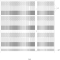
- FIG. 1 shows the structure of a display substrate in the related art, in which each operational amplifier OP is electrically connected to a column of sub-pixels P, and the number of operational amplifiers OP is consistent with the number of sub-pixels P in a row.
- the operational amplifier OP is used to amplify the data signal output by the source driver chip (Source IC) and then provide it to the corresponding connected sub-pixel P.
- Source IC source driver chip
- the refresh rate of the human eye's watching area is greater than the refresh rate of the non-watching area, or not all sub-pixels P are lit, resulting in that operational amplifiers OP corresponding to the non-watching area or the unlit sub-pixel P are idle, causing a waste of resources.
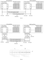
- embodiments of the present disclosure provide a display substrate, as shown in FIGs. 2 to 4 , including:
- the reusing circuit 105 is controlled to conduct one of the data lines 103 connected to it and disconnect the remaining data lines 103 connected to it, so that through the conductive reusing circuit 105 and data line 103, the reusing circuit 105 can provide data signals output by at least two operational amplifiers OP to sub-pixels P in the same column that are electrically connected to the data line 103. In this way, by dynamically gating the idle operational amplifier OP in the related art through the reusing circuit 105, the resource utilization rate of the operational amplifier 104 is improved.
- the reusing circuit 105 can also be controlled to disconnect from all the data lines 103 connected to it, so as to provide the data signal output by each operational amplifier 104 to each column of sub-pixels P electrically connected to the each operational amplifier 104 in a one-to-one correspondence.
- the respective operational amplifiers 104 work independently and are not reused with each other.
- each pixel island 102 may include red sub-pixels r, green sub-pixels g, and blue sub-pixels b.
- the number of red sub-pixels r, green sub-pixels g and blue sub-pixels b is the same.
- the red sub-pixels r are arranged in a row along the row direction X
- the green sub-pixels g are arranged in a row along the row direction X
- the blue sub-pixels b are arranged in a row along the row direction X.
- the rows of red sub-pixels, green sub-pixels and blue sub-pixels are arranged along the column direction Y so that the pixel islands and the sub-pixels P in each pixel island are arranged in an array.
- the reusing circuit 105 includes first sub-reusing circuits 1051.
- the sub-pixels P electrically connected to each first sub-reusing circuit 1051 are located in at least two partitions Z, so as to reuse the operational amplifiers 104 corresponding to sub-pixels P in different partitions Z through the first sub-reusing circuit 1051.
- each first sub-reusing circuit 1051 being connected among two operational amplifiers 104 and the data lines 103 electrically connected to the two operational amplifiers 104, and the sub-pixels P electrically connected to the first sub-reusing circuit 1051 being located in two partitions Z, are taken as an example for description.
- the 1 st to n th partitions arranged continuously are the watching area W, and the (n+1) th to 2n th partitions arranged continuously are the non-watching area NW. Because the watching area W is a continuous range, it can support 1/2 continuous area of the display substrate.
- the sub-pixels P electrically connected to each first sub-reusing circuit 1051 are located in the m th and (m+n) th partitions Z, where m is an integer greater than or equal to 1 and less than or equal to n.
- the m th partition Z is located in the watching area W and the (m+n) th partition Z is located in the non-watching area NW. Therefore, when the non-watching area NW is not refreshed and the watching area W is refreshed, the operational amplifier 104 corresponding to the (m+n) th partition Z in the non-attention area NW to the m th partition Z can be reused in the watching area W through the first sub-reusing circuit 1051, so that the operational amplifier 104 corresponding to the (m+n) th partition Z and the operational amplifier 104 corresponding to the m th partition Z simultaneously provide data signals for the sub-pixels P in the m th partition Z, thereby reducing the charging time and improving the charging rate of the watching area W. In addition, when both the watching area W and the non-watching area NW are refreshed, the operational amplifiers 104 can be used separately in the watching area W and the non-watching area NW, that is, the operational amplifiers are not reused across areas.
- each partition Z includes i columns of pixel islands 102, where i is an integer greater than or equal to 2.
- the first sub-pixels P electrically connected to the first sub-reusing circuit 1051 are located in the j th column of pixel islands 102 of the m th partition and the j th column of pixel islands 102 of the (m+n) th partition, where j is an integer greater than or equal to 1 and less than or equal to i.
- This arrangement not only enables the mutual reusing of the operational amplifier 104 corresponding to the j th column of pixel islands 102 of the m th partition and the operational amplifier 104 corresponding to the j th column of pixel islands 102 of the (m+n) th partition, and can also simplify the wiring method.
- each pixel island 102 is arranged in a single row with k sub-pixels P, where k is an even number.
- Sub-pixels P electrically connected to a first sub-reusing circuit 1051 are at least part of the sub-pixels P in the h th column of the j th column of pixel islands in the m th partition Z, and at least part of the sub-pixels P in the h th column of the j th column of pixel islands in the (m+n) th partition Z.
- h is an integer greater than or equal to 1 and less than or equal to k/4, and an integer greater than or equal to (1+k/4) and less than or equal to (k-4).
- This arrangement can not only reuse the operational amplifier 104 corresponding to the h th column of sub-pixels P of the j th column of pixel islands 102 in the m th partition Z, and the operation amplifier 104 corresponding to the h th column of sub-pixels P of the j th column of pixel islands 102 in the (m+n) th partition Z, but also simplify the wiring method.
- a data line 103 is connected between an operational amplifier 104 and a column of sub-pixels P.
- the sub-pixels P electrically connected to each first sub-reusing circuit 1051 are the h th column of sub-pixels P of the j th column of pixel islands in the m th partition, and the h th column of sub-pixels P of the j th column of pixel islands in the (m+n) th partition.
- the reusing circuit 105 may also include a second sub-reusing circuit 1052.
- Each second sub-reusing circuit 1052 is connected between two columns of sub-pixels P in the same pixel island 102 and between two first sub-reusing circuits 1051 corresponding to the two columns of sub-pixels P.
- the second sub-reusing circuit 1052 can be used to reuse the operational amplifiers 104 respectively corresponding to the two columns of sub-pixels P in the same pixel island 102.
- the first sub-reusing circuit 1051 can realize reusing of the operational amplifiers 104 corresponding to different partitions Z, and it is also compatible with the reusing of operational amplifiers 104 corresponding to two columns of sub-pixels P in the same column of pixel islands 102 in the same partition Z.
- k is a multiple of 4, and h is an integer greater than or equal to 1 and less than or equal to k/4, and an integer greater than or equal to (1+k/4) and less than or equal to (k-4).
- the emitted light rays from the 1 st to (k/2) th sub-pixels P can be converged to the left eye L to form the left eye view point (View), and the emitted light rays from the (1+k/2) th to the k th sub-pixels P can be converged to the right eye R to form a right eye view point (View), to achieve naked-eye 3D display.
- each second sub-reusing circuit 1052 is electrically connected to the h th column and the (h+k/4) th column of sub-pixels P of the same column of pixel islands 102 respectively, so that the operational amplifier 104 corresponding to the h th column of sub-pixels P and the operational amplifier 104 corresponding to the (h+k/4) th column of sub-pixels P in the same column of pixel islands 102 can be reused with each other, which is beneficial to simplifying the wiring design.
- the first sub-reusing circuit 1051 connecting the h th column of sub-pixels P of the j th column of pixel islands 102 in the m th partition Z to the h th column of sub-pixels P of the j th column of pixel islands 102 in the (m+n) th partition Z includes a first transistor M1, a second transistor M2 and a third transistor M3.
- the first sub-reusing circuit 1051 connecting the (h+k/4) th column of sub-pixels P of the j th column of pixel islands 102 in the m th partition Z to the (h+k/4) th column of sub-pixels P of the j th column of pixel islands 102 in the (m+n) th partition Z, includes a fourth transistor M4, a fifth transistor M5 and a sixth transistor M6.
- the second sub-reusing circuit 1052 connecting the h th column and the (h+k/4) th column of sub-pixels P of the j th column of pixel islands 102 in the m th partition Z, includes a seventh transistor M7, an eighth transistor M8 and Ninth transistor M9.
- the second sub-reusing circuit 1052 connecting the h th column and the (h+k/4) th column of sub-pixels P of the j th column of pixel islands 102 in the (m+n) th partition Z, includes a tenth transistor M10, an eleventh transistor M11 and a twelfth transistor M12.
- the gate electrode of the first transistor M1 is electrically connected to the first control signal terminal G1.
- the first electrode of the first transistor M1 is electrically connected to the operational amplifier 104 corresponding to the h th column of sub-pixels P of the j th column of pixel islands 102 in the (m+n) th partition Z.
- the second electrode of the first transistor M2 is electrically connected to the operational amplifier 104 corresponding to the h th column of sub-pixels P of the j th column of pixel islands 102 in the m th partition Z.
- the gate of the second transistor M2 is electrically connected to the second control signal terminal G2.
- the first electrode of the second transistor M2 is electrically connected to the second electrode of the first transistor M1.
- the second electrode of the second transistor M2 is electrically connected to the first electrode of the seventh transistor M7.
- the gate of the third transistor M3 is electrically connected to the third control signal terminal G3.
- the first electrode of the third transistor M3 is electrically connected to the first electrode of the first transistor M1.
- the second electrode of the third transistor M3 is electrically connected to the first electrode of the tenth transistor M10.
- the gate electrode of the fourth transistor M4 is electrically connected to the fourth control signal terminal G4.
- the first electrode of the first transistor M1 is connected to the operational amplifier 104 corresponding to the (h+k/4) th column of sub-pixels P of the j th column of pixel islands 102 in the (m+n) th partition Z.
- the second electrode of the first transistor M1 is electrically connected to the operational amplifier 104 corresponding to the (h+k/4) th column of sub-pixels P of the j th column of pixel islands 102 in the m th partition Z.
- the gate of the fifth transistor M5 is electrically connected to the fifth control signal terminal G5.
- the first electrode of the fifth transistor M5 is electrically connected to the second electrode of the fourth transistor M4.
- the second electrode of the fifth transistor M5 is electrically connected to the first electrode of the eighth transistor M8.
- the gate of the sixth transistor M6 is electrically connected to the sixth control signal terminal G6.
- the first electrode of the sixth transistor M6 is electrically connected to the second electrode of the eleventh transistor M11.
- the second electrode of the sixth transistor M6 is electrically connected to the first electrode of the fourth transistor M4.
- the gate electrode of the seventh transistor M7 is electrically connected to the seventh control signal terminal G7.
- the second electrode of the seventh transistor M7 is electrically connected to the data line 103 corresponding to the h th column of sub-pixels P of the j th column of pixel islands 102 in the m th partition Z.
- the gate electrode of the eighth transistor M8 is electrically connected to the eighth control signal terminal G8.
- the second electrode of the eighth transistor M8 is connected to the data line 103 corresponding to the (h+k/4) th column of sub-pixels P of the j th column of pixel islands 102 in the m th partition Z.
- the gate of the ninth transistor M9 is electrically connected to the ninth control signal terminal G9.
- the first electrode of the ninth transistor M9 is electrically connected to the second electrode of the fourth transistor M4.
- the second electrode of the ninth transistor M9 is electrically connected to the second electrode of the second transistor M2.
- the gate electrode of the tenth transistor M10 is electrically connected to the tenth control signal terminal G10,
- the second electrode of the tenth transistor M10 is electrically connected to the data line 103 corresponding to the h th column of sub-pixels P of the j th column of pixel islands 102 in the (m+n) th partition Z.
- the gate electrode of the eleventh transistor M11 is electrically connected to the eleventh control signal terminal G11.
- the second electrode of the eleventh transistor M11 is connected to the data line 103 corresponding to the (h+k/4) th column of sub-pixels P of the j th column of pixel islands 102 in the (m+n) th partition Z.
- the gate of the twelfth transistor M12 is electrically connected to the twelfth control signal terminal G12.
- the first electrode of the twelfth transistor M12 is electrically connected to the second electrode of the sixth transistor M6.
- the second electrode of the twelfth transistor M12 is electrically connected to the second electrode of the third transistor M3.
- FIG. 7 and FIG. 8 show that the first column of sub-pixels P of the first column of pixel island 102 in the first partition Z, and the first column of sub-pixels P of the first column of pixel island 102 in the ninth partition Z are electrically connected to the same first sub-reusing circuit 1051.
- the fifth column of sub-pixels P of the first column of the pixel island 102 in the first partition Z, and the fifth column of sub-pixels P of the first column of the pixel island 102 in the ninth partition Z are electrically connected to another first sub-reusing circuit 1051.
- FIG. 7 and FIG. 8 show that the first column of sub-pixels P of the first column of pixel island 102 in the first partition Z, and the first column of sub-pixels P of the first column of pixel island 102 in the ninth partition Z are electrically connected to the same first sub-reusing circuit 1051.
- FIG. 7 and FIG. 8 show that the first column of sub-pixels P of the first column of pixel island 102 in the first
- '1' represents a high-level signal and '0' represents a low-level signal.
- Each transistor is turned on under a high-level signal and turned off under a low-level signal.
- '1' and '0' are logic levels, which are only used to better explain the working process of the embodiments of the present disclosure, rather than are the voltages applied to the gate of each transistor during implementations.
- Table 1 exemplarily shows, when transistors in FIG. 7 are applied with different logic levels, the working state of the operational amplifier 104 (i.e., OP1 in Table 1) corresponding to the first column of sub-pixels P in the first column of pixel island 102 in the first partition Z and the working state of the operational amplifier 104 (that is, OP1' in Table 1) corresponding to the first column of sub-pixels P in the first column of the pixel island 102 in the ninth partition Z, the working state of the operation amplifier 104 (i.e., OP5 in Table 1) corresponding to the fifth column of sub-pixels P in the first column of pixel island 102 in the first partition Z, and the working state of the operational amplifier 104 (i.e., OP5' in Table 1) corresponding to the fifth column of sub-pixels P in the first column of pixel island 102 in the ninth partition Z.
- the working state of the operational amplifier 104 i.e., OP1 in Table 1
- the working state of the operational amplifier 104
- the operational amplifier 104 i.e., OP1 in Table 1
- the operational amplifier 104 i.e., OP1' in Table 1
- the operational amplifier 104 i.e., OP1' in Table 1
- the operational amplifier 104 i.e. OP1' in Table 1
- the operational amplifier 104 corresponding to the first column of sub-pixels P in the first column of the pixel island 102 in the ninth partition Z
- the operational amplifier 104 i.e., OP1 in Table 1
- the operational amplifier 104 i.e., OP5 in Table 1
- the operational amplifier 104 i.e., OP5' in Table 1
- the operational amplifier 104 i.e., OP5' in Table 1
- the operational amplifier 104 i.e., OP5' in Table 1
- the operational amplifier 104 i.e., OP5 in Table 1
- the operational amplifier 104 i.e., OP1 in Table 1
- the operational amplifier 104 corresponding to the first column of sub-pixels P in the first column of pixel island 102 in the first partition Z
- the operational amplifier 104 i.e., OP1' in Table 1
- the operational amplifier 104 that is, OP5 in Table 1
- the operational amplifier 104 corresponding to the fifth column of sub-pixels P in the first column of pixel island 102 in the first partition Z
- the operational amplifier 104 that is, OP5 in Table 1
- the operational amplifier 104 i.e., OP5' in Table 1 corresponding to the fifth column of sub-pixels P in the first column of pixel island 102 in the ninth partition Z.
- the operational amplifier 104 i.e., OP1' in Table 1 corresponding to the first column of sub-pixels P in the first column of the pixel island 102 in the ninth partition Z can be reused as the operational amplifier 104 (that is, OP1 in Table 1) corresponding to the first column of sub-pixels P in the first column of the pixel island 102 in the first partition Z, and the operational amplifier 104 (i.e., OP5' in Table 1) corresponding to the fifth column of sub-pixels P in the first column of pixel island 102 in the ninth partition Z can be reused as the operational amplifier 104 (i.e., OP5 in Table 1) corresponding to the fifth column of sub-pixels P in the first column of pixel island 102 in the first partition Z.
- the operational amplifier 104 i.e., OP1' in Table 1 corresponding to the first column of sub-pixels P in the first column of the pixel island 102 in the ninth partition Z and the operational amplifier 104 (i.e., OP1' in Table 1) corresponding to the first column of sub-pixels P in the first column of pixel island 102 in the first partition Z are not reused, and the operational amplifier 104 (i.e., OP5' in Table 1) corresponding to the fifth column of sub-pixels P in the first column of pixel island 102 in the ninth partition Z and the operational amplifiers 104 (i.e., OP5 in Table 1) corresponding to the first column of sub-pixels P in the first column of pixel island 102 in the first partition Z are not reused.
- Table 2-1 and Table 2-2 exemplarily show, when transistors in FIG. 8 are applied with different logic levels, the working state of the operational amplifier 104 (i.e., OP1) corresponding to the first column of sub-pixels P in the first column of pixel island 102 in the first partition Z, the working state of the operational amplifier 104 (i.e., OP1') corresponding to the first column of sub-pixels P in the first column of pixel island 102 in the ninth partition Z, the working state of the operational amplifier 104 (i.e., OP5) corresponding to the fifth column of sub-pixels P in the first column of pixel island 102 in the first partition Z, the working state of the operational amplifier 104 (i.e., OP5') corresponding to the fifth column of sub-pixels P in the first column of pixel island 102 in the ninth partition Z, the working states of the operational amplifiers 104 (i.e., OP1 and OP5) corresponding to the first and fifth columns of sub-pixels P in the first
- the operational amplifier 104 i.e., OP5
- the operational amplifier 104 i.e., OP1
- the operational amplifier 104 i.e., OP1
- the operational amplifier 104 i.e., OP1
- the operational amplifier 104 i.e. OP5
- the operational amplifier 104 i.e. OP5
- the operational amplifier 104 i.e., OP1
- the operational amplifier 104 i.e., OP5
- the operational amplifier 104 i.e., OP5'
- the operational amplifier 104 i.e., OP1'
- the operational amplifier 104 i.e., OP1'
- the operational amplifier 104 i.e., OP5'
- the operational amplifier 104 i.e., OP1'
- the operational amplifier 104 i.e., OP1 corresponding to the first column of sub-pixels P in the first column of the pixel island 102 in the ninth partition Z
- the operational amplifier 104 i.e., OP1
- the operational amplifier 104 i.e., OP1
- the operational amplifier 104 i.e., OP1'
- the operational amplifier 104 i.e., OP5'
- the operational amplifier 104 i.e., OP5 corresponding to the fifth column of sub-pixels P in the first column of pixel island 102 in the ninth partition Z
- the operational amplifier 104 i.e., OP5
- the operational amplifier 104 i.e., OP5
- the operational amplifier 104 i.e., OP5'
- the operational amplifier 104 i.e., OP1'
- the operational amplifier 104 i.e., OP1 corresponding to the first column of sub-pixels P in the first column of pixel island 102 in the ninth partition Z
- the operational amplifier 104 i.e., OP1
- the operational amplifier 104 i.e., OP5'
- the operational amplifier 104 i.e., OP5
- the operational amplifier 104 i.e., OP1
- the operational amplifier 104 corresponding to the first column of sub-pixels P in the first column of the pixel island 102 in the first partition Z can be reused as the operational amplifier 104 (i.e.
- OP1' corresponding to the first column of sub-pixels P in the first column of pixel island 102 in the ninth partition Z
- the operational amplifier 104 i.e., OP5
- the operational amplifier 104 i.e., OP5'
- the second transistor M2 when the third transistor M3, the fifth transistor M5, the sixth transistor M6, the seventh transistor M7, the eighth transistor M8, the tenth transistor M10, and the transistor M11 are turned on, and the other transistors are turned off, none of the operational amplifier 104 (i.e., OP1) corresponding to the first column of sub-pixels P in the first column of the pixel island 102 in the first partition Z, the operational amplifier 104 (i.e., OP5) corresponding to the fifth column of sub-pixels P in the first column of the pixel island 102 in the first partition Z, the operational amplifier 104 (i.e., OP1') corresponding to the first column of sub-pixels P in the first column of the pixel island 102 in the ninth partition Z, and the operational amplifier 104 (i.e., OP5') corresponding to the fifth column of sub-pixels P in the first column of pixel island 102 in the ninth partition Z can be
- FIG. 9 shows a charging simulation diagram using one operational amplifier 104 to provide data signals for sub-pixels P.
- FIG. 10 shows a charging simulation diagram using two operational amplifiers 104 (that is, in the case of reusing) to provide data signals for sub-pixels P.
- an operational amplifier 104 can be connected to a column of sub-pixels P through two data lines 103.
- One of the two data lines 103 connects the sub-pixels P in the odd-numbered rows in a column, and the other data line 103 connects the sub-pixels P of the even-numbered rows in the column.
- the sub-pixels P electrically connected to each first sub-reusing circuit 1051 are the even-numbered rows of sub-pixels P in the h th column of the j th column of pixel island 102 in the m th partition Z, and the even-numbered rows of sub-pixels P in the h th column of the j th column of pixel island 102 in the (m+n) th partition Z.
- the data signal provided by the operational amplifier 104 corresponding to the h th column of sub-pixels P in the j th column of pixel island 102 in the m th partition Z can be written into the even-numbered rows of sub-pixels P in the h th column of the j th column of pixel island 102 in the (m+n) th partition Z.
- the data signal provided by the operational amplifier 104 corresponding to the h th column of sub-pixels P in the j th column of pixel island 102 in the (m+n) th partition Z can be written into the even-numbered rows of sub-pixels P in the h th column of the j th column of pixel island 102 in the m th partition Z through the first sub-reusing circuit 1051. This reduces the charging time of a frame, thereby increasing the frame rate.
- P1 represents the first column of sub-pixels P in the first column of pixel island 102 in the first partition Z
- P1' represents the first column of sub-pixels P in the first column of pixel island 102 in the ninth partition Z.
- the first sub-reusing circuit 1051 includes: a thirteenth transistor M13 and a fourteenth transistor M14.
- the gate electrode of the thirteenth transistor M13 is electrically connected to the thirteenth control signal terminal G13.
- the first electrode of the thirteenth transistor M13 is electrically connected to the operation amplifier 104 corresponding to the h th column of sub-pixels P in the j th column of pixel island 102 in the m th partition Z.
- the second electrode of the thirteenth transistor M13 is electrically connected to the data line 103 corresponding to the even-numbered rows of sub-pixels P of the h th column of the j th column of pixel island 102 in the (m+n) th partition Z.
- the gate electrode of the fourteenth transistor M14 is electrically connected to the fourteenth control signal terminal G14.
- the first electrode of the fourteenth transistor M14 is connected to the operational amplifier 104 corresponding to the h th column of sub-pixels P in the j th column of pixel island 102 in the (m+n) th partition Z.
- the second electrode of the fourteenth transistor M14 is electrically connected to the data line 103 corresponding to the even-numbered rows of sub-pixels P in the h th column of the j th column of pixel island 102 in the m th partition Z.
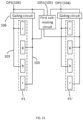
- the above display substrate provided by the embodiments of the present disclosure may also include a plurality of gating circuits 106 located in the frame area BB.
- Each gating circuit 106 is connected to the operational amplifier 104 and two data lines 103 corresponding to the operational amplifier 104.
- the gating circuit 106 can cooperate with the first sub-reusing circuit 105 to realize different row reusing of the operational amplifiers 104 in different partitions Z.
- the gating circuit 106 may include a fifteenth transistor M15 and a sixteenth transistor M16.
- the gate of the fifteenth transistor M15 is electrically connected to the fifteenth control signal terminal G15.
- the first electrode of the fifteenth transistor M15 is electrically connected to an operational amplifier 104.
- the second electrode of the fifteenth transistor M15 is electrically connected to one of the two data lines 103.
- the gate of the sixteenth transistor M16 is electrically connected to the sixteenth control signal terminal G16.
- the first electrode of the sixteenth transistor M16 is electrically connected to an operational amplifier 104, and the second electrode of the sixteenth transistor M16 is electrically connected to the other one of the two data lines.
- FIG. 12 shows that the first column of sub-pixels P in the first column of the pixel island 102 in the first partition Z are electrically connected to the first sub-reusing circuit 1051 through two data lines 103 and a gate circuit 106.
- the first column of sub-pixels P in the first column of the pixel island 102 in the ninth partition Z are electrically connected to the same first sub-reusing circuit 1051 through two data lines 103 and another gate circuit 106.
- '1' represents a high-level signal and '0' represents a low-level signal.
- Each transistor is turned on under a high-level signal and turned off under a low-level signal.
- '1' and '0' are logic levels, which are only used to better explain the working process of the embodiments of the present disclosure, rather than are the voltages applied to the gate of each transistor during implementations.
- Table 3 exemplarily shows when each transistor in FIG. 12 is applied with different logic levels, the working state of the operational amplifier 104 (i.e., OP1) corresponding to the first column of sub-pixels P of the first column of pixel island 102 in the first partition Z, and the working state of the operational amplifier 104 (i.e., OP1') corresponding to the first column of sub-pixels P in the first column of the pixel island 102 in the ninth partition Z.
- the working state of the operational amplifier 104 i.e., OP1
- OP1' working state of the operational amplifier 104
- the operational amplifier 104 i.e., OP1
- the operational amplifier 104 i.e., OP1
- the operational amplifier 104 can be reused as the operational amplifier 104 (i.e., OP1') corresponding to the even-numbered row of sub-pixels P in the first column of the pixel island
- the operational amplifier 104 i.e., OP1
- the fifteenth transistor M15 in the gate circuit 106 corresponding to the first column of the sub-pixels P in the first column of the pixel island 102 in the first partition Z, and the fifteenth transistor M15 (i.e., M15') in the gating circuit 106 corresponding to the first column of the sub-pixels P in the first column of the pixel island 102 in the ninth partition Z are both turned on, so that data signals of the operational amplifier 104 (i.e., OP1) corresponding to the first column of sub-pixels P in the first column of pixel island 102 in the first partition Z, and data signals of the operational amplifier 104 (i.e.
- the sixteenth transistor M16 in the gating circuit 106 corresponding to the first column of sub-pixels P in the first column of pixel island 102 in the first partition Z, and the sixteenth transistor M16 (i.e., M16' ) in the gating circuit 106 corresponding to the first column of sub-pixels P of the first column of pixel island 102 in the ninth partition Z are both turned on, so that data signals of the operational amplifier 104 (i.e., OP1) corresponding to the first column of sub-pixels P in the first column of pixel island 102 in the first partition Z, and data signals of the operational amplifier 104 (i.e.
- k sub-pixels P are arranged in a single row of each pixel island 102, and k is a multiple of 4.
- the reusing circuit 105 includes a third sub-reusing circuits 1053.
- Sub-pixels P electrically connected to the third sub-reusing circuit 1053 are the sub-pixels P of the h th column and the sub-pixels P of the (h+k/4) th column in the same column of pixel island 102.
- h is an integer greater than or equal to 1 and less than or equal to k/4, and an integer greater than or equal to (1+k/4) and less than or equal to (k-4); such that the operational amplifier 104 corresponding to the h th column of sub-pixels P in one column of pixel island 102 and the operational amplifier 104 corresponding to the (h+k/4) th column of sub-pixels P in the same one column of pixel island 102 can be reused with each other, which is beneficial to simplifying the wiring design.
- each adjacent i columns of pixel islands 102 in the row direction X forms one partition Z, and there are 2n partitions Z in the row direction X, where i is an integer greater than or equal to 2, and n is a positive integer.
- the reusing circuit 105 further includes a fourth sub-reusing circuit 1054.
- the fourth sub-reusing circuit 1054 connects sub-pixels P which are in the same column (e.g., the h th column) of the same column (e.g., the j th column, j is an integer greater than or equal to 1, and less than or equal to i) of pixel island 102 respectively in the m th and (m+n) th partitions Z.
- m is an integer greater than or equal to 1 and less than or equal to n.
- the third sub-reusing circuit 1053 connecting the h th column of sub-pixels P and the (h+k/4) th column of sub-pixels P in the j th column of pixel island 102 in the m th partition Z, includes a seventeenth transistor M17, an eighteenth transistor M18, a nineteenth transistor M19, a twentieth transistor M20 and a twenty-first transistor M21, j is an integer greater than or equal to 1 and less than or equal to i.
- the third sub-reusing circuit 1053 connecting the h th column of sub-pixels P and the (h+k/4) th column of sub-pixels P in the j th column of pixel island 102 in the (m+n) th partition Z, includes a twenty-second transistor M22, a twenty-third transistor M23, a twenty-fourth transistor M24, a twenty-fifth transistor M25 and the twenty-sixth transistor M26.
- the fourth sub-reusing circuit 1054 connecting the h th column of sub-pixels P in the j th column of pixel island 102 in the m th partition Z and the h th column of sub-pixels P of the j th column of pixel island 102 in the (m+n) th partition Z includes a twenty-seventh transistor M27.
- the fourth sub-reusing circuit 1054 connecting the (h+k/4) th column of sub-pixels P in the j th column of pixel island 102 in the m th partition Z and the (h+k/4) th column of sub-pixels P of the j th column of pixel island 102 in the (m+n) th partition Z includes the twenty-eighth transistor M28.
- the gate of the seventeenth transistor M17 is electrically connected to the seventeenth control signal terminal G17.
- the first electrode of the seventeenth transistor M17 is electrically connected to the second electrode of the eighteenth transistor M18.
- the second electrode of the seventeenth transistor M17 is electrically connected to the data line 103 corresponding to the h th column of sub-pixels P in the j th column of pixel island 102 in the m th partition Z.
- the gate electrode of the eighteenth transistor M18 is electrically connected to the eighteenth control signal terminal G18.
- the first electrode of the eighteenth transistor M18 is electrically connected to the operation amplifier 104 corresponding to the h th column of sub-pixels P in the j th column of pixel island 102 in the m th partition Z.
- the gate of the nineteenth transistor M19 is electrically connected to the nineteenth control signal terminal G19.
- the first electrode of the nineteenth transistor M19 is electrically connected to the second electrode of the twentieth transistor M20, and the second electrode of the nineteenth transistor M19 is electrically connected to the data line 103 corresponding to the (h+k/4) th column of sub-pixels P in the j th column of pixel island 102 in the m th partition Z.
- the gate of the twentieth transistor M20 is electrically connected to the twentieth control signal terminal G20.
- the first electrode of the twentieth transistor M20 is electrically connected to the operational amplifier 104 corresponding to the (h+k/4) th column of sub-pixels P in the j th column of pixel island 102 in the m th partition Z.
- the gate of the twenty-first transistor M21 is electrically connected to the twenty-first control signal terminal G21.
- the first electrode of the twenty-first transistor M21 is electrically connected to the second electrode of the twentieth transistor M20.
- the second electrode of the twenty-first transistor M21 is electrically connected to the second electrode of the eighteenth transistor M18.
- the gate of the twenty-second transistor M22 is electrically connected to the twenty-second control signal terminal G22.
- the first electrode of the twenty-second transistor M22 is electrically connected to the second electrode of the twenty-third transistor M23.
- the second electrode of M22 is electrically connected to the data line 103 corresponding to the h th column of sub-pixels P in the j th column of pixel island 102 in the (m+n) th partition Z.
- the gate electrode of the twenty-third transistor M23 is electrically connected to the twenty-third control signal terminal G23.
- the first electrode of the twenty-third transistor M23 is electrically connected to the operational amplifier 104 corresponding to the h th column of sub-pixels P in the j th column of pixel island 102 in the m th partition Z.
- the gate of the twenty-fourth transistor M24 is electrically connected to the twenty-fourth control signal terminal G24.
- the first electrode of the twenty-fourth transistor M24 is electrically connected to the second electrode of the twenty-fifth transistor M25.
- the second electrode of the twenty-fourth transistor M24 is electrically connected to the data line 103 corresponding to the (h+k/4) th column of sub-pixels P in the j th column of pixel island 102 in the m th partition Z.
- the gate electrode of the twenty-fifth transistor M25 is electrically connected to the twenty-fifth control signal terminal G25.
- the first electrode of the twenty-fifth transistor M25 is electrically connected to the operational amplifier 104 corresponding to the (h+k/4) th column of sub-pixels P in the j th column of pixel island 102 in the m th partition Z.
- the gate of the twenty-sixth transistor M26 is electrically connected to the twenty-sixth control signal terminal G26.
- the first electrode of the twenty-sixth transistor M26 is electrically connected to the second electrode of the twenty-fifth transistor M25.
- the second electrode of the twenty-sixth transistor M26 is electrically connected to the second electrode of the twenty-third transistor M23.
- the gate electrode of the twenty-seventh transistor M27 is electrically connected to the twenty-seventh control signal terminal G27.
- the first electrode of the twenty-seventh transistor M27 is electrically connected to the operational amplifier 104 corresponding to the h th column of sub-pixels P in the j th column of pixel island 102 in the (m+n) th partition Z.
- the second electrode of the twenty-seventh transistor M27 is electrically connected to the operational amplifier 104 corresponding to the h th column of sub-pixels P in the j th column of pixel island 102 in the m th partition Z.
- the gate electrode of the twenty-eighth transistor M28 is electrically connected to the twenty-eighth control signal terminal G28.
- the first electrode of the twenty-eighth transistor M28 is electrically connected to the operational amplifier 104 corresponding to the (h+k/4) th column of sub-pixels P in the j th column of pixel island 102 in the (m+n) th partition Z.
- the second electrode of the twenty-eighth transistor M28 is electrically connected to the operational amplifier 104 corresponding to the (h+k/4) th column of sub-pixels P in the j th column of pixel island 102 in the m th partition Z.
- FIG. 15 shows that the first column of sub-pixels P and the fifth column of sub-pixels P in the first column of pixel island 102 in the first partition Z are electrically connected to the same third sub-reusing circuit 1053.
- '1' represents a high-level signal and '0' represents a low-level signal.
- Each transistor is turned on under a high-level signal and turned off under a low-level signal.
- '1' and '0' are logic levels, which are only used to better explain the working process of the embodiments of the present disclosure, rather than are the voltages applied to the gate of each transistor during implementations.
- Table 4 exemplarily shows when each transistor in FIG. 15 is applied with different logic levels, the working state of the operational amplifier 104 (i.e., OP1) corresponding to the first column of sub-pixels P in the first column of pixel island 102 in the first partition Z, and the working state of the operational amplifier 104 (i.e., OP5) corresponding to the fifth column of sub-pixels P in the first column of pixel island 102 in the first partition Z.
- the working state of the operational amplifier 104 i.e., OP1
- OP5 working state of the operational amplifier 104
- the operational amplifier 104 i.e., OP5
- the operational amplifier 104 i.e., OP1
- the operational amplifier 104 i.e., OP1
- the operational amplifier 104 i.e., OP1
- the operational amplifier 104 i.e., OP5
- the operational amplifier 104 i.e., OP5
- the operational amplifier 104 i.e., OP1 corresponding to the first column of sub-pixels P in the first column of the pixel island 102 in the first partition Z
- the operational amplifier 104 i.e., OP5
- the operational amplifier 104 i.e., OP5
- Table 5-1 and Table 5-2 exemplarily show when each transistor in FIG. 16 is applied with different logic levels, the working state of the operational amplifier 104 (i.e., OP1) corresponding to the first column of sub-pixels P in the first column of pixel island 102 in the first partition Z, the working state of the operational amplifier 104 (i.e., OP1') corresponding to the first column of sub-pixels P in the first column of pixel island 102 in the ninth partition Z; the working state of the operational amplifier 104 (i.e., OP5) corresponding to the fifth column of sub-pixels P in the first column of pixel island 102 in the first partition Z, the working state of the operational amplifier 104 (i.e., OP5') corresponding to the fifth column of sub-pixels P in the first column of pixel island 102 in the ninth partition Z; the working state of the operational amplifiers 104 (i.e., OP1 and OP5) corresponding to the first and fifth columns of sub-pixels P in the first column
- the operational amplifier 104 i.e., OP5
- the operational amplifier 104 i.e., OP1
- the operational amplifier 104 i.e., OP1
- the operational amplifier 104 i.e., OP5
- the operational amplifier 104 i.e., OP5
- the operational amplifier 104 i.e., OP1
- the operational amplifier 104 i.e., OP5
- the operational amplifier 104 i.e., OP5
- the operational amplifier 104 i.e., OP5'
- the operational amplifier 104 i.e., OP1'
- the operational amplifier 104 i.e., OP1'
- the operational amplifier 104 i.e., OP5'
- the operational amplifier 104 i.e., OP1'
- the operational amplifier 104 i.e., OP5'
- the operational amplifier 104 i.e., OP1'
- the operational amplifier 104 i.e., OP1 corresponding to the first column of sub-pixels P in the first column of pixel island 102 in the ninth partition Z
- the operational amplifier 104 i.e., OP1
- the operational amplifier 104 i.e., OP1
- the operational amplifier 104 i.e., OP1'
- the operational amplifier 104 i.e., OP5'
- the operational amplifier 104 i.e., OP5 corresponding to the fifth column of sub-pixels P in the first column of the pixel island 102 in the ninth partition Z
- the operational amplifier 104 i.e., OP5
- the operational amplifier 104 i.e., OP5
- the operational amplifier 104 i.e., OP5'
- the operational amplifier 104 i.e., OP1'
- the operational amplifier 104 i.e., OP1 corresponding to the first column of sub-pixels P in the first column of pixel island 102 in the ninth partition Z
- the operational amplifier 104 i.e., OP1
- the operational amplifier 104 i.e., OP5'
- the operational amplifier 104 i.e., OP5'
- the operational amplifier 104 i.e., OP1
- the operational amplifier 104 i.e., OP5'
- the operational amplifier 104 i.e., OP5'
- the operational amplifier 104 i.e., OP5'
- the operational amplifier 104 i.e., OP1 corresponding to the first column of sub-pixels P in the first column of the pixel island 102 in the first partition Z
- the operational amplifier 104 i.e., OP5
- the operational amplifier 104 i.e., OP1'
- the operational amplifier 104 i.e., OP5'
- each transistor may be a top-gate transistor or a bottom-gate transistor, which is not limited here.
- each transistor may be a field effect transistor, a low temperature polysilicon transistor, an amorphous silicon transistor, an oxide transistor, etc.
- the first electrode and the second electrode of each transistor are the drain electrode and the source electrode, and are not distinguished here.
- the above-mentioned display substrate provided by the embodiments of the present disclosure may also include a source driver chip (Source IC) located in the frame area BB.
- the plurality of gate circuits 106, the plurality of reusing circuits 105, and the plurality of operational amplifiers 104 may be integrated in the source driver chip to reduce the loss (RC loading) of the data signal on the transmission path from the source driver chip to the sub-pixels P. It should be understood that when the operational amplifiers 104 are reused among the partitions Z, compared to the case where the operational amplifiers 104 are reused within the pixel island 102, the wiring distance between the two operational amplifiers 104 among partitions Z is longer.
- the gate circuits 106, the reusing circuits 105, and the operational amplifiers 104 are suitable to integrate the gate circuits 106, the reusing circuits 105, and the operational amplifiers 104 in the source driver chip.
- the operational amplifiers 104 are reused within the pixel island 102, the wiring distance between the two operational amplifiers 104 is relatively short.
- the gate circuits 106, the reusing circuits 105, and the operational amplifiers 104 can be integrated into the source driver chip; or the gate circuits 106, the reusing circuits 105, and the operational amplifiers 104 can also be fabricated on the display substrate, which is not specifically limited here.
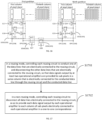
- embodiments of the present disclosure provide a driving method for the above-mentioned display substrate. Since the principle of solving the problem of this driving method is similar to the principle of solving the problem of the above-mentioned display substrate, the implementations of the driving method provided by the embodiments of the present disclosure can be referred to the implementations of the above-mentioned display substrate provided by the embodiments of the present disclosure, and repeated details will not be described again.
- embodiments of the present disclosure provide a driving method for the above-mentioned display substrate, as shown in Figure 17 , including the following steps.
- embodiments of the disclosure provide a display device, including the above display substrate provided by embodiments of the disclosure. Since the principle of solving the problem of the display device is similar to the principle of solving the problem of the above-mentioned display substrate, the implementations of the display device provided by the embodiments of the present disclosure can be referred to the implementations of the above-mentioned display substrate provided by the embodiments of the present disclosure, and the duplication will not be repeated.
- the above-mentioned display device provided by the embodiments of the present disclosure may be: a mobile phone, a tablet computer, a television, a monitor, a notebook computer, a digital photo frame, a navigator, a smart watch, a fitness wristband, a personal digital assistant, or any other device with a product or component that has display functionality.
- the display device includes but is not limited to: a radio frequency unit, a network module, an audio output & input unit, a sensor, a display unit, a user input unit, an interface unit, a memory, a processor, a power supply and other components.
- the above structure does not constitute a limitation on the above display device provided by the embodiments of the present disclosure.
- the above display device provided by the embodiments of the present disclosure may include more or less of the above components, or combinations of certain components, or different arrangements of components.
Landscapes
- Engineering & Computer Science (AREA)
- Physics & Mathematics (AREA)
- Computer Hardware Design (AREA)
- General Physics & Mathematics (AREA)
- Theoretical Computer Science (AREA)
- Control Of Indicators Other Than Cathode Ray Tubes (AREA)
- Liquid Crystal Display Device Control (AREA)
- Devices For Indicating Variable Information By Combining Individual Elements (AREA)
Applications Claiming Priority (1)
| Application Number | Priority Date | Filing Date | Title |
|---|---|---|---|
| PCT/CN2021/133903 WO2023092539A1 (zh) | 2021-11-29 | 2021-11-29 | 显示基板、其驱动方法及显示装置 |
Publications (2)
| Publication Number | Publication Date |
|---|---|
| EP4339929A1 true EP4339929A1 (de) | 2024-03-20 |
| EP4339929A4 EP4339929A4 (de) | 2024-08-07 |
Family
ID=86538710
Family Applications (1)
| Application Number | Title | Priority Date | Filing Date |
|---|---|---|---|
| EP21965272.4A Pending EP4339929A4 (de) | 2021-11-29 | 2021-11-29 | Anzeigesubstrat und ansteuerungsverfahren dafür sowie anzeigevorrichtung |
Country Status (6)
| Country | Link |
|---|---|
| US (1) | US12437695B2 (de) |
| EP (1) | EP4339929A4 (de) |
| JP (1) | JP2024541789A (de) |
| KR (1) | KR102914092B1 (de) |
| CN (1) | CN116529808B (de) |
| WO (1) | WO2023092539A1 (de) |
Family Cites Families (25)
| Publication number | Priority date | Publication date | Assignee | Title |
|---|---|---|---|---|
| US7102608B2 (en) * | 2002-06-21 | 2006-09-05 | Himax Technologies, Inc. | Method and related apparatus for driving pixels located in a row of an LCD panel toward the same average voltage value |
| JP4905484B2 (ja) * | 2009-03-06 | 2012-03-28 | セイコーエプソン株式会社 | 集積回路装置、電気光学装置及び電子機器 |
| CN101847378B (zh) * | 2009-03-27 | 2012-07-04 | 北京京东方光电科技有限公司 | 源极驱动芯片 |
| US9305492B2 (en) | 2012-08-02 | 2016-04-05 | Sharp Kabushiki Kaisha | Display device and method for driving the same |
| CN102854648B (zh) * | 2012-09-21 | 2015-04-08 | 京东方科技集团股份有限公司 | 显示面板及显示装置 |
| CN103152594B (zh) * | 2013-02-20 | 2015-04-01 | 京东方科技集团股份有限公司 | 一种3d显示控制方法及装置 |
| CN104392685B (zh) | 2014-12-15 | 2017-06-09 | 合肥京东方光电科技有限公司 | 阵列基板、显示面板和极性反转驱动方法 |
| WO2016140281A1 (ja) * | 2015-03-02 | 2016-09-09 | シャープ株式会社 | アクティブマトリクス基板、及びそれを備えた表示装置 |
| JP6411257B2 (ja) * | 2015-03-19 | 2018-10-24 | 株式会社ジャパンディスプレイ | 表示装置及びその制御方法 |
| KR102470761B1 (ko) | 2015-07-29 | 2022-11-24 | 삼성전자주식회사 | 출력 신호의 슬루 레이트를 향상시키는 버퍼 증폭기 회로와 이를 포함하는 장치들 |
| CN105187035A (zh) * | 2015-07-31 | 2015-12-23 | 武汉光迅科技股份有限公司 | 一种基于液晶技术的多通道波长选择开关驱动电路 |
| CN105528988B (zh) | 2016-02-15 | 2018-09-11 | 京东方科技集团股份有限公司 | 一种栅极驱动电路、触控显示面板及显示装置 |
| KR102562645B1 (ko) * | 2016-05-20 | 2023-08-02 | 삼성전자주식회사 | 휘도에 따른 디스플레이 구동 방법과, 이를 지원하는 디스플레이 구동 회로 및 전자 장치 |
| CN106356032B (zh) | 2016-11-15 | 2019-03-12 | 武汉华星光电技术有限公司 | 伽马校正电路及其操作方法 |
| KR102615855B1 (ko) * | 2017-01-25 | 2023-12-21 | 삼성전자주식회사 | 표시 설정에 따른 디스플레이 구동 방법 및 이를 지원하는 전자 장치 |
| KR102318387B1 (ko) * | 2017-03-14 | 2021-10-28 | 삼성전자주식회사 | 표시 설정에 따른 감마 전압 운용 방법 및 이를 지원하는 전자 장치 |
| CN106683609B (zh) * | 2017-03-29 | 2020-02-18 | 京东方科技集团股份有限公司 | 一种像素驱动电路及其驱动方法、显示装置 |
| US10755662B2 (en) * | 2017-04-28 | 2020-08-25 | Samsung Electronics Co., Ltd. | Display driving circuit and operating method thereof |
| KR102442114B1 (ko) * | 2017-12-20 | 2022-09-07 | 삼성전자주식회사 | 이미지의 특성에 기반하여 픽셀의 소스 구동을 제어하기 위한 전자 장치 및 전자 장치를 이용한 영상 출력 방법 |
| CN110379383B (zh) | 2019-06-10 | 2021-05-04 | 惠科股份有限公司 | 参考电压产生电路及显示装置 |
| US11386863B2 (en) | 2019-07-17 | 2022-07-12 | Novatek Microelectronics Corp. | Output circuit of driver |
| CN113424251B (zh) * | 2019-11-08 | 2022-05-24 | 京东方科技集团股份有限公司 | 阵列基板及显示装置 |
| CN111261125B (zh) | 2020-03-19 | 2021-10-22 | 合肥京东方显示技术有限公司 | 数据驱动器及其控制方法、显示装置 |
| CN111429802A (zh) * | 2020-03-23 | 2020-07-17 | 武汉华星光电半导体显示技术有限公司 | 显示装置及电子设备 |
| CN113282175B (zh) * | 2021-06-09 | 2024-03-15 | 京东方科技集团股份有限公司 | 显示控制系统、显示控制方法、电子设备、存储介质 |
-
2021
- 2021-11-29 EP EP21965272.4A patent/EP4339929A4/de active Pending
- 2021-11-29 US US18/580,700 patent/US12437695B2/en active Active
- 2021-11-29 JP JP2024503756A patent/JP2024541789A/ja active Pending
- 2021-11-29 KR KR1020247002104A patent/KR102914092B1/ko active Active
- 2021-11-29 CN CN202180003629.XA patent/CN116529808B/zh active Active
- 2021-11-29 WO PCT/CN2021/133903 patent/WO2023092539A1/zh not_active Ceased
Also Published As
| Publication number | Publication date |
|---|---|
| US20240339065A1 (en) | 2024-10-10 |
| KR102914092B1 (ko) | 2026-01-16 |
| JP2024541789A (ja) | 2024-11-13 |
| WO2023092539A1 (zh) | 2023-06-01 |
| KR20240118736A (ko) | 2024-08-05 |
| US12437695B2 (en) | 2025-10-07 |
| CN116529808B (zh) | 2026-01-23 |
| EP4339929A4 (de) | 2024-08-07 |
| CN116529808A (zh) | 2023-08-01 |
Similar Documents
| Publication | Publication Date | Title |
|---|---|---|
| EP1361505B1 (de) | Flüssigkristall-Anzeige mit zwei Bildschirmen und Steuerverfahren dafür | |
| CN111522161B (zh) | 一种阵列基板、显示面板、显示装置及驱动方法 | |
| US11200847B2 (en) | Display panel, display device and drive method | |
| CN107886924B (zh) | 一种显示面板、显示装置及驱动方法 | |
| CN109872700B (zh) | 一种显示模组及其驱动方法、显示装置 | |
| CN110060575A (zh) | 一种显示面板、包含其的显示装置 | |
| US10535321B2 (en) | Display panel, display device and driving method of display panel | |
| CN108091310B (zh) | 一种显示面板、显示装置及驱动方法 | |
| US10971091B2 (en) | Array substrate, display panel and driving method thereof, and display device | |
| CN107978288B (zh) | 一种显示面板、显示装置及驱动方法 | |
| US6605902B2 (en) | Display and electronic device | |
| CN111223463A (zh) | 显示面板及其驱动方法和显示装置 | |
| CN111009224A (zh) | 显示面板的驱动方法、显示装置 | |
| WO2024060363A1 (zh) | 显示面板及显示装置 | |
| US20240169952A1 (en) | Display panel and display device | |
| CN211980170U (zh) | 一种显示屏结构 | |
| EP4339929A1 (de) | Anzeigesubstrat und ansteuerungsverfahren dafür sowie anzeigevorrichtung | |
| CN202473182U (zh) | 一种平板显示装置 | |
| CN111477144A (zh) | 一种显示屏结构及其驱动方法 | |
| CN111477145A (zh) | 一种优化功耗的显示屏结构及其驱动方法 | |
| CN205564250U (zh) | 一种显示屏 | |
| CN212084637U (zh) | 一种省功耗的显示屏结构 | |
| CN216487050U (zh) | 一种特殊显示屏结构 | |
| CN115206257B (zh) | 一种显示面板及终端设备 | |
| CN212675824U (zh) | 一种Demux显示屏 |
Legal Events
| Date | Code | Title | Description |
|---|---|---|---|
| STAA | Information on the status of an ep patent application or granted ep patent |
Free format text: STATUS: THE INTERNATIONAL PUBLICATION HAS BEEN MADE |
|
| PUAI | Public reference made under article 153(3) epc to a published international application that has entered the european phase |
Free format text: ORIGINAL CODE: 0009012 |
|
| STAA | Information on the status of an ep patent application or granted ep patent |
Free format text: STATUS: REQUEST FOR EXAMINATION WAS MADE |
|
| 17P | Request for examination filed |
Effective date: 20231215 |
|
| AK | Designated contracting states |
Kind code of ref document: A1 Designated state(s): AL AT BE BG CH CY CZ DE DK EE ES FI FR GB GR HR HU IE IS IT LI LT LU LV MC MK MT NL NO PL PT RO RS SE SI SK SM TR |
|
| A4 | Supplementary search report drawn up and despatched |
Effective date: 20240708 |
|
| RIC1 | Information provided on ipc code assigned before grant |
Ipc: G06F 3/01 20060101ALI20240702BHEP Ipc: G06F 3/14 20060101ALI20240702BHEP Ipc: G09G 3/3258 20160101ALI20240702BHEP Ipc: G09G 3/325 20160101ALI20240702BHEP Ipc: G09G 3/3225 20160101AFI20240702BHEP |
|
| DAV | Request for validation of the european patent (deleted) | ||
| DAX | Request for extension of the european patent (deleted) |