EP4343373A1 - Bilderfassungsvorrichtung, elektronische vorrichtung damit und ansteuerungsverfahren für bilderfassungsvorrichtung - Google Patents
Bilderfassungsvorrichtung, elektronische vorrichtung damit und ansteuerungsverfahren für bilderfassungsvorrichtung Download PDFInfo
- Publication number
- EP4343373A1 EP4343373A1 EP23197108.6A EP23197108A EP4343373A1 EP 4343373 A1 EP4343373 A1 EP 4343373A1 EP 23197108 A EP23197108 A EP 23197108A EP 4343373 A1 EP4343373 A1 EP 4343373A1
- Authority
- EP
- European Patent Office
- Prior art keywords
- transparent electrode
- diffuser
- mode
- image sensing
- damaged
- Prior art date
- Legal status (The legal status is an assumption and is not a legal conclusion. Google has not performed a legal analysis and makes no representation as to the accuracy of the status listed.)
- Granted
Links
Images





Classifications
-
- G—PHYSICS
- G01—MEASURING; TESTING
- G01S—RADIO DIRECTION-FINDING; RADIO NAVIGATION; DETERMINING DISTANCE OR VELOCITY BY USE OF RADIO WAVES; LOCATING OR PRESENCE-DETECTING BY USE OF THE REFLECTION OR RERADIATION OF RADIO WAVES; ANALOGOUS ARRANGEMENTS USING OTHER WAVES
- G01S7/00—Details of systems according to groups G01S13/00, G01S15/00, G01S17/00
- G01S7/48—Details of systems according to groups G01S13/00, G01S15/00, G01S17/00 of systems according to group G01S17/00
- G01S7/497—Means for monitoring or calibrating
-
- G—PHYSICS
- G01—MEASURING; TESTING
- G01R—MEASURING ELECTRIC VARIABLES; MEASURING MAGNETIC VARIABLES
- G01R19/00—Arrangements for measuring currents or voltages or for indicating presence or sign thereof
- G01R19/0038—Circuits for comparing several input signals and for indicating the result of this comparison, e.g. equal, different, greater, smaller (comparing pulses or pulse trains according to amplitude)
-
- G—PHYSICS
- G01—MEASURING; TESTING
- G01S—RADIO DIRECTION-FINDING; RADIO NAVIGATION; DETERMINING DISTANCE OR VELOCITY BY USE OF RADIO WAVES; LOCATING OR PRESENCE-DETECTING BY USE OF THE REFLECTION OR RERADIATION OF RADIO WAVES; ANALOGOUS ARRANGEMENTS USING OTHER WAVES
- G01S17/00—Systems using the reflection or reradiation of electromagnetic waves other than radio waves, e.g. lidar systems
- G01S17/88—Lidar systems specially adapted for specific applications
- G01S17/89—Lidar systems specially adapted for specific applications for mapping or imaging
-
- G—PHYSICS
- G01—MEASURING; TESTING
- G01S—RADIO DIRECTION-FINDING; RADIO NAVIGATION; DETERMINING DISTANCE OR VELOCITY BY USE OF RADIO WAVES; LOCATING OR PRESENCE-DETECTING BY USE OF THE REFLECTION OR RERADIATION OF RADIO WAVES; ANALOGOUS ARRANGEMENTS USING OTHER WAVES
- G01S17/00—Systems using the reflection or reradiation of electromagnetic waves other than radio waves, e.g. lidar systems
- G01S17/88—Lidar systems specially adapted for specific applications
- G01S17/89—Lidar systems specially adapted for specific applications for mapping or imaging
- G01S17/894—Three-dimensional [3D] imaging with simultaneous measurement of time-of-flight at a two-dimensional [2D] array of receiver pixels, e.g. time-of-flight cameras or flash lidar
-
- G—PHYSICS
- G01—MEASURING; TESTING
- G01S—RADIO DIRECTION-FINDING; RADIO NAVIGATION; DETERMINING DISTANCE OR VELOCITY BY USE OF RADIO WAVES; LOCATING OR PRESENCE-DETECTING BY USE OF THE REFLECTION OR RERADIATION OF RADIO WAVES; ANALOGOUS ARRANGEMENTS USING OTHER WAVES
- G01S7/00—Details of systems according to groups G01S13/00, G01S15/00, G01S17/00
- G01S7/48—Details of systems according to groups G01S13/00, G01S15/00, G01S17/00 of systems according to group G01S17/00
- G01S7/481—Constructional features, e.g. arrangements of optical elements
- G01S7/4811—Constructional features, e.g. arrangements of optical elements common to transmitter and receiver
- G01S7/4813—Housing arrangements
-
- G—PHYSICS
- G01—MEASURING; TESTING
- G01S—RADIO DIRECTION-FINDING; RADIO NAVIGATION; DETERMINING DISTANCE OR VELOCITY BY USE OF RADIO WAVES; LOCATING OR PRESENCE-DETECTING BY USE OF THE REFLECTION OR RERADIATION OF RADIO WAVES; ANALOGOUS ARRANGEMENTS USING OTHER WAVES
- G01S7/00—Details of systems according to groups G01S13/00, G01S15/00, G01S17/00
- G01S7/48—Details of systems according to groups G01S13/00, G01S15/00, G01S17/00 of systems according to group G01S17/00
- G01S7/483—Details of pulse systems
- G01S7/486—Receivers
- G01S7/487—Extracting wanted echo signals, e.g. pulse detection
- G01S7/4876—Extracting wanted echo signals, e.g. pulse detection by removing unwanted signals
-
- G—PHYSICS
- G01—MEASURING; TESTING
- G01S—RADIO DIRECTION-FINDING; RADIO NAVIGATION; DETERMINING DISTANCE OR VELOCITY BY USE OF RADIO WAVES; LOCATING OR PRESENCE-DETECTING BY USE OF THE REFLECTION OR RERADIATION OF RADIO WAVES; ANALOGOUS ARRANGEMENTS USING OTHER WAVES
- G01S7/00—Details of systems according to groups G01S13/00, G01S15/00, G01S17/00
- G01S7/48—Details of systems according to groups G01S13/00, G01S15/00, G01S17/00 of systems according to group G01S17/00
- G01S7/497—Means for monitoring or calibrating
- G01S2007/4975—Means for monitoring or calibrating of sensor obstruction by, e.g. dirt- or ice-coating, e.g. by reflection measurement on front-screen
Definitions
- the present disclosure relates to an image sensing apparatus, an electronic apparatus including the same, and a driving method of the image sensing apparatus.
- An image sensor is a device that converts an optical image into an electrical signal.
- image sensors Recently, with the development of computer industry and communications industry, demand for image sensors has increased in various fields such as digital cameras, camcorders, personal communication systems (PCSs), game devices, security cameras, medical micro cameras, and robot vacuum cleaners.
- PCSs personal communication systems
- Image sensors typically measure a depth using the triangulation, Time of Flight (ToF), and interferometry methods, of which the ToF method has a wide application range and fast processing speed, and is also advantageous in terms of cost.
- An image sensor based on the ToF calculates a distance to a target object by measuring a time until a pulseshaped optical signal emitted from a light source is reflected by the target object and returns, and accordingly, an image for the depth of the target object is generated.
- This image sensor includes a diffuser that is located in a path in which an optical signal is emitted and incident and spreads the optical signal in a Field of View (FoV) area, a transparent electrode determining damage, cracks, or separation of the diffuser is applied on the diffuser, and a transparent electrode film shielding electromagnetic interference noise radiated through the path through which the optical signal is emitted and incident may be applied on the diffuser.
- the transparent electrode determining damage, cracks, or separation of the diffuser and the transparent electrode film shielding electromagnetic interference noise are implemented as separate components.
- the present disclosure is to directed to an image sensing apparatus, an electronic apparatus including the same, and a driving method of the image sensing apparatus, for not only determining whether damage, cracks, or separation of a diffuser occur but also shielding electromagnetic interference noise using a transparent electrode located on the diffuser.
- the image sensing apparatus as disclosed herein may be configured to perform the image sensing method as disclosed herein. Alternatively or additionally, the image sensing method as disclosed herein may be such to be performed using the image sensing apparatus as disclosed herein. Any, some or all of the additional features of the image sensing method as disclosed herein may be applicable also to the image sensing apparatus unless indicated otherwise or technically inappropriate. Any, some or all of the additional features of the image sensing apparatus as disclosed herein may be applicable also to the image sensing method, unless indicated otherwise or technically inappropriate.
- An image sensing apparatus may include a driver disposed on a substrate and configured to drive a light emitter and a light receiver to emit a first optical signal toward an object and receive a second optical signal reflected from the object, a housing coupled to the substrate and surrounding the light emitter, the light receiver, and the driver, a diffuser disposed on the housing, and a transparent electrode disposed on the diffuser, wherein the driver includes a transparent electrode driver configured to detect whether the diffuser is damaged in a first mode and shields electromagnetic interference noise in a second mode by using the transparent electrode.
- a driving method of an image sensing apparatus includes initializing a light emitter and a light receiver, detecting whether the diffuser is damaged using a transparent electrode disposed on a diffuser as a transparent electrode driver is driven in a first mode, stopping operations of the light emitter and the light receiver when it is determined that the diffuser is damaged, and shielding electromagnetic interference noise and operating the light emitter and the light receiver as the transparent electrode driver is driven in a second mode when it is determined that the diffuser is not damaged.
- an electronic apparatus includes an image sensing apparatus including a first unit circuit configured to output a first optical signal toward an object, measure a distance with the object by using a second optical signal reflected from the object, and determine whether a diffuser is damaged to remove electromagnetic interference noise, processor configured to control the image sensing apparatus, and a second unit circuit electrically connected to the image sensing apparatus and configured to determine whether the diffuser is damaged together with the image sensing apparatus to remove electromagnetic interference noise, wherein the image sensing apparatus includes the first unit circuit including a voltage comparison circuit configured to detect whether the diffuser is damaged, and a control circuit configured to control a mode switch configured to connect a transparent electrode disposed on the diffuser to any one of the voltage comparison circuit and the ground line depending on a driving mode, and the second unit circuit includes a ground line connected to ground, and a mode switch configured to connect the transparent electrode to any one of the voltage comparison circuit and the ground line depending on the driving mode.
- the image sensing apparatus includes the first unit circuit including a voltage comparison circuit configured to detect whether the diffuser is damaged, and
- first, second, and the like are used to describe various elements, the elements are not limited by these terms. These terms are used merely to distinguish one element from another. Accordingly, a first element referred to herein may be a second element within the technical idea of the present disclosure.
- the term "at least one” includes all possible combinations of one or more related items.
- the phrase “at least one of the first, second, and third items” can mean each of the first, second, or third items, as well as any possible combination of two or more of the first, second, and third items.
- FIGS. 1 to 6 a display device according to an embodiment of the present disclosure will be described in detail.
- FIG. 1 is a block diagram of an electronic apparatus including an image sensing apparatus according to an embodiment of the present disclosure.
- the electronic apparatus including the image sensing apparatus may be, for example, a robot vacuum cleaner, a medical device, an automobile, or a distance measuring device, but is not limited thereto, and the electronic apparatus may be a computer system, a camera system, a navigation system, a video phone, a supervision system, a tracking system, a motion surveillance system, or an image stabilization system.
- an electronic apparatus 1 including an image sensing apparatus 30 may include the image sensing apparatus 30, a processor 10, and a memory 20.
- the electronic apparatus 1 may further include an interface that is connected to a bus and communicates with the outside.
- the interface may be, for example, an I/O interface or a wireless interface.
- the image sensing apparatus 30 may be integrated with the processor 10 and the memory 20, which will be described later, or only the image sensing apparatus 30 may be integrated into a separate integrated circuit chip or may be mounted on a single printed circuit board.
- the image sensing apparatus 30 may emit a first optical signal EL to an object based on Time of Flight (ToF) technology, receive a second optical signal RL reflected from the object, and calculate pixel data that is data about a distance between the image sensing apparatus 30 and the object based on the received second optical signal RL.
- TOF Time of Flight
- FIG. 2 is a perspective view of an image sensing apparatus according to an embodiment of the present disclosure.
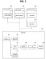
- FIG. 3 is a block diagram of an image sensing apparatus according to an embodiment of the present disclosure.
- the image sensing apparatus 30 includes a light emitter 310, a light receiver 320, a housing 331, a diffuser 332, a transparent electrode 333, a driver 340, and a substrate 400.
- the light emitter 310 may be disposed on the substrate 400 and may generate the first optical signal EL and emit the first optical signal EL to an object.
- the light emitter 310 includes a light source 311.
- the light source 311 may generate and output the first optical signal EL.
- the first optical signal EL output from the light source 311 may be infrared light with a wavelength of 770 nm to 3000 nm.
- the first optical signal EL output from the light source 311 may be visible light with a wavelength of 380 nm to 770 nm.
- the present disclosure is not limited thereto, and the light source 311 may generate a plurality of first optical signals EL with different frequencies, and may sequentially and repeatedly generate the plurality of first optical signals EL with different frequencies. Additionally, the light source 311 may simultaneously generate the plurality of first optical signals EL with different frequencies.
- the light source 311 may generate and output the first optical signal EL in the form of a pulse wave or a continuous wave.
- the continuous wave may be in the form of a sinusoid wave or a square wave.
- the light source 311 emits the generated first optical signal EL to the object for a certain integration time.
- the integration time is 1/20 [sec].
- the light source 311 may include various elements that generate and output the first optical signal EL.
- the light source 311 may include a light emitting diode (LED) or a vertical light emitting diode (VCSEL).
- the light source 311 may include a plurality of light emitting diodes arranged according to a certain pattern.
- the present disclosure is not limited thereto, and the light source 311 may include an organic light emitting diode (OLED) or a laser diode (LD).
- the light receiver 320 is located adjacent to the light emitter 310 on the substrate 400, receives the second optical signal RL emitted from the light emitter 310 and reflected from the object, and converts the received second optical signal RL into an electrical signal.
- the light receiver 320 may be arranged in the same direction as the light emitter 310, and thus reception efficiency of the second optical signal RL may be improved.
- the light receiver 320 includes a pixel array 321 that receives the second optical signal RL and converts the second optical signal RL into an electrical signal.
- the pixel array 321 may be formed inside or above the substrate 400. Although not shown, the pixel array 321 may include a plurality of pixels, and the plurality of pixels of the pixel array 321 may be arranged in a matrix form. However, the present disclosure is not limited thereto, this is just one example, and the number of pixels constituting the pixel array 321 and the arrangement of the pixels may be changed in various ways.
- Each pixel of the pixel array 321 may detect light of a wavelength corresponding to the wavelength of light output from the light emitter 310.
- each pixel in the pixel array 321 may detect infrared light.
- each pixel of the pixel array 321 may detect visible light.
- the present disclosure is not limited thereto, and the pixel array 321 may detect the second optical signal RL of various wavelengths.
- the pixel array 321 may receive the second optical signal RL during an integration time and generate an electrical signal therefor. To this end, the pixel array 321 includes a plurality of pixels. The pixel array 321 may detect the second optical signal RL reflected from an object and output pixel signals. In detail, each pixel of the pixel array 321 may generate, store, transmit, or remove charges based on control signals provided from a low driver 343, and convert the second optical signal RL, which is reflected from the object and input, into a pixel signal that is an electrical signal.
- the housing 331 may be combined with the substrate 400 on which the light emitter 310 and the light receiver 320 are mounted, and may surround the light emitter 310 and the light receiver 320 together with the substrate 400.
- the housing 331 may include an optical path hole 331a in an optical path through which the first optical signal EL emitted from the light emitter 310 is emitted to the object and the second optical signal RL reflected from the object is incident on the light receiver 320.
- the housing 331 may further include a structure for efficiently emitting the first optical signal EL emitted from the light emitter 310 and efficiently receiving the second optical signal RL reflected from an object at the light receiver 320.
- the housing 331 may further include a fixing member for optical axis alignment or an elastic member for moving an optical axis.
- the housing 331 may further include a fastening structure to effectively protect and shield the light emitter 310, the light receiver 320, and the driver 340.
- the housing 331 may further include a fastening structure such as a screw and a bolt structure or a clamp structure to be effectively fastened to the substrate 400.
- the diffuser 332 may diffuse the first optical signal EL emitted from the light emitter 310 to a Field of View (FoV) area and detect objects located within the FoV area to be detected. Because the diffuser 332 diffuses the first optical signal EL, the first optical signal EL emitted from the light emitter 310 may not be directly incident on the human eye.
- FoV Field of View
- the diffuser 332 may be located in the optical path hole 331a of the housing 331 and may be placed on the optical path of the first optical signal EL emitted from the light emitter 310 and the second optical signal RL received by the light receiver 320.
- the first optical signal EL emitted from the light source 311 may be incident on the object through the diffuser 332.
- FIG. 4 is a plan view of a transparent electrode according to an embodiment of the present disclosure.
- the transparent electrode 333 may be disposed on the diffuser 332 in the form of a mesh extending in a first direction D1 and a second direction D2.
- the present disclosure is not limited thereto, and the transparent electrode 333 may be formed in various forms that determines damage, cracks, or separation of the diffuser 332.
- the transparent electrode 333 may extend in the first direction D1 or the second direction D2, or may extend in a direction at a predetermined angle with the first direction D1 or the second direction D2.
- the transparent electrode 333 may be formed to cover a front surface of the diffuser 332.
- the transparent electrode 333 may be made of a transparent electrode material such that the first optical signal EL is emitted from the light emitter 310 to the object and the second optical signal RL reflected from the object is received by the light receiver 320.
- the transparent electrode 333 is made of indium tin oxide (ITO), indium zinc oxide (IZO), zinc oxide (ZnO), indium zinc tin oxide (IZTO), cadmium tin oxide (CTO), poly(3,4-ethylenedioxythiophene) (PEDOT), carbon nanotubes (CNT), and metal wire alone or in a mixture of two or more.
- the transparent electrode 333 may be electrically connected to the driver 340, and in particular, according to an embodiment of the present disclosure, depending on a driving mode of the image sensing apparatus 30, because the transparent electrode 333 is formed on the diffuser 332, a resistance value of the transparent electrode 333 changes and a voltage applied to the transparent electrode 333 changes in the case of damage, cracks, or separation of the diffuser 332, and thus damage, cracks, or separation of the diffuser 332 may be detected using the voltage applied to the transparent electrode 333, and the image sensing apparatus 30 may be driven to remove electromagnetic interference noise through ground by connecting the transparent electrode 333 to ground.
- the driver 340 may control the light emitter 310 to output the first optical signal EL, control the light receiver 320 to receive the second optical signal RL reflected from the object, and detect a phase difference between the first optical signal EL output from the light emitter 310 and the second optical signal RL reflected from the object and input to the light receiver to calculate pixel data.
- the driver 340 may include a timing controller 341, a light source controller 342, the low driver 343, an analog processing unit 344, an analog digital converter 345, an output buffer unit 346, and a transparent electrode driver 347, which are disposed above the substrate 400.
- the transparent electrode driver 347 may be included in a first unit circuit UC1, and the first unit circuit UC1 including the transparent electrode driver 347 may further include at least one of the timing controller 341, the light source controller 342, the low driver 343, the analog processing unit 344, the analog digital converter 345, and the output buffer unit 346.
- the first unit circuit UC1 including the transparent electrode driver 347 may include the timing controller 341, the light source controller 342, the low driver 343, the analog processing unit 344, the analog digital converter 345, the output buffer unit 346, and the transparent electrode driver 347 or may also include the timing controller 341 and the transparent electrode driver 347.
- the first unit circuit UC1 may be implemented as a single integrated circuit chip, or may be implemented as a plurality of integrated circuit chips mounted on a single printed circuit board.
- the timing controller 341 may output a signal controlling the light source 311 through the light source controller 342, and a control controlling the pixel array 321, the analog processing unit 344, the analog digital converter 345, and the output buffer unit 346 through the low driver 343, based on control of the processor 10.
- the timing controller 341 may generate a transparent electrode control signal including a first mode driving signal driving the transparent electrode 333 in a first mode M1 to check whether damage, cracks, or separation of the diffuser 332 occur and a second mode driving signal driving the transparent electrode 333 in a second mode M2 to shield electromagnetic interference noise and output the transparent electrode control signal to the transparent electrode driver 347.
- the light source controller 342 may control the light source 311 based on control of the timing controller 341.
- the light source controller 342 may modulate the first optical signal EL with a predetermined frequency and phase based on control of the processor 10 and control the light source 311 to emit the modulated first optical signal EL.
- the modulated first optical signal EL may have the form of a square wave (pulse) or a sinusoidal wave and may be infrared light, microwave, light wave, or ultrasonic wave.
- the light source controller 342 may initialize the light source 311 and adjust the int intensity of the light source 311 to be turned on or may output an optical source initialization signal to the light emitter 310 to initialize the light source 311 by adjusting an optical axis of the light source 311.
- FIG. 3 shows the case in which the light source controller 342 is included in the driver 340, but the present disclosure is not limited thereto, and the light source controller 342 may constitute the light emitter 310 together with the light source 311.
- the low driver 343 may generate signals for controlling pixels based on control of the timing controller 341 and transmit the signals to the pixels. Specifically, the low driver 343 may generate control signals for selecting and driving a row of the pixel array 321, and for example, the low driver 343 may generate a selection signal, a reset signal, and a transmission signal and transmit the generated signals to pixels corresponding to the selected row.
- the low driver 343 may initialize the pixel array 321 of the light receiver 320 together when initializing the light source 311 of the light emitter 310.
- the analog processing unit 344 may receive, sample, and hold a pixel signal output from each pixel constituting the pixel array 321.
- the analog processing unit 344 may be connected to each pixel of the pixel array 321 and may perform a correlated double sampling (CDS) operation on a pixel signal and remove noise included in the pixel signal.
- CDS correlated double sampling
- the analog digital converter 345 may convert pixel signals processed by the analog processing unit 344 into pixel data that is a digital signal.
- the analog digital converter 345 may provide the pixel data to the output buffer unit 346.
- FIG. 3 shows the case in which the analog processing unit 344 and the analog digital converter 345 are independent components, the analog digital converter 345 may be included in the analog processing unit 344 or integrated thereinto, according to another embodiment.
- the output buffer unit 346 may store pixel data transmitted from the analog digital converter 345.
- the output buffer unit 346 may output the stored pixel data to the processor 10.
- FIG. 3 shows the case in which the low driver 343, the analog processing unit 344, the analog digital converter 345, and the output buffer unit 346 are included in the driver 340, the present disclosure is not limited thereto, and at least one of the low driver 343, the analog processing unit 344, the analog digital converter 345, and the output buffer unit 346 may constitute the light receiver 320 with the pixel array 321.
- a transparent electrode control signal including a first mode driving signal driving the transparent electrode 333 in a first mode and the second mode driving signal driving the transparent electrode 333 in a second mode to shield electromagnetic interference noise may be generated and output to the transparent electrode driver 347.
- the transparent electrode driver 347 drives the transparent electrode 333 according to a mode of the image sensing apparatus 30 to detect whether damage, cracks, and separation of the diffuser 332 occur or shield electromagnetic interference noise.
- the transparent electrode driver 347 may be driven in the first mode M1 to check whether damage, cracks, or separation of the diffuser 332 occur in an initialization stage of the light source 311 and may drive the transparent electrode 333 according to the first mode driving signal received from the timing controller 341, and when determining that damage, cracks, or separation of the diffuser 332 do not occur, the transparent electrode driver 347 may be driven in the second mode M2 and may drive the transparent electrode 333 according to the second mode driving signal received from the timing controller 341 to shield electromagnetic interference noise.
- the light emitter 310 and the light receiver 320 may be driven to emit the first optical signal EL and receive the second optical signal RL reflected from the object.
- the transparent electrode driver 347 may be driven in the second mode M2.
- FIG. 5 is a circuit diagram of a transparent electrode driver according to an embodiment of the present disclosure.
- FIG. 6A is a circuit diagram showing a state in which a transparent electrode driver is driven in a first mode according to an embodiment of the present disclosure.
- FIG. 6B is a circuit diagram showing a state in which a transparent electrode driver is driven in a second mode according to an embodiment of the present disclosure.
- the transparent electrode driver 347 may include a control circuit 347a, a mode switch 347b, a voltage comparison circuit 347c, and a ground line 347d.
- the transparent electrode driver 347 may be connected to the transparent electrode 333 located above the diffuser 332 through a transparent electrode pin ITO pin of the first unit circuit UC1, and the first unit circuit UC1 may be connected to ground through a ground pin GND pin of the first unit circuit UC1.
- the control circuit 347a operates the transparent electrode driver 347 in either the first mode M1 or the second mode M2.
- the control circuit 347a may control the mode switch 347b according to a transparent electrode control signal output from the timing controller 341 and an output signal of the voltage comparison circuit 347c to operate the transparent electrode driver 347 in any one of the first mode M1 and the second mode M2.
- the control circuit 347a When receiving the first mode driving signal output from the timing controller 341, the control circuit 347a operates the transparent electrode driver 347 in the first mode M1.
- the control circuit 347a may transmit a voltage comparison circuit connection signal to the mode switch 347b, and the mode switch 347b may be driven to electrically connect the transparent electrode 333 to the voltage comparison circuit 347c.
- a voltage applied to the transparent electrode 333 and a reference voltage VREF are compared with each other by the voltage comparison circuit 347c, and the control circuit 347a receives the comparison result and determines whether the diffuser 332 is damaged.
- the timing controller 341 may receive the comparison result and may also determine whether the diffuser 332 is damaged.
- the control circuit 347a may operate the transparent electrode driver 347 in the second mode M2 according to the output signal output from the voltage comparison circuit 347c.
- the transparent electrode driver 347 may be driven to operate in the second mode M2.
- the timing controller 341 receives the output signal output from the voltage comparison circuit 347c through the control circuit 347a and determines whether the diffuser 332 is damaged, if the timing controller 341 determines that the diffuser 332 is not damaged and output the second mode driving signal to the control circuit 347a, the transparent electrode driver 347 may be driven to operate in the second mode M2.
- the control circuit 347a may transmit a ground line connection signal to the mode switch 347b, and thus, the mode switch 347b may electrically connect the transparent electrode 333 to the ground line 347d.
- the control circuit 347a When a voltage V333 applied to the transparent electrode 333 is smaller than the reference voltage VREF and it is determined that the diffuser 332 is not damaged, the control circuit 347a may be driven in the second mode M2 and may output the ground line connection signal to the mode switch 347b to connect the transparent electrode 333 to the ground line 347d, as shown in FIG. 6B .
- the control circuit 347a When the voltage V333 applied to the transparent electrode 333 is larger than the reference voltage VREF and it is determined that the diffuser 332 is damaged, the control circuit 347a may be driven to stop operations of the light emitter 310 and the light receiver 320.
- the timing controller 341 may receive a drive stop signal from the control circuit 347a and output a signal for stopping an operation of each of the light emitter 310 and the light receiver 320.
- the timing controller 341 may receive the comparison result from the voltage comparison circuit 347c through the control circuit 347a, determine that the diffuser is damaged, and output a signal for stopping operations of the light emitter 310 and the light receiver 320 to the light source controller 342, and accordingly, each of the light emitter 310 and the light receiver 320 may receive the drive stop signal from the control circuit 347a and stop operating.
- the mode switch 347b may connect the transparent electrode 333 to the voltage comparison circuit 347c or the ground line 347d depending on a mode according to a switch control signal including the voltage comparison circuit connection signal and ground line connection signal received from the control circuit 347a.
- the mode switch 347b may receive the voltage comparison circuit connection signal in the first mode M1 and may electrically connect the transparent electrode 333 to the voltage comparison circuit 347c
- the mode switch 347b may receive the ground line connection signal in the second mode M2 and may electrically connect the transparent electrode 333 to the ground line 347d.
- the transparent electrode 333 may be connected to the mode switch 347b to the voltage comparison circuit 347c through the transparent electrode pin ITO pin of the first unit circuit UC1 including the transparent electrode driver 347.
- the ground line 347d may be connected to the external ground of the first unit circuit UC1 including the transparent electrode driver 347 through a ground pin GND pin of the first unit circuit UC1 including the transparent electrode driver 347.
- the voltage comparison circuit 347c may be connected to the transparent electrode 333 through the mode switch 347b in the first mode M1, may receive and compare the reference voltage VREF and the voltage V333 applied to the transparent electrode 333, and may output the comparison result.
- the voltage comparison circuit 347c may include a first resistor R1 and a comparer CMP.
- the first resistor R1 may be connected to an input and output power voltage VDDIO and the transparent electrode 333 in the first mode M1.
- a first terminal of the first resistor R1 is connected to the input and output power voltage VDDIO, and a second terminal is connected to the transparent electrode 333 through the mode switch 347b and the transparent electrode pin ITO pin.
- the input and output power voltage VDDIO is distributed and applied to the first resistor R1 and the transparent electrode 333.
- the comparer CMP may compare the reference voltage VREF with the voltage V333 applied to the transparent electrode 333 and output the comparison result to the control circuit 347a.
- the comparer CMP receives the reference voltage VREF through a first input terminal "-”, receives the voltage V333 applied to the transparent electrode 333 through a second input terminal "+”, compare the reference voltage VREF with the voltage V333 applied to a transparent electrode, and output the comparison result to the control circuit 347a.
- the ground line 347d may be a wire connected to the ground, and may be connected to external ground of the first unit circuit UC 1 including the transparent electrode driver 347 through the ground pin GND pin of the first unit circuit UC1 including the transparent electrode driver 347. As shown in FIG. 6B , in the second mode M2, the ground line 347d may be electrically connected to the transparent electrode 333 through the transparent electrode pin ITO pin of the first unit circuit UC1 to emit electromagnetic interference noise to ground through the transparent electrode 333.
- the processor 10 may control the image sensing apparatus 30.
- the processor 10 may control the light emitter 310 to output the first optical signal EL with a predetermined frequency and a predetermined phase and may control the light receiver 320 to detect the second optical signal RL reflected from an object and generate pixel data.
- the processor 10 may calculate a distance (e.g., ToF value) between the image sensing apparatus 30 and an object, a shape of the object, a moving speed, and the like based on pixel data generated using the frequency and phase of the first optical signal EL output from the light emitter 310 and the frequency and phase of the second optical signal RL input to the light receiver 320.
- a distance e.g., ToF value
- the processor 10 may calculate a phase difference between the first optical signal EL output from the light emitter 310 based on the pixel data generated by the image sensing apparatus 30 and the second optical signal RL reflected from the object and input to the light receiver 320 and may calculate a delay time of the second optical signal RL reflected from the object and input to the light receiver 320 compared to the first optical signal EL output from the light emitter 310 using the calculated phase difference.
- the processor 10 may include an image signal processor (ISP) (not shown) for processing pixel data transmitted from the image sensing apparatus 30.
- ISP image signal processor
- the processor 10 may also be referred to as a host, a sensor controller, or the like.
- the processor 10 may be implemented separately from the image sensing apparatus 30.
- the present disclosure is not limited thereto, and the processor 10 may be integrated with the image sensing apparatus 30 and implemented as a single integrated circuit chip.
- the memory 20 may receive pixel data output from the image sensing apparatus 30 and store the pixel data. To this end, the memory 20 may include a volatile and/or non-volatile memory.
- the memory 20 may store commands or data related to at least one other component of the electronic apparatus 1.
- the memory 20 may store software and/or a program.
- the program may include, for example, a kernel, middleware, an application programming interface (API), and/or an application program. At least part of the kernel, middleware, and API may be referred to as an operation system (OS).
- OS operation system
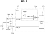
- FIG. 7 is a circuit diagram of a transparent electrode driver according to another embodiment of the present disclosure.
- the first unit circuit UC1 may include a control circuit 347a and the voltage comparison circuit 347c, and a second unit circuit UC2 may include a ground line 347d and a mode switch 348c.
- the first unit circuit UC1 may include at least one of the timing controller 341, the light source controller 342, the low driver 343, the analog processing unit 344, the analog digital converter 345, and the output buffer unit 346.
- the first unit circuit UC1 and the second unit circuit UC2 may each be implemented with one integrated circuit chip, or may be implemented with a plurality of integrated circuit chips mounted on one printed circuit board.
- the first unit circuit UC1 including the transparent electrode driver 347 may further include the transparent electrode pin ITO pin and a switching pin SW pin, the voltage comparison circuit 347c included in the first unit circuit UC1 may be electrically connected to a mode switch 348b included in the second unit circuit UC2 through the transparent electrode pin ITO pin of the first unit circuit UC1, and the control circuit 347a included in the first unit circuit UC1 may be electrically connected to the mode switch 348b included in the second unit circuit UC2 through the switching pin SW pin.
- FIG. 8 is a flowchart of driving of a light source and a transparent electrode driver according to an embodiment of the present disclosure.
- the transparent electrode driver 347 may be driven in the first mode M1 to check whether damage, cracks, or separation of the diffuser 332 occur using the transparent electrode 333, and when determining that damage, cracks, or separation of the diffuser 332 do not occur, the transparent electrode driver 347 may be driven in the second mode M2 to connect the transparent electrode 333 to ground and to shield electromagnetic interference noise, and then may drive the light emitter 310 and the light receiver 320.
- the timing controller 341 initializes the light emitter 310 and the light receiver 320 (S801).
- the timing controller 341 may control the light source controller 342 to initialize the light source 311 of the light emitter 310 and initialize the pixel array 321 of the light receiver 320.
- the timing controller 341 may control the light source controller 342, and the light source controller 342 may adjust the intensity of the light source 311 to be turned on or may initialize the light emitter 310 and the light receiver 320 by adjusting an optical axis to efficiently emit the first optical signal EL from the light emitter 310 toward an object and to efficiently receive the second optical signal RL reflected from the object by the light receiver 320.
- the transparent electrode driver 347 is driven in the first mode M1 to detect whether the diffuser 332 is damaged (S802).
- the voltage comparison circuit 347c and the transparent electrode 333 are connected to each other by the mode switch 347b that receives the voltage comparison circuit connection signal from the control circuit 347a, and the input and output power voltage VDDIO is applied to the transparent electrode 333 and the first resistor R1.
- the input and output power voltage VDDIO is distributed and applied to the first resistor R1 and the transparent electrode 333, the voltage V333 applied to the transparent electrode 333 is input to the comparer CMP through the second input terminal "+”, and the reference voltage VREF is input to the comparer CMP through the first input terminal "-”.
- the comparer CMP compares the reference voltage VREF input through the first input terminal "-” with the voltage V333 applied to the transparent electrode 333, input through the second input terminal "+”, and outputs the comparison result to the control circuit 347a.
- the control circuit 347a may receive the result obtained by comparing the reference voltage VREF with the voltage V333 applied to the transparent electrode 333, from the voltage comparison circuit 347c, determine whether the diffuser 332 is damaged, and drive the transparent electrode driver 347 to operate in the second mode or drive the light emitter 310 and the light receiver 320 to stop operating according to whether the diffuser 332 is damaged.
- the timing controller 341 receives an output signal output from the voltage comparison circuit 347c through the control circuit 347a and determines whether the diffuser 332 is damaged, and when the timing controller 341 determines that the diffuser 332 is not damaged and outputs the second mode driving signal to the control circuit 347a, the transparent electrode driver 347 may be driven to operate in the second mode M2.
- the control circuit 347a When the voltage V333 applied to the transparent electrode 333 is smaller than the reference voltage VREF and it is determined that the diffuser 332 is not damaged, the control circuit 347a may be driven in the second mode M2 to output the ground line connection signal to the mode switch 347b to connect the transparent electrode 333 to the ground line 347d, as shown in FIG. 6B . When a voltage applied to the transparent electrode 333 is greater than the reference voltage VREF and it is determined that the diffuser 332 is damaged, the control circuit 347a may be driven to stop operations of the light emitter 310 and the light receiver 320.
- the transparent electrode driver 347 is driven in the second mode M2 to shield electromagnetic interference noise (S811).
- the ground line 347d and the transparent electrode 333 are connected by the mode switch 347b, which receives the ground line connection signal from the control circuit 347a, and electromagnetic interference noise may be removed through the transparent electrode 333 connected to the ground.
- the light emitter 310 and the light receiver 320 may be driven to operate (S812). That is, while the transparent electrode driver 347 is driven in the second mode M2 to shield electromagnetic interference noise, the light emitter 310 and the light receiver 320 may operate to perform image sensing.
- the timing controller 341 may receive a drive stop signal from the control circuit 347a and output a signal for stopping an operation to each of the light emitter 310 and the light receiver 320.
- the timing controller 341 may receive the comparison result through the control circuit 347a from the voltage comparison circuit 347c to determine that the diffuser is damaged and output a signal for stopping operations of the light emitter 310 and the light receiver 320 to the light source controller 342, and each of the light emitter 310 and the light receiver 320 may receive a drive stop signal from the control circuit 347a and stop operating.
- the image sensing apparatus may not only detect damage, cracks, and separation of the diffuser in the first mode by using a transparent electrode located on the diffuser but also shield electromagnetic interference noise caused by high-frequency driving in the second mode.
- whether damage, cracks, or separation of the diffuser occur may be determined and electromagnetic interference noise may be shielded using a transparent electrode located on the diffuser, thereby reducing the volume and weight of the image sensing apparatus.
Landscapes
- Engineering & Computer Science (AREA)
- Physics & Mathematics (AREA)
- General Physics & Mathematics (AREA)
- Computer Networks & Wireless Communication (AREA)
- Radar, Positioning & Navigation (AREA)
- Remote Sensing (AREA)
- Electromagnetism (AREA)
- Measurement Of Optical Distance (AREA)
- Geophysics And Detection Of Objects (AREA)
- Length Measuring Devices By Optical Means (AREA)
Applications Claiming Priority (2)
| Application Number | Priority Date | Filing Date | Title |
|---|---|---|---|
| KR20220119482 | 2022-09-21 | ||
| KR1020230085519A KR20240040606A (ko) | 2022-09-21 | 2023-07-03 | 이미지 센싱 장치, 이를 포함하는 전자 장치 및 이미지 센싱 장치의 구동 방법 |
Publications (2)
| Publication Number | Publication Date |
|---|---|
| EP4343373A1 true EP4343373A1 (de) | 2024-03-27 |
| EP4343373B1 EP4343373B1 (de) | 2026-01-14 |
Family
ID=88021121
Family Applications (1)
| Application Number | Title | Priority Date | Filing Date |
|---|---|---|---|
| EP23197108.6A Active EP4343373B1 (de) | 2022-09-21 | 2023-09-13 | Bilderfassungsvorrichtung, elektronische vorrichtung damit und ansteuerungsverfahren für bilderfassungsvorrichtung |
Country Status (2)
| Country | Link |
|---|---|
| US (1) | US20240094364A1 (de) |
| EP (1) | EP4343373B1 (de) |
Citations (5)
| Publication number | Priority date | Publication date | Assignee | Title |
|---|---|---|---|---|
| US20120075214A1 (en) * | 2010-09-28 | 2012-03-29 | Kim Tae-Hwan | Display Device with an Embedded Touch Panel and a Method of Manufacturing the Same |
| KR20210096827A (ko) * | 2020-01-29 | 2021-08-06 | 엘지이노텍 주식회사 | 카메라 모듈 |
| US20220066036A1 (en) * | 2020-08-25 | 2022-03-03 | Lumentum Operations Llc | Package for a time of flight device |
| KR20220119482A (ko) | 2019-12-30 | 2022-08-29 | 광동 메이디 컨슈머 일렉트릭스 매뉴팩쳐링 컴퍼니 리미티드 | 식품 가공기 및 이의 칼세트 장착구조와 믹싱컵 |
| KR20230085519A (ko) | 2021-12-07 | 2023-06-14 | 엘지디스플레이 주식회사 | 발광표시장치 및 이의 제조방법 |
Family Cites Families (1)
| Publication number | Priority date | Publication date | Assignee | Title |
|---|---|---|---|---|
| KR102655932B1 (ko) * | 2019-04-03 | 2024-04-11 | 삼성전자주식회사 | 전자 장치 및 전자 장치의 광원 출력 제어방법 |
-
2023
- 2023-09-13 EP EP23197108.6A patent/EP4343373B1/de active Active
- 2023-09-20 US US18/471,148 patent/US20240094364A1/en active Pending
Patent Citations (5)
| Publication number | Priority date | Publication date | Assignee | Title |
|---|---|---|---|---|
| US20120075214A1 (en) * | 2010-09-28 | 2012-03-29 | Kim Tae-Hwan | Display Device with an Embedded Touch Panel and a Method of Manufacturing the Same |
| KR20220119482A (ko) | 2019-12-30 | 2022-08-29 | 광동 메이디 컨슈머 일렉트릭스 매뉴팩쳐링 컴퍼니 리미티드 | 식품 가공기 및 이의 칼세트 장착구조와 믹싱컵 |
| KR20210096827A (ko) * | 2020-01-29 | 2021-08-06 | 엘지이노텍 주식회사 | 카메라 모듈 |
| US20220066036A1 (en) * | 2020-08-25 | 2022-03-03 | Lumentum Operations Llc | Package for a time of flight device |
| KR20230085519A (ko) | 2021-12-07 | 2023-06-14 | 엘지디스플레이 주식회사 | 발광표시장치 및 이의 제조방법 |
Also Published As
| Publication number | Publication date |
|---|---|
| EP4343373B1 (de) | 2026-01-14 |
| US20240094364A1 (en) | 2024-03-21 |
Similar Documents
| Publication | Publication Date | Title |
|---|---|---|
| US11620805B2 (en) | Integrated electronic module for 3D sensing applications, and 3D scanning device including the integrated electronic module | |
| JP7290571B2 (ja) | 統合化されたlidar照明出力制御 | |
| KR102454144B1 (ko) | 동기화된 회전식 lidar 및 롤링 셔터 카메라 시스템 | |
| US9151829B2 (en) | Packaged radiation source and detector | |
| JP7113018B2 (ja) | 乗物センサの可変ビーム間隔、タイミング、およびパワー | |
| US20210041534A1 (en) | Distance measurement module, distance measurement method, and electronic apparatus | |
| CN112055820B (zh) | 利用不同发射场的飞行时间测距 | |
| US11808890B2 (en) | Distance measuring device and method of measuring distance by using the same | |
| CN108072879A (zh) | 一种光学测距的方法及装置 | |
| KR20220000664U (ko) | 미광 안내-제거 구조를 갖는 tof 광학 센싱 모듈 | |
| EP4343373A1 (de) | Bilderfassungsvorrichtung, elektronische vorrichtung damit und ansteuerungsverfahren für bilderfassungsvorrichtung | |
| EP3470872B1 (de) | Sensorvorrichtung | |
| WO2022002974A1 (en) | Window and mirror presence detection system and corresponding method | |
| US20220413107A1 (en) | Distance measurement apparatus and distance measurement system | |
| KR20240040606A (ko) | 이미지 센싱 장치, 이를 포함하는 전자 장치 및 이미지 센싱 장치의 구동 방법 | |
| CN117747626A (zh) | 图像感测设备、包括其的电子设备及其驱动方法 | |
| CN113126111B (zh) | 飞行时间模组和电子设备 | |
| KR20200114164A (ko) | 카메라 모듈형 센서 장치 및 카메라 모듈 | |
| CN115480262A (zh) | 测距装置、激光雷达和移动机器人 | |
| CN112153184B (zh) | 移动终端 | |
| US20250076465A1 (en) | Retroreflective mechanisms on optical ranging, proximity, and image sensors to reduce optical noise from unwanted sources | |
| US20150241989A1 (en) | Off-axis detection for proximity or gesture sensor | |
| EP3962065B1 (de) | Kameramodul | |
| US20050237302A1 (en) | Optical mouse capable of increasing voltage to a predetermined voltage level and measuring movement with respect to a surface | |
| US20200217932A1 (en) | Ladar packaging for vehicle range sensors |
Legal Events
| Date | Code | Title | Description |
|---|---|---|---|
| PUAI | Public reference made under article 153(3) epc to a published international application that has entered the european phase |
Free format text: ORIGINAL CODE: 0009012 |
|
| STAA | Information on the status of an ep patent application or granted ep patent |
Free format text: STATUS: THE APPLICATION HAS BEEN PUBLISHED |
|
| AK | Designated contracting states |
Kind code of ref document: A1 Designated state(s): AL AT BE BG CH CY CZ DE DK EE ES FI FR GB GR HR HU IE IS IT LI LT LU LV MC ME MK MT NL NO PL PT RO RS SE SI SK SM TR |
|
| STAA | Information on the status of an ep patent application or granted ep patent |
Free format text: STATUS: REQUEST FOR EXAMINATION WAS MADE |
|
| 17P | Request for examination filed |
Effective date: 20240927 |
|
| RBV | Designated contracting states (corrected) |
Designated state(s): AL AT BE BG CH CY CZ DE DK EE ES FI FR GB GR HR HU IE IS IT LI LT LU LV MC ME MK MT NL NO PL PT RO RS SE SI SK SM TR |
|
| P01 | Opt-out of the competence of the unified patent court (upc) registered |
Free format text: CASE NUMBER: APP_62386/2024 Effective date: 20241122 |
|
| GRAP | Despatch of communication of intention to grant a patent |
Free format text: ORIGINAL CODE: EPIDOSNIGR1 |
|
| STAA | Information on the status of an ep patent application or granted ep patent |
Free format text: STATUS: GRANT OF PATENT IS INTENDED |
|
| RIC1 | Information provided on ipc code assigned before grant |
Ipc: G01S 7/481 20060101AFI20250722BHEP Ipc: G01S 7/487 20060101ALI20250722BHEP Ipc: G01S 7/497 20060101ALI20250722BHEP Ipc: G01S 17/894 20200101ALI20250722BHEP |
|
| INTG | Intention to grant announced |
Effective date: 20250808 |
|
| GRAS | Grant fee paid |
Free format text: ORIGINAL CODE: EPIDOSNIGR3 |
|
| GRAA | (expected) grant |
Free format text: ORIGINAL CODE: 0009210 |
|
| STAA | Information on the status of an ep patent application or granted ep patent |
Free format text: STATUS: THE PATENT HAS BEEN GRANTED |
|
| AK | Designated contracting states |
Kind code of ref document: B1 Designated state(s): AL AT BE BG CH CY CZ DE DK EE ES FI FR GB GR HR HU IE IS IT LI LT LU LV MC ME MK MT NL NO PL PT RO RS SE SI SK SM TR |
|
| REG | Reference to a national code |
Ref country code: CH Ref legal event code: F10 Free format text: ST27 STATUS EVENT CODE: U-0-0-F10-F00 (AS PROVIDED BY THE NATIONAL OFFICE) Effective date: 20260114 Ref country code: GB Ref legal event code: FG4D |
|
| REG | Reference to a national code |
Ref country code: DE Ref legal event code: R096 Ref document number: 602023010680 Country of ref document: DE |
|
| REG | Reference to a national code |
Ref country code: IE Ref legal event code: FG4D |