EP4343393A1 - Guide d'ondes optique diffractif et appareil d'affichage le comprenant - Google Patents
Guide d'ondes optique diffractif et appareil d'affichage le comprenant Download PDFInfo
- Publication number
- EP4343393A1 EP4343393A1 EP23188917.1A EP23188917A EP4343393A1 EP 4343393 A1 EP4343393 A1 EP 4343393A1 EP 23188917 A EP23188917 A EP 23188917A EP 4343393 A1 EP4343393 A1 EP 4343393A1
- Authority
- EP
- European Patent Office
- Prior art keywords
- vertex
- grating
- straight line
- diffractive optical
- optical waveguide
- Prior art date
- Legal status (The legal status is an assumption and is not a legal conclusion. Google has not performed a legal analysis and makes no representation as to the accuracy of the status listed.)
- Granted
Links
Images





Classifications
-
- G—PHYSICS
- G02—OPTICS
- G02B—OPTICAL ELEMENTS, SYSTEMS OR APPARATUS
- G02B27/00—Optical systems or apparatus not provided for by any of the groups G02B1/00 - G02B26/00, G02B30/00
- G02B27/42—Diffraction optics, i.e. systems including a diffractive element being designed for providing a diffractive effect
- G02B27/4205—Diffraction optics, i.e. systems including a diffractive element being designed for providing a diffractive effect having a diffractive optical element [DOE] contributing to image formation, e.g. whereby modulation transfer function MTF or optical aberrations are relevant
-
- G—PHYSICS
- G02—OPTICS
- G02B—OPTICAL ELEMENTS, SYSTEMS OR APPARATUS
- G02B6/00—Light guides; Structural details of arrangements comprising light guides and other optical elements, e.g. couplings
- G02B6/0001—Light guides; Structural details of arrangements comprising light guides and other optical elements, e.g. couplings specially adapted for lighting devices or systems
- G02B6/0011—Light guides; Structural details of arrangements comprising light guides and other optical elements, e.g. couplings specially adapted for lighting devices or systems the light guides being planar or of plate-like form
- G02B6/0033—Means for improving the coupling-out of light from the light guide
- G02B6/005—Means for improving the coupling-out of light from the light guide provided by one optical element, or plurality thereof, placed on the light output side of the light guide
-
- G—PHYSICS
- G02—OPTICS
- G02B—OPTICAL ELEMENTS, SYSTEMS OR APPARATUS
- G02B27/00—Optical systems or apparatus not provided for by any of the groups G02B1/00 - G02B26/00, G02B30/00
- G02B27/0081—Optical systems or apparatus not provided for by any of the groups G02B1/00 - G02B26/00, G02B30/00 with means for altering, e.g. enlarging, the entrance or exit pupil
-
- G—PHYSICS
- G02—OPTICS
- G02B—OPTICAL ELEMENTS, SYSTEMS OR APPARATUS
- G02B27/00—Optical systems or apparatus not provided for by any of the groups G02B1/00 - G02B26/00, G02B30/00
- G02B27/01—Head-up displays
- G02B27/017—Head mounted
- G02B27/0172—Head mounted characterised by optical features
-
- G—PHYSICS
- G02—OPTICS
- G02B—OPTICAL ELEMENTS, SYSTEMS OR APPARATUS
- G02B5/00—Optical elements other than lenses
- G02B5/18—Diffraction gratings
-
- G—PHYSICS
- G02—OPTICS
- G02B—OPTICAL ELEMENTS, SYSTEMS OR APPARATUS
- G02B5/00—Optical elements other than lenses
- G02B5/18—Diffraction gratings
- G02B5/1814—Diffraction gratings structurally combined with one or more further optical elements, e.g. lenses, mirrors, prisms or other diffraction gratings
- G02B5/1819—Plural gratings positioned on the same surface, e.g. array of gratings
-
- G—PHYSICS
- G02—OPTICS
- G02B—OPTICAL ELEMENTS, SYSTEMS OR APPARATUS
- G02B5/00—Optical elements other than lenses
- G02B5/18—Diffraction gratings
- G02B5/1842—Gratings for image generation
-
- G—PHYSICS
- G02—OPTICS
- G02B—OPTICAL ELEMENTS, SYSTEMS OR APPARATUS
- G02B6/00—Light guides; Structural details of arrangements comprising light guides and other optical elements, e.g. couplings
- G02B6/24—Coupling light guides
- G02B6/26—Optical coupling means
- G02B6/34—Optical coupling means utilising prism or grating
-
- G—PHYSICS
- G02—OPTICS
- G02B—OPTICAL ELEMENTS, SYSTEMS OR APPARATUS
- G02B27/00—Optical systems or apparatus not provided for by any of the groups G02B1/00 - G02B26/00, G02B30/00
- G02B27/01—Head-up displays
- G02B27/0101—Head-up displays characterised by optical features
- G02B2027/0123—Head-up displays characterised by optical features comprising devices increasing the field of view
- G02B2027/0125—Field-of-view increase by wavefront division
-
- G—PHYSICS
- G02—OPTICS
- G02B—OPTICAL ELEMENTS, SYSTEMS OR APPARATUS
- G02B27/00—Optical systems or apparatus not provided for by any of the groups G02B1/00 - G02B26/00, G02B30/00
- G02B27/01—Head-up displays
- G02B27/017—Head mounted
- G02B2027/0178—Eyeglass type
-
- G—PHYSICS
- G02—OPTICS
- G02B—OPTICAL ELEMENTS, SYSTEMS OR APPARATUS
- G02B6/00—Light guides; Structural details of arrangements comprising light guides and other optical elements, e.g. couplings
- G02B6/10—Light guides; Structural details of arrangements comprising light guides and other optical elements, e.g. couplings of the optical waveguide type
- G02B6/12—Light guides; Structural details of arrangements comprising light guides and other optical elements, e.g. couplings of the optical waveguide type of the integrated circuit kind
- G02B6/122—Basic optical elements, e.g. light-guiding paths
- G02B6/124—Geodesic lenses or integrated gratings
Definitions
- the present disclosure relates to a display technology based on diffraction, in particular to a diffractive optical waveguide and a display apparatus having the diffractive optical waveguide.
- Diffraction-based display technology has developed rapidly in recent years, and it can be applied to a display apparatus such as a near-eye display apparatus, a head-mounted display apparatus, and a head-up display apparatus.
- a diffractive optical waveguide is an important optical device that can be used in diffraction display technology.
- the diffractive optical waveguide that can be used for display is provided with a coupling-in grating and a coupling-out grating on a waveguide substrate; the coupling-in grating couples incident light carrying image information into the waveguide substrate; the coupling-out grating propagates and expands the light carrying image information, and at the same time couples the light out of the waveguide substrate to form a coupled-out light field.
- the eye receives the light of the coupled-out light field so that an image carried by the incident light can be observed.
- the coupling-out grating of the diffractive optical waveguide can adopt a two-dimensional grating structure.
- an optical unit structure usually adopts a circular, rectangular, or rhombus structure in cross-section.
- the light coupled-out efficiency as well as the uniformity of an output light field of the diffraction waveguide still needs to be improved urgently.
- the object of the present disclosure is to provide a diffractive optical waveguide, a design method and a forming method thereof, and a display apparatus including the diffractive optical waveguide, so as to at least partly overcome the deficiencies in the prior art.
- a diffractive optical waveguide including a waveguide substrate and a coupling-out grating formed on the waveguide substrate, wherein the coupling-out grating is configured to couple at least a portion of light within the waveguide substrate propagating thereinto through total internal reflection along a coupling-in direction out of the waveguide substrate by diffraction, the coupling-out grating includes a first grating, and the first grating includes a plurality of first optical unit structures arranged in an array along a plane and has a first grating vector, a second grating vector, and a third grating vector, wherein a direction of the first grating vector is a first direction, and the first direction is substantially consistent with the coupling-in direction, and directions of the second grating vector and the third grating vector, being respectively towards both sides of the first direction, form respective acute angles with the first direction, wherein:
- the third straight line and the fourth straight line are substantially perpendicular to the second grating vector or the third grating vector.
- a part of the first predetermined profile between any two adjacent vertices adjacent to each other of the first vertex, the second vertex, the third vertex, and the fourth vertex deviates from a straight line extending through the two vertices by a distance less than or equal to one-fifth of a distance between the two vertices.
- the third straight line and the fourth straight line are parallel to each other.
- the first predetermined profile has an overall length L in the first direction and an average width W in the second direction, where 0.1L ⁇ W ⁇ L.
- the first predetermined profile is a quadrilateral.
- a profile line connecting at least one pair of adjacent vertices among the first vertex, the second vertex, the third vertex, and the fourth vertex along the circumferential direction is a curve.
- a profile line connecting the first vertex and the second vertex and a profile line connecting the third and the fourth vertex are curves, and/or a profile line connecting the first vertex and the fourth vertex and a profile line connecting the second vertex and the third vertex are curves.
- the first predetermined profile further has a fifth vertex and a sixth vertex, the fifth vertex is located between the first vertex and the fourth vertex along the circumferential direction, and the sixth vertex is located between the second vertex and the third vertex along the circumferential direction.
- a distance from the fifth vertex to the first vertex is substantially equal to that from the fifth vertex to the fourth vertex, and a distance from the sixth vertex to the second vertex is substantially equal to that from the sixth vertex to the third vertex.
- a straight line extending through the first vertex and the fifth vertex and a straight line extending through the third vertex and the sixth vertex are parallel to each other, and a straight line extending through the fourth vertex and the fifth vertex and a straight line extending through the second vertex and the sixth vertex are parallel to each other; or the straight line extending through the first vertex and the fifth vertex and the straight line extending through the second vertex and the sixth vertex are parallel to each other, and the straight line extending through the fourth vertex and the fifth vertex and the straight line extending through the third vertex and the sixth vertex parallel to each other.
- a profile line, between at least one pair of adjacent vertices connected circumferentially among the first vertex, the second vertex, the third vertex, the fourth vertex, the fifth vertex, and the sixth vertex is a curve.
- profile lines, between adjacent vertices connected circumferentially among the first vertex, the second vertex, the third vertex, the fourth vertex, the fifth vertex, and the sixth vertex are curves.
- n 2.
- the coupling-out grating further includes a second grating, which includes a plurality of second optical unit structures arranged in an array along the plane, and has the first grating vector, the second grating vector, and the third grating vector;
- the coupling-out grating further includes a third grating
- the third grating includes a plurality of third optical unit structures arranged in an array along the plane and has the first grating vector, the second grating vector, and the third grating vector;
- the third optical unit structure has a third predetermined profile symmetrical with respect to an axis along the first direction when viewed in the plane; and the third grating is arranged between the first grating and the second grating along the second direction.
- the coupling-out grating further includes a fourth grating and a fifth grating, arranged side by side with the first grating and the second grating in the second direction and respectively located outside the first grating and the second grating; and the fourth grating is a one-dimensional grating and has a fourth grating vector, the fifth grating is a one-dimensional grating and has a fifth grating vector, the fourth grating vector and the fifth grating vector are respectively the same as the second grating vector and the third grating vector, the fourth grating vector faces a direction away from the fifth grating, and the fifth grating vector faces a direction away from the fourth grating.
- the coupling-out grating further includes a third grating, the third grating including a plurality of third optical unit structures arranged in an array along the plane and has the first grating vector, the second grating vector, and the third grating vector; the third optical unit structure has a third predetermined profile symmetrical with respect to an axis along the first direction when viewed in the plane; and the first grating and the third grating are arranged side by side in the second direction so that the third straight line and the fourth straight line in the first predetermined profile of the first grating tilt towards the third grating along the first direction.
- a display apparatus which includes the above-mentioned diffractive optical waveguide.
- the display apparatus is a near-eye display apparatus and includes a lens and a frame for holding the lens close to the eye, the lens including the diffractive optical waveguide.
- the display apparatus is an augmented reality display apparatus or a virtual reality display apparatus.
- the coupling-out grating at least partially adopts the first grating and/or the second grating that are left-right asymmetric with respect to the first direction (basically the direction of the first grating vector consistent with the coupling-in direction), which can greatly improve light splitting ability to one-side region.
- the first grating and/or the second grating have the structural characteristics perpendicular to the first direction, which is equivalent to truncate the one-dimensional grating, so as to obtain a stronger modulation effect of the first grating vector, enabling enhanced light beam coupled-out capability in the one-sided region.
- a diffractive optical waveguide 1 shown in Figure 1 includes a waveguide substrate 1a, and a coupling-out grating 10 and a coupling-in grating 20 arranged on the waveguide substrate 1a.
- the coupling-out grating 10 is a two-dimensional grating, which has optical unit structures A(s), arranged in an array with a hexagonal (or an equilateral triangle) manner, as shown in a dotted line box on a left side of Figure 1 .
- the optical unit structure has a rhombic cross-section in a plane parallel to the plane (x-y plane shown in Figure) of the waveguide substrate 100a.
- the two-dimensional coupling-out grating 10 has a first grating vector G1, a second grating vector G2, and a third grating vector G3, wherein the direction of the first grating vector G1 is the first direction (that is, x direction), which is also the coupling-in direction In of light propagating from the coupling-in grating 20 to the coupling-out grating 10.
- the acute angle is preferably 60°.
- the coupling-in grating 20 has the first grating vector G1.
- the light coupled into the waveguide substrate 1a through the coupling-in grating 20 can be coupled out from the waveguide substrate 1a under an action of negative first-order diffraction of the first grating vector G1 of the coupling-out grating 10, or can be coupled out from the waveguide substrate 1a under superposition of the negative first-order diffraction of the second grating vector G2 and the third grating vector G3 of the coupling-out grating 10.
- a coupling-out grating 10' of a diffractive optical waveguide 2 shown in Figure 2 is composed of one-dimensional gratings 11 and 12 respectively provided at both sides, and a two-dimensional grating 13 therebetween.
- the two-dimensional grating 13 may adopt the same structure as that of the coupling-out grating 10 shown in Figure 1 , which will not be repeated here.
- a coupling-in grating 20 in the diffractive optical waveguide 2 is the same as that in the diffractive optical waveguide 1 shown in Figure 1 , and both have the first grating vector G1, which will not be repeated here.
- Figure 3 shows examples of simulation diagrams of the light intensity distribution of the output light fields of the diffractive optical waveguide shown in Figure 1 and Figure 2 .
- a bright line in the middle appears in the output light field of the diffractive optical waveguide 1, with low brightness on both sides and poor uniformity.
- the diffractive optical waveguide 2 can suppress the bright line in the middle of the field of view, significantly increase the brightness of the fields of view at both sides, and improve the uniformity.
- the overall uniformity of the light intensity distribution of the diffractive optical waveguide 2 is still unsatisfactory, especially as indicated by the two arrows in Figure 3 , there are two obvious strip-shaped dark regions in a transition region between a middle of a field of view and an edge of the field of view.
- the present disclosure is made based on following observations and research on causes of forming strip-shaped dark regions in the light intensity distribution of the diffractive optical waveguide shown in Figure 2 .
- the light incident on the diffractive optical waveguide 2 is coupled into the waveguide substrate 2a through the positive first-order diffraction of the first grating vector G1 of the coupling-in grating 20, and propagates to the coupling-out grating 10' in the waveguide substrate by total internal reflection.
- Figure 4 schematically shows that the field angle of view FOVX formed by a normal of the x-y plane where the diffractive optical waveguide 2 is located in the direction around the x-axis substantially corresponds to a light beam H at a central angle (see Figure 3 , about -5o) of one of the strip-shaped dark regions.
- FOVX field angle of view
- Figure 4 shows that after the light beam H propagates to the one-dimensional grating 11 on the left side of the coupling-out grating 10', since the one-dimensional grating 11 only has the second grating vector G2, the light beam H cannot be coupled out of the waveguide substrate in the entire region of the one-dimensional grating 11.
- the loss of the coupled-out light beam in the region indicated by the reference number "B" in Figure 4 of the one-dimensional grating 11 results in (or spatially corresponds to) the strip-shaped dark region of the field angle of view FOVX at around -5o in the light intensity distribution of the diffractive optical waveguide 2 as shown in the graph on the right side of Figure 3 .
- the one-dimensional grating 12' is in the same or similar situation, resulting in the other strip-shaped dark region in the light intensity distribution.
- a coupling-out grating 10" of the diffractive optical waveguide 3 includes a first grating 11'and a second grating 12', and a third grating 13 therebetween, wherein the third grating 13 may have the same grating structure as the third grating 13 of the diffractive optical waveguide 2 shown in Figure 2 .
- the first grating 11' and the second grating 12' adopt two-dimensional gratings instead of one-dimensional gratings, and both have the same first grating vector G1, second grating vector G2, and third grating vector G3 as that of the third grating 13.
- the first grating 11' and the second grating 12' differ from the third grating 13 in that their grating structures enable that a modulation effect of the first grating vector G1 as well as the second grating vector G2 of the first grating 11' is very strong while the modulation effect of the third grating vector G3 is very weak, and a modulation effect of the first grating vector G1 as well as the third grating vector G3 of the second grating 12' is relatively strong, while a modulation effect of the second grating vector G2 is very weak.
- Figure 5 schematically illustrates a principle of brightness enhancement of the strip-shaped dark regions in the light intensity distribution of the diffractive optical waveguide shown in Figure 2 in a diffractive optical waveguide 3.
- the light incident on the diffractive optical waveguide 3 is coupled into a waveguide substrate 3a through the positive first-order diffraction of the first grating vector G1 of the coupling-in grating 20, and propagates to the coupling-out grating 10" in the waveguide substrate by total internal reflection.
- the modulation effect of the second grating vector G2 of the first grating 11' is significantly stronger than that of the third grating vector G3, which enables most of the light quantity in the light beam H to be split to the right side of the total reflection propagation path under the modulation effect of the second grating vector G2, and only a small amount to be split to the left side.
- the first grating 11' as having the second grating vector G2 with a strong modulation effect and the third grating vector G3 with a weak modulation effect, it is beneficial to split light towards one side of the total reflection propagation path that contributes the light quantity in the eyebox (on the right side of the total reflection propagation path in the example shown in Figure 5 ) and suppress the light splitting on the other side that makes no or little contribute to the light quantity in the eyebox, so as to avoid the light the loss of light quantity, and improve the overall light coupling-out efficiency.
- the efficiency of coupling the light out of the waveguide substrate can be effectively improved on the side where the amount of split light is large in the region of the first grating 11', including increasing the efficiency of coupling the light out of a region B, thus increasing the light quantity in the area of the field of view of diffractive optical waveguide 3,which corresponds to the corresponding strip-shaped dark region of the diffractive optical waveguide 2, and thus improving the uniformity of the output light field.
- the second grating 12' in the coupling-out grating 10" of the diffractive optical waveguide 3 is in the same or similar situation as that of the first grating 11', so that it is beneficial to increase the light quantity in another strip-shaped dark region. It should be understood that in some implementations, the coupling-out grating 10" of the diffractive optical waveguide 3 may not include the second grating 12'.
- a new diffractive optical waveguide wherein the modulation effect of the first grating vector G1 is enhanced by optimizing a cross-section profile of at least a part of the optical unit structures of the coupling-out grating, and the modulation effect of one of the second grating vector G2 and the third grating vector G3 is enhanced while suppressing that of the other one of them, so as to form an asymmetry with respect to the direction (first direction) of the first grating vector G1.
- Such a coupling-out grating is capable of forming an enhanced single-side light splitting and enhancing the coupling of the light out of this side, which is beneficial to improve the uniformity of the output light field of the diffractive optical waveguide, and at the same time reduces the loss of the light quantity/coupled-out efficiency within an eyebox range caused by the increasing of the light being coupled out.
- the optimized cross-section profile (that is, the profile observed in the x-y plane) of at least a part of the optical unit structures of the coupling-out grating has a first vertex C1, a second vertex C2, a third vertex C3, and a fourth vertex C4.
- the first vertex C1 and the second vertex C2 are located at one end of the profile in an x direction
- the third vertex C3 and the fourth vertex C4 are located at the other end of the profile in the x direction
- the first vertex C1 and the third vertex C3 are outermost vertices of the profile in the y direction.
- a first straight line l1 extending through the first vertex C1 and the second vertex C2 and a second straight line l2 extending through the third vertex C3 and the fourth vertex C4 are perpendicular to the x direction
- “same positive or negative sign” means that the third straight line l3 and the fourth straight line l4 are inclined to a same side with respect to the x direction.
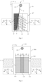
- FIG 6 is a schematic diagram of a diffractive optical waveguide 100 according to Embodiment 1 of the present disclosure.
- the diffractive optical waveguide 100 includes a waveguide substrate 100a, and a coupling-out grating 110 and a coupling-in grating 120 formed on the waveguide substrate 100a.
- the coupling-out grating 110 is configured to couple at least a portion of light within the waveguide substrate 100a propagating thereinto through total internal reflection substantially along a coupling-in direction out of the waveguide substrate 100a by diffraction.
- the coupling-out grating 110 includes a first grating 111, a second grating 112, and a third grating 113, the third grating 113 being located between the first grating 111 and the second grating 112 along the y direction perpendicular to the x direction, the first grating 111, the second grating 112, and the third grating 113 having the same first grating vector G1, second grating vector G2, and third grating vector G3.
- the direction of the first grating vector G1 is the first direction (that is, the x direction), which is also the coupling-in direction of the light propagating to the coupling-out grating 110.
- Each of the first grating 111, the second grating 112, and the third grating 113 includes a plurality of optical unit structures arranged in an array along the x-y plane.
- the third grating 113 may have a common grating structure for a two-dimensional coupling-out grating.
- its optical unit structure can have a symmetrical profile relative to the x-axis when viewed in the x-y plane, such as a rhombus as shown in Figure 1 , or it can be, for example, a circle, rectangle or any other suitable shape.
- the first grating 111 and the second grating 112 include the optical unit structures having the optimized cross-section profiles described above according to the present disclosure.
- the optical unit structure of the second grating 112 and the optical unit structure of the first grating 111 may be symmetrical or approximately symmetrical to each other with respect to the x-axis.
- the first grating 111 will be described in detail below as an example.
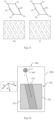
- Figure 7 shows an enlarged view of the first grating 111 of the coupling-out grating 110 of the diffractive optical waveguide 100.
- Figure 8 is an enlarged view of the profile of the optical unit structure U of the first grating 111 viewed in the x-y plane.
- the profile of the optical unit structure U of the first grating 111 is a parallelogram shape, wherein the profile lines connected between the respective vertices C1, C2, C3, and C4 are straight lines and opposite sides are parallel to each other, especially the profile line connected between the first vertex C1 and the second vertex C2 (coincident with the first straight line 11) and the profile line connected between the third vertex C3 and the fourth vertex C4 (coincident with the second straight line l2) are perpendicular to the x direction.
- the profile line connected between the first vertex C1 and the fourth vertex C4 (coincident with the third straight line l3) and the profile line connected between the second vertex C2 and the third vertex C3 (coinciding with the fourth straight line l4) are substantially perpendicular to the direction of the second grating vector G2.
- the second grating vector G2 is inclined at an angle of 60° to one side with respect to the x direction
- the above profile line is inclined at an angle of 30° to the other side with respect to the x direction.
- the second grating 112 includes the optical unit structure having an optimized cross-section profile described above according to the present disclosure.
- the profile of the optical unit structure of the second grating 112 has a seventh vertex, an eighth vertex, a ninth vertex, and a tenth vertex arranged in sequence along the circumferential direction, wherein the seventh vertex and the eighth vertex are located at one end of the profile in the x direction, the ninth vertex and the tenth vertex are located at the other end of the profile in the x direction, and the seventh vertex and the ninth vertex are outermost vertices of the profile in the y direction.
- a fifth straight line extending through the seventh vertex and the eighth vertex and a sixth straight line extending through the ninth vertex and the tenth vertex are substantially perpendicular to the x direction, and a seventh straight line extending through the seventh vertex and the tenth vertex forms a third angle ⁇ 3 with the x direction, an eighth straight line extending through the eighth vertex and the ninth vertex forms a fourth angle ⁇ 4 with the x direction, where 15° ⁇
- the optical unit structure of the second grating 112 and the optical unit structure of the first grating 111 may be symmetrical or approximately symmetrical to each other with respect to the x-axis.
- the first grating 111 and the second grating 112 are arranged side by side along the y direction, so that the third straight line and the fourth straight line in the profile of the optical unit structure of the first grating 111 in the x-y plane tilt towards the second grating 112 along the x direction (or in other words along the coupling-in direction), and the seventh straight line and the eighth straight line of the profile of the optical unit structure of the second grating 112 in the x-y plane tilt towards the first grating 111 along the x direction (or in other words along the coupling-in direction).
- the graph on the right side of Figure 8 indicates an overall length L of the optical structural unit U of the first grating 111 in the x direction and an average width W in the y direction.
- the relationship of the overall length L and the average width W satisfies 0.1L ⁇ W ⁇ L.
- the coupling-in grating 120 has a first grating vector G1.
- the light coupled into the waveguide substrate 100a through the coupling-in grating 120 can be coupled out from the waveguide substrate 1a under the action of the negative first-order diffraction of the first grating vector G1 of the coupling-out grating 110, or can be coupled out from the waveguide substrate 100a under the superposition of the positive first-order diffraction of the second grating vector G2 and the third grating vector G3 of the coupling-out grating 110.
- the coupling-in grating 120 may be formed on another waveguide substrate other than the waveguide substrate 100a, and the light modulated by the coupling-in grating 120 and coupled into the another waveguide substrate may be transmitted into the waveguide substrate 100a.
- the diffractive optical waveguide 100 according to the embodiment of the present disclosure may not include the coupling-in grating 120.
- the coupling-out grating 110 includes a third grating arranged between the first grating 111 and the second grating 112, and the cross-section of the optical unit structure in the third grating 113 in the x-y plane has a symmetrical profile with respect to the x-axis.
- the present disclosure is not limited to the situation where such a third grating is included in the coupling-out grating, and in other embodiments of the present disclosure, the coupling-out grating may not include the third grating.
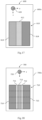
- FIG 9 is a schematic diagram of a diffractive optical waveguide 200 according to Embodiment 2 of the present disclosure.
- the diffractive optical waveguide 200 includes a waveguide substrate 200a, and a coupling-out grating 210 and a coupling-in grating 220 formed on the waveguide substrate 200a.
- the coupling-out grating 210 includes a first grating 211, a second grating 212, a third grating 213, a fourth grating 214, and a fifth grating 215 arranged side by side along the y direction, wherein the third grating 213 is arranged between the first grating 211 and the second grating 212, the fourth grating 214 and the fifth grating 215 are respectively arranged outside the first grating 211 and the second grating.
- the first grating 211, the second grating 212, and the third grating 213 respectively have the same grating structures as that of the first grating 111, the second grating 112, and the third grating 113 in the coupling-out grating 110 of the diffractive optical waveguide 100 shown in Figure 6 , it won't be repeated here.
- the fourth grating 214 is a one-dimensional grating and has a fourth grating vector G4
- the fifth grating 215 is a one-dimensional grating and has a fifth grating vector G5
- the fourth grating vector G4 and the fourth grating vector G5 are respectively the same as the second grating vector G2 and the third grating vector G3, the fourth grating vector G4 faces a direction away from the fifth grating, and the fifth grating vector G5 faces a direction away from the fourth grating.
- a wavelength of light is 532nm
- a refractive index of material of the waveguide substrate as well as the grating structure is 1.82
- a distance between the coupling-in grating and the coupling-out grating along the x direction is 20mm
- dimensions of the coupling-out grating in the x direction and y direction are 24mm and 28mm respectively.
- the optical unit structure is formed as a concave hole structure with a depth of 57nm, and in the array of the optical unit structure (including the first grating, the second grating, and the third grating) of the two-dimensional grating in the coupling-out grating as described above, the pitch D is equal to 420nm, the period P is equal to 485nm, and a staggered distance s is equal to P/2, so that the second grating vector G2 and the third grating vector G3 form an angle of 60° with respect to the x direction, and the first grating vector G1, the second grating vector G2 and the third grating vector G3 have the same magnitude.
- the diffractive optical waveguide 1 shown in Figure 1 the diffractive optical waveguide 2 shown in Figure 2 , the diffractive optical waveguide 100 shown in Figure 6 and the diffractive optical waveguide 200 shown in Figure 9 are simulated respectively, and parameters thereof are set as follows.
- the coupling-out grating 10 includes optical unit structures with rhombic cross-section profiles arranged in an array as described above, wherein a side length of the rhombic cross-section is 220 nm, and the upper and lower vertex angles are both 60°.
- the width w1 of the first grating 11 and the width w2 of the second grating 12 are both 9.5 mm, and the width w3 of the third grating 13 is 5 mm, and the optical unit structure of the third grating 13 has a rhombic cross-section profile, the side length of the rhombic cross-section is 220 nm, and the upper and lower vertex angles are 60°.
- the first grating 11 and the second grating 12 on both sides are one-dimensional wire gratings, respectively having the second grating vector G2 and the third grating vector G3, and a ridge width (the width of the convex structure) of the wire grating is 190.5 nm.
- the width w1 of the first grating 111 and the width w2 of the second grating 112 are both 9.5mm, and the width w3 of the third grating 113 is 5mm;
- the optical unit structure of the third grating 113 has a rhombic cross-section profile, the side length of the rhombic cross-section is 220nm, and the upper and lower vertex angles are 60°.
- the optical unit structure of the second grating 112 and the optical unit structure of the first grating 111 are symmetrical to each other with respect to the x axis.
- the width w1 of the first grating 211 and the width w2 the second grating 212 are both 2.5 mm
- the width w3 of the third grating 213 is 4mm
- the width w4 of the fourth grating 214 and the width w5 the fifth grating 215 are both 7.5mm.
- the optical unit structures of the first grating 211, the second grating 212, and the third grating 213 are respectively the same as that of the first grating 111, the second grating 112, and the third grating 113 in the diffractive optical waveguide 100 in Data Example 1.
- the fourth grating 214 and the fifth grating 215 are one-dimensional wire grating and respectively have the same structure parameters as that of the first grating 11 and the second grating 12 in the diffractive optical waveguide 2 in Data Example 1.
- field of view on both sides refers to the field of view with a field angle of view FOVX ranging from -10° to -6° and from 6° to 10° relative to the normal of the x-y plane in the direction around the x-axis
- the field of view in the middle refers to the field of view with the field angle of view FOVX ranging from -5° to 5°.
- the above-mentioned average efficiency is a ratio of an average value of the light intensity of the coupled-out light field at each field angle of view to the light intensity of the coupling-in light of the grating structure, and the larger the value of the average efficiency, the higher the coupling-out efficiency. Overhigh the coupled-out efficiency in the middle would result in a middle bright line shown in the display image of the waveguide.
- nonuniformity is a ratio of the maximum value of light intensity to the minimum value of light intensity in the entire field of view, and the smaller the value of nonuniformity, the better the uniformity.
- the diffractive optical waveguides 100 and 200 according to the embodiments of the present disclosure significantly reduce the nonuniformity of the output light field and achieve a great improvement in uniformity.
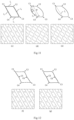
- the diffractive optical waveguide according to the embodiment of the present disclosure has been described above in conjunction with the optical unit structure having a parallelogram cross-section profile as shown in Figure 8 . It should be understood that the cross-section profile of the optical unit structure of the diffractive optical waveguide according to the embodiment of the present disclosure is not limited to a parallelogram. For ease of understanding, the following will be introduced in combination with different examples of the cross-section profiles of the optical unit structures shown in Figures 10 to 13 and in conjunction with Data Example 2.
- Figure 10 shows an example of a cross-section profile of the optical unit structure, which is a quadrilateral where the third straight line l3 and the fourth straight line l4 are not parallel to each other.
- Figure 11 shows an example where the profile lines between adjacent vertices are curves.
- Figure 12 and Figure 13 show different examples in which the profiles of the optical unit structures further include fifth vertices and sixth vertices, wherein Figure 12 shows an example in which the fifth vertex and the sixth vertex are, respectively, deviated inwardly with respect to the third straight line l 3 and the fourth straight line l 4 .
- Figure 13 shows an example where the fifth vertex and the sixth vertex are, respectively, deviated outward with respect to the third straight line l 3 and the fourth straight line l 4 , and an example where the fifth vertex and the sixth vertex are respectively, deviated in the same direction with respect to the third straight line l 3 and the fourth straight line l 4 .
- the first grating 211 in the diffractive optical waveguide 200 shown in Figure 9 is simulated and calculated by using the cross-section profiles of the optical unit structures shown in Figure 10 to Figure 13 and the examples (a) to (i) of the corresponding optical structures, and the parameters thereof are set as follows.
- the first straight line l 1 is parallel to the second straight line l 2
- the third straight line l 3 is parallel to the fourth straight line l 4
- the profile line C41 between the fourth vertex C4 and the first vertex C1 are curves, and expressions thereof are as follows.
- the first straight line l 1 is parallel to the second straight line l 2
- the third straight line l 3 is parallel to the fourth straight line l 4
- the profile line C12, the profile line C23, the profile line C34 and the profile line C41 are curves, and expressions are as follows.
- the first straight line l 1 is parallel to the second straight line l 2
- the third straight line l 3 is parallel to the fourth straight line l 4
- the profile line C12, the profile line C23, the profile line C34 and the profile line C41 are curves, and expressions are as follows
- the first straight line l 1 is parallel to the second straight line l 2
- the third straight line l 3 is parallel to the fourth straight line l 4
- the fifth vertex C5 is located between the first vertex C1 and the fourth vertex C4 along the circumferential direction and a distance from the fifth vertex C5 to the first vertex C1 is the same as that from the fifth vertex C5 to the fourth vertex C4
- the sixth vertex C6 is located between the second vertex C2 and the third vertex C3 along the circumferential direction and a distance from the sixth vertex C6 to the second vertex C2 is the same as that from the sixth vertex C6 to the third vertex C3
- examples of (x, y) coordinates of the first vertex C1, the second vertex C2, the third vertex C3, the fourth vertex C4, the fifth vertex C5 and the sixth vertex C6 are shown in Table 2.
- Vertex C1 C2 C3 C4 C5 C6 Coordinate (nm) (-176,-249) (-176,47) (176,249) (176,-47) (0,-132) (0,132) wherein, the profile lines between adjacent vertices are straight lines.
- the first straight line l 1 is parallel to the second straight line l 2
- the third straight line l 3 is parallel to the fourth straight line l 4
- the fifth vertex C5 is located between the first vertex C1 and the fourth vertex C4 along the circumferential direction and a distance from the fifth vertex C5 to the first vertex C1 is the same as that from the fifth vertex C5 to the fourth vertex C4
- the sixth vertex C6 is located between the second vertex C2 and the third vertex C3 along the circumferential direction and a distance from the sixth vertex C6 to the second vertex C2 is the same as that from the sixth vertex C6 to the third vertex C3
- examples of (x, y) coordinates of the first vertex C1, the second vertex C2, the third vertex C3, the fourth vertex C4, the fifth vertex C5 and the sixth vertex C6 are shown in Table 3. [Table 3] Vertex C
- the profile line C12, the profile line C26, the profile line C63, the profile line C34, the profile line C45, and the profile line C51 between adjacent vertices are curves, and the expressions are as follows.
- the first straight line l 1 is parallel to the second straight line l 2
- the third straight line l 3 is parallel to the fourth straight line l 4
- the fifth vertex C5 is located between the first vertex C1 and the fourth vertex C4 along the circumferential direction and a distance from the fifth vertex C5 to the first vertex C1 is the same as that from the fifth vertex C5 to the fourth vertex C4
- the sixth vertex C6 is located between the second vertex C2 and the third vertex C3 along the circumferential direction and a distance from the sixth vertex C6 to the second vertex C2 is the same as that from the sixth vertex C6 to the third vertex C3
- examples of (x, y) coordinates of the first vertex C1, the second vertex C2, the third vertex C3, the fourth vertex C4, the fifth vertex C5 and the sixth vertex C6 are shown in Table 4. [Table 4] Vertex C1
- the profile line C12, the profile line C26, the profile line C63, the profile line C34, the profile line C45, and the profile line C51 between adjacent vertices are curves, and the expressions are as follows.
- the straight line extending through the first vertex and the fifth vertex and the straight line extending through the third vertex and the sixth vertex are parallel to each other, and the straight line extending through the fourth vertex and the fifth vertex and the straight line extending through the second vertex and the sixth vertex are parallel to each other.
- the straight line extending through the first vertex and the fifth vertex and the straight line extending through the second vertex and the sixth vertex are parallel to each other, and the straight line extending through the fourth vertex and the fifth vertex and the straight line extending through the third vertex and the sixth vertex are parallel to each other.
- the coupled-out efficiency and nonuniformity indices of different diffractive optical waveguides at the central position of the eyebox are calculated by simulation, as shown in Table 5.
- the third straight line and the fourth straight line are not limited to the case of being parallel to each other, when the two are not parallel, it is still beneficial to improve the uniformity of the output light field of the diffractive optical waveguide.
- the profile lines between adjacent vertices can be curves, and when the ratio of the deviation of the profile line between two vertices from the straight line extending through the two vertices to the distance between the two vertices is less than or equal to one-fifth, better coupled-out efficiency of diffractive optical waveguide and uniformity of the output light field (see Example (c) and Example (e)) can be obtained, while as the above ratio increases, the nonuniformity increases and the uniformity deteriorates (see Example (d)).
- Example (f) Compared Example (f) and Example (g), it can be seen that the cross-section of the optical unit structure in Example (g) has a much smooth profile due to chamfering, which is convenient for processing and restoration of the design, and at the same time, it can be seen from the simulation results that Example (g) can achieve similar or even better results than Example (f), especially in terms of uniformity.
- the first grating in the diffractive optical waveguide according to the embodiment of the present disclosure can have a curve profile structure, its smooth edge has very good processability and can achieve high-precision restoration and mass production.
- the curve profile structure has a very high degree of design freedom, which is beneficial to better control of efficiency distribution.
- profile lines between adjacent vertices in the same profile are all straight lines or curves, however, according to other embodiments of the present disclosure, these profile lines may include a straight line and a curve at the same time.
- diffractive optical waveguides according to other embodiments of the present disclosure will be introduced with reference to Figures 14 to 18 , wherein gratings (such as the first grating, the second grating, etc.) with different grating structures of the coupling-out gratings in the diffractive optical waveguides have more diverse setting modes.
- gratings such as the first grating, the second grating, etc.
- FIG 14 is a schematic diagram of a diffractive optical waveguide 300 according to Embodiment 3 of the present disclosure.
- the diffractive optical waveguide 300 shown in Figure 14 has basically the same structure as that of the diffractive optical waveguide 100 shown in Figure 6 , and the differences lie in that, a coupling-in grating 320 can be offset with respect to a coupling-out grating 310 in the diffractive optical waveguide 300, and the direction of the first grating vector G 1 (that is, the x direction) of a first grating 311, a second grating 312 and a third grating 313 in the coupling-out grating 310 is parallel to the direction of light propagation (that is, the coupling-in direction) from the coupling-in grating 320 to the coupling-out grating 310 within the waveguide substrate 300a.
- the first grating 311, the second grating 312, and the third grating 313 can still be considered to be arranged side by side along the y direction perpendicular to the x direction, but they can be arranged obliquely with respect to the edge of the overall shape of the coupling-out grating 310.
- FIG 15 is a schematic diagram of a diffractive optical waveguide 400 according to Embodiment 4 of the present disclosure.
- the diffractive optical waveguide 400 shown in Figure 15 has basically the same structure as that of the diffractive optical waveguide 200 shown in Figure 9 , and the differences lie in that, a coupling-in grating 420 can be offset with respect to a coupling-out grating 410 in the diffractive optical waveguide 400, and the direction of the first grating vector G 1 (that is, the x direction) of a first grating 411, a second grating 412 and a third grating 413 in the coupling-out grating 410 is parallel to the direction of light propagation (that is, the coupling-in direction) from the coupling-in grating 420 to the coupling-out grating 410 within the waveguide substrate 400a.
- the first grating 411, the second grating 412, and the third grating 413 can still be considered to be arranged side by side along the y direction perpendicular to the x direction, but they can be arranged obliquely with respect to the edge of the overall shape of the coupling-out grating 410.
- the light carrying image information coupled into the diffractive optical waveguide has a certain range of field of view angle
- “coupling-in direction” refers to the direction in which the central light beam within the range of the field of view angle propagates to the coupling-out grating within the waveguide substrate.
- the direction of the first grating vector G 1 that is, the x direction
- the coupling-out grating in the diffractive optical waveguide may not be completely consistent with the coupling-in direction, for example, there may be an angle deviation of 0-5° between the two directions.
- FIG 16 is a schematic diagram of a diffractive optical waveguide 500 according to Embodiment 5 of the present disclosure.
- a coupling-in grating 520 can be offset with respect to a coupling-out grating 510 in the diffractive optical waveguide 500, and the coupling-out grating 510 only includes a first grating 511 and a third grating 513, without including the second grating introduced in the above embodiments.
- the third grating 513 in the coupling-out grating 510 can be arranged opposite to the coupling-in grating 520.
- FIG 17 is a schematic diagram of a diffractive optical waveguide 600 according to Embodiment 6 of the present disclosure.
- a coupling-in grating 620 can be offset with respect to a coupling-out grating 610 in the diffractive optical waveguide 600, and the coupling-out grating 610 only includes a first grating 611, a third grating 613, and a fourth grating 614 located on the opposite side of the third grating 613 relative to the first grating 611, without including a second grating and a fifth grating.
- the fourth grating is a one-dimensional grating and its grating vector is oriented away from the first grating 611. In this way, the third grating 613 in the coupling-out grating 610 can be arranged opposite to the coupling-in grating 620.
- FIG. 14 to 17 provide more layout schemes of diffractive optical waveguides for the case where the coupling-in grating is offset with respect to the coupling-out grating.
- FIG 18 is a schematic diagram of a diffractive optical waveguide 700 according to Embodiment 7 of the present disclosure.
- the diffractive optical waveguide 700 may have substantially the same structure as that of the diffractive optical waveguide 200 shown in Figure 9 , and the differences lie in that, each sub-grating of coupling-out grating 710 (including a first grating 711, a second grating 712, a third grating 713, a fourth grating 714, and a fifth grating 715) is divided into more than two subareas, and each sub-grating may have different optical unit structures in its subareas.
- the first grating 711 may have optical unit structures with different cross-section profiles as shown in Figures 10-13 in its subareas, thus providing a very flexible means for regulating the coupled-out efficiency of diffractive optical waveguide 700 in different regions and different field of view regions and regulating the uniformity of the output light field. This is beneficial to the design and manufacture of diffractive optical waveguides.
- the diffractive optical waveguide according to the embodiment of the present disclosure can be applied in a display apparatus.
- a display apparatus is, for example, a near-eye display apparatus, which includes a lens and a frame for holding the lens close to the eye, the lens including a diffractive optical waveguide according to an embodiment of the present disclosure as described above.
- the display apparatus may be an augmented reality display apparatus or a virtual reality display apparatus.
Landscapes
- Physics & Mathematics (AREA)
- General Physics & Mathematics (AREA)
- Optics & Photonics (AREA)
- Optical Couplings Of Light Guides (AREA)
Applications Claiming Priority (1)
| Application Number | Priority Date | Filing Date | Title |
|---|---|---|---|
| CN202210924670.7A CN115016057B (zh) | 2022-08-03 | 2022-08-03 | 衍射光波导以及具有其的显示设备 |
Publications (3)
| Publication Number | Publication Date |
|---|---|
| EP4343393A1 true EP4343393A1 (fr) | 2024-03-27 |
| EP4343393B1 EP4343393B1 (fr) | 2025-02-26 |
| EP4343393C0 EP4343393C0 (fr) | 2025-02-26 |
Family
ID=83065851
Family Applications (1)
| Application Number | Title | Priority Date | Filing Date |
|---|---|---|---|
| EP23188917.1A Active EP4343393B1 (fr) | 2022-08-03 | 2023-08-01 | Guide d'ondes optique diffractif et appareil d'affichage le comprenant |
Country Status (3)
| Country | Link |
|---|---|
| US (1) | US11874488B1 (fr) |
| EP (1) | EP4343393B1 (fr) |
| CN (1) | CN115016057B (fr) |
Families Citing this family (12)
| Publication number | Priority date | Publication date | Assignee | Title |
|---|---|---|---|---|
| WO2022086002A1 (fr) * | 2020-10-20 | 2022-04-28 | Samsung Electronics Co., Ltd. | Structure de guide d'ondes à éléments optiques diffractifs segmentés et appareil d'affichage proche de l'œil l'utilisant |
| CN115482769A (zh) * | 2021-05-31 | 2022-12-16 | 京东方科技集团股份有限公司 | 像素驱动电路及其驱动方法、显示基板 |
| CN115185029B (zh) * | 2022-09-07 | 2023-02-17 | 北京驭光科技发展有限公司 | 光栅结构、衍射光波导以及显示设备 |
| CN117761823A (zh) * | 2022-09-19 | 2024-03-26 | 歌尔光学科技有限公司 | 光波导器件及头戴显示设备 |
| WO2024093642A1 (fr) * | 2022-10-31 | 2024-05-10 | 上海鲲游科技有限公司 | Structure de réseau de couplage d'entrée, guide d'ondes optique de diffraction et dispositif de réalité augmentée |
| CN115793119B (zh) * | 2023-01-09 | 2023-04-18 | 北京驭光科技发展有限公司 | 衍射光波导及显示设备 |
| CN115793132B (zh) * | 2023-01-29 | 2023-07-25 | 北京亮亮视野科技有限公司 | 二维衍射光栅波导结构和近眼显示设备 |
| CN116299814A (zh) * | 2023-03-07 | 2023-06-23 | 珠海莫界科技有限公司 | 衍射光栅、光波导装置以及显示设备 |
| CN116466422A (zh) * | 2023-03-07 | 2023-07-21 | 珠海莫界科技有限公司 | 衍射光栅、光波导装置以及显示设备 |
| US12477096B2 (en) * | 2023-08-04 | 2025-11-18 | Htc Corporation | Calibration method, electronic device, and non-transitory computer readable storage medium |
| CN117608021A (zh) * | 2023-10-30 | 2024-02-27 | 驭光科技(北京)有限公司 | 防漏光衍射光波导装置及具有其的显示设备 |
| CN119493208A (zh) * | 2024-11-27 | 2025-02-21 | 深圳市光舟半导体技术有限公司 | 光波导及显示设备 |
Citations (5)
| Publication number | Priority date | Publication date | Assignee | Title |
|---|---|---|---|---|
| WO2022011026A1 (fr) * | 2020-07-09 | 2022-01-13 | Vuzix Corporation | Guide de lumière d'image avec élément optique diffractif composé et dispositif d'affichage monté sur la tête fabriqué avec celui-ci |
| CN215641931U (zh) * | 2021-07-30 | 2022-01-25 | Oppo广东移动通信有限公司 | 光学结构和光学装置 |
| WO2022060743A1 (fr) * | 2020-09-16 | 2022-03-24 | Magic Leap, Inc. | Oculaires destinés à un système d'affichage à réalité augmentée |
| WO2022115580A1 (fr) * | 2020-11-25 | 2022-06-02 | Vuzix Corporation | Guide de lumière d'image avec optique diffractive zonée |
| US20220206300A1 (en) * | 2019-03-13 | 2022-06-30 | Lg Chem, Ltd. | Diffraction light guide plate |
Family Cites Families (7)
| Publication number | Priority date | Publication date | Assignee | Title |
|---|---|---|---|---|
| US7364341B2 (en) * | 1999-02-23 | 2008-04-29 | Solid State Opto Limited | Light redirecting films including non-interlockable optical elements |
| US9187175B1 (en) * | 2013-10-31 | 2015-11-17 | Franklin Y. K. Chen | Flying-wing and VTOL flying-wing aircraft |
| CN113281839B (zh) * | 2017-06-13 | 2023-04-14 | 伊奎蒂公司 | 具有扩大光分布重叠光栅的图像光导 |
| CN113325507A (zh) * | 2018-12-26 | 2021-08-31 | 上海鲲游光电科技有限公司 | 一种基于二维光栅的平面光波导 |
| US10935730B1 (en) * | 2019-11-25 | 2021-03-02 | Shanghai North Ocean Photonics Co., Ltd. | Waveguide display device |
| CN113325579A (zh) * | 2020-02-28 | 2021-08-31 | 苏州苏大维格科技集团股份有限公司 | 用于呈现增强现实图像的装置和包含该装置的系统 |
| JP7198245B2 (ja) | 2020-09-02 | 2022-12-28 | Kddi株式会社 | 周波数帯域の優先度に従ってセル選択を実行する端末装置、その制御方法、およびプログラム |
-
2022
- 2022-08-03 CN CN202210924670.7A patent/CN115016057B/zh active Active
-
2023
- 2023-07-11 US US18/350,658 patent/US11874488B1/en active Active
- 2023-08-01 EP EP23188917.1A patent/EP4343393B1/fr active Active
Patent Citations (5)
| Publication number | Priority date | Publication date | Assignee | Title |
|---|---|---|---|---|
| US20220206300A1 (en) * | 2019-03-13 | 2022-06-30 | Lg Chem, Ltd. | Diffraction light guide plate |
| WO2022011026A1 (fr) * | 2020-07-09 | 2022-01-13 | Vuzix Corporation | Guide de lumière d'image avec élément optique diffractif composé et dispositif d'affichage monté sur la tête fabriqué avec celui-ci |
| WO2022060743A1 (fr) * | 2020-09-16 | 2022-03-24 | Magic Leap, Inc. | Oculaires destinés à un système d'affichage à réalité augmentée |
| WO2022115580A1 (fr) * | 2020-11-25 | 2022-06-02 | Vuzix Corporation | Guide de lumière d'image avec optique diffractive zonée |
| CN215641931U (zh) * | 2021-07-30 | 2022-01-25 | Oppo广东移动通信有限公司 | 光学结构和光学装置 |
Also Published As
| Publication number | Publication date |
|---|---|
| US11874488B1 (en) | 2024-01-16 |
| EP4343393B1 (fr) | 2025-02-26 |
| CN115016057A (zh) | 2022-09-06 |
| US20240045132A1 (en) | 2024-02-08 |
| EP4343393C0 (fr) | 2025-02-26 |
| CN115016057B (zh) | 2022-11-04 |
Similar Documents
| Publication | Publication Date | Title |
|---|---|---|
| EP4343393A1 (fr) | Guide d'ondes optique diffractif et appareil d'affichage le comprenant | |
| US20240272427A1 (en) | Optical waveguide device for diffraction display and display device | |
| KR102751421B1 (ko) | 광 가이드 광학 어셈블리 | |
| CN113777707A (zh) | 光学结构和光学装置 | |
| CN113495319A (zh) | 光学结构和光学装置 | |
| EP4293280A1 (fr) | Guide d'ondes optique diffractif, procédé de conception et procédé de formation de celui-ci, et dispositif d'affichage | |
| EP4293410A1 (fr) | Guide d'ondes optique diffractif et dispositif d'affichage le comprenant | |
| US11892682B2 (en) | Diffractive optical waveguide and display device having the same preliminary class | |
| CN112965167A (zh) | 一种高效率光栅波导光学元件 | |
| US11846785B1 (en) | Diffraction optical waveguide and grating structure thereof, and display device | |
| CN215641931U (zh) | 光学结构和光学装置 | |
| CN117608021A (zh) | 防漏光衍射光波导装置及具有其的显示设备 | |
| CN218240461U (zh) | 一种波导片及近眼显示设备 | |
| US20250199321A1 (en) | Diffractive optical waveguide, design method and formation method thereof, and display device | |
| US20190148911A1 (en) | Techniques for providing curved facet semiconductor lasers | |
| CN114784616A (zh) | 一种集成超透镜的锥形半导体激光器 | |
| CN118377081B (zh) | 导光器件、光学显示系统及显示设备 | |
| US12085762B2 (en) | Optical waveguide device for image display and display device having the same | |
| CN112859231A (zh) | 一种光栅波导光学器件 | |
| CN219609346U (zh) | 光波导系统以及近眼显示设备 | |
| CN118707652A (zh) | 光波导结构和ar显示设备 | |
| US20240118557A1 (en) | Optical structure and optical device | |
| CN223155315U (zh) | 衍射光波导装置 | |
| CN121634513A (zh) | 一种衍射光波导的设计方法及衍射光波导 | |
| CN118057217A (zh) | 一种衍射光波导 |
Legal Events
| Date | Code | Title | Description |
|---|---|---|---|
| PUAI | Public reference made under article 153(3) epc to a published international application that has entered the european phase |
Free format text: ORIGINAL CODE: 0009012 |
|
| STAA | Information on the status of an ep patent application or granted ep patent |
Free format text: STATUS: REQUEST FOR EXAMINATION WAS MADE |
|
| 17P | Request for examination filed |
Effective date: 20230801 |
|
| AK | Designated contracting states |
Kind code of ref document: A1 Designated state(s): AL AT BE BG CH CY CZ DE DK EE ES FI FR GB GR HR HU IE IS IT LI LT LU LV MC ME MK MT NL NO PL PT RO RS SE SI SK SM TR |
|
| GRAP | Despatch of communication of intention to grant a patent |
Free format text: ORIGINAL CODE: EPIDOSNIGR1 |
|
| STAA | Information on the status of an ep patent application or granted ep patent |
Free format text: STATUS: GRANT OF PATENT IS INTENDED |
|
| INTG | Intention to grant announced |
Effective date: 20241212 |
|
| GRAS | Grant fee paid |
Free format text: ORIGINAL CODE: EPIDOSNIGR3 |
|
| GRAA | (expected) grant |
Free format text: ORIGINAL CODE: 0009210 |
|
| STAA | Information on the status of an ep patent application or granted ep patent |
Free format text: STATUS: THE PATENT HAS BEEN GRANTED |
|
| AK | Designated contracting states |
Kind code of ref document: B1 Designated state(s): AL AT BE BG CH CY CZ DE DK EE ES FI FR GB GR HR HU IE IS IT LI LT LU LV MC ME MK MT NL NO PL PT RO RS SE SI SK SM TR |
|
| REG | Reference to a national code |
Ref country code: GB Ref legal event code: FG4D |
|
| REG | Reference to a national code |
Ref country code: CH Ref legal event code: EP |
|
| REG | Reference to a national code |
Ref country code: DE Ref legal event code: R096 Ref document number: 602023002192 Country of ref document: DE |
|
| REG | Reference to a national code |
Ref country code: IE Ref legal event code: FG4D |
|
| U01 | Request for unitary effect filed |
Effective date: 20250226 |
|
| U07 | Unitary effect registered |
Designated state(s): AT BE BG DE DK EE FI FR IT LT LU LV MT NL PT RO SE SI Effective date: 20250304 |
|
| PG25 | Lapsed in a contracting state [announced via postgrant information from national office to epo] |
Ref country code: RS Free format text: LAPSE BECAUSE OF FAILURE TO SUBMIT A TRANSLATION OF THE DESCRIPTION OR TO PAY THE FEE WITHIN THE PRESCRIBED TIME-LIMIT Effective date: 20250526 |
|
| PG25 | Lapsed in a contracting state [announced via postgrant information from national office to epo] |
Ref country code: PL Free format text: LAPSE BECAUSE OF FAILURE TO SUBMIT A TRANSLATION OF THE DESCRIPTION OR TO PAY THE FEE WITHIN THE PRESCRIBED TIME-LIMIT Effective date: 20250226 |
|
| PG25 | Lapsed in a contracting state [announced via postgrant information from national office to epo] |
Ref country code: ES Free format text: LAPSE BECAUSE OF FAILURE TO SUBMIT A TRANSLATION OF THE DESCRIPTION OR TO PAY THE FEE WITHIN THE PRESCRIBED TIME-LIMIT Effective date: 20250226 |
|
| PG25 | Lapsed in a contracting state [announced via postgrant information from national office to epo] |
Ref country code: NO Free format text: LAPSE BECAUSE OF FAILURE TO SUBMIT A TRANSLATION OF THE DESCRIPTION OR TO PAY THE FEE WITHIN THE PRESCRIBED TIME-LIMIT Effective date: 20250526 Ref country code: IS Free format text: LAPSE BECAUSE OF FAILURE TO SUBMIT A TRANSLATION OF THE DESCRIPTION OR TO PAY THE FEE WITHIN THE PRESCRIBED TIME-LIMIT Effective date: 20250626 |
|
| PG25 | Lapsed in a contracting state [announced via postgrant information from national office to epo] |
Ref country code: HR Free format text: LAPSE BECAUSE OF FAILURE TO SUBMIT A TRANSLATION OF THE DESCRIPTION OR TO PAY THE FEE WITHIN THE PRESCRIBED TIME-LIMIT Effective date: 20250226 |
|
| PG25 | Lapsed in a contracting state [announced via postgrant information from national office to epo] |
Ref country code: GR Free format text: LAPSE BECAUSE OF FAILURE TO SUBMIT A TRANSLATION OF THE DESCRIPTION OR TO PAY THE FEE WITHIN THE PRESCRIBED TIME-LIMIT Effective date: 20250527 |
|
| U20 | Renewal fee for the european patent with unitary effect paid |
Year of fee payment: 3 Effective date: 20250826 |
|
| PG25 | Lapsed in a contracting state [announced via postgrant information from national office to epo] |
Ref country code: SM Free format text: LAPSE BECAUSE OF FAILURE TO SUBMIT A TRANSLATION OF THE DESCRIPTION OR TO PAY THE FEE WITHIN THE PRESCRIBED TIME-LIMIT Effective date: 20250226 |
|
| PG25 | Lapsed in a contracting state [announced via postgrant information from national office to epo] |
Ref country code: CZ Free format text: LAPSE BECAUSE OF FAILURE TO SUBMIT A TRANSLATION OF THE DESCRIPTION OR TO PAY THE FEE WITHIN THE PRESCRIBED TIME-LIMIT Effective date: 20250226 |
|
| PG25 | Lapsed in a contracting state [announced via postgrant information from national office to epo] |
Ref country code: SK Free format text: LAPSE BECAUSE OF FAILURE TO SUBMIT A TRANSLATION OF THE DESCRIPTION OR TO PAY THE FEE WITHIN THE PRESCRIBED TIME-LIMIT Effective date: 20250226 |
|
| PLBE | No opposition filed within time limit |
Free format text: ORIGINAL CODE: 0009261 |
|
| STAA | Information on the status of an ep patent application or granted ep patent |
Free format text: STATUS: NO OPPOSITION FILED WITHIN TIME LIMIT |
|
| 26N | No opposition filed |
Effective date: 20251127 |
|
| PG25 | Lapsed in a contracting state [announced via postgrant information from national office to epo] |
Ref country code: MC Free format text: LAPSE BECAUSE OF FAILURE TO SUBMIT A TRANSLATION OF THE DESCRIPTION OR TO PAY THE FEE WITHIN THE PRESCRIBED TIME-LIMIT Effective date: 20250226 |