EP4346073A1 - Leistungswandler mit dynamischer strommessungszeit - Google Patents
Leistungswandler mit dynamischer strommessungszeit Download PDFInfo
- Publication number
- EP4346073A1 EP4346073A1 EP22197892.7A EP22197892A EP4346073A1 EP 4346073 A1 EP4346073 A1 EP 4346073A1 EP 22197892 A EP22197892 A EP 22197892A EP 4346073 A1 EP4346073 A1 EP 4346073A1
- Authority
- EP
- European Patent Office
- Prior art keywords
- power converter
- current
- current sensing
- switching frequency
- timing circuit
- Prior art date
- Legal status (The legal status is an assumption and is not a legal conclusion. Google has not performed a legal analysis and makes no representation as to the accuracy of the status listed.)
- Pending
Links
Images


Classifications
-
- H—ELECTRICITY
- H02—GENERATION; CONVERSION OR DISTRIBUTION OF ELECTRIC POWER
- H02M—APPARATUS FOR CONVERSION BETWEEN AC AND AC, BETWEEN AC AND DC, OR BETWEEN DC AND DC, AND FOR USE WITH MAINS OR SIMILAR POWER SUPPLY SYSTEMS; CONVERSION OF DC OR AC INPUT POWER INTO SURGE OUTPUT POWER; CONTROL OR REGULATION THEREOF
- H02M1/00—Details of apparatus for conversion
- H02M1/0003—Details of control, feedback or regulation circuits
- H02M1/0009—Devices or circuits for detecting current in a converter
-
- G—PHYSICS
- G01—MEASURING; TESTING
- G01R—MEASURING ELECTRIC VARIABLES; MEASURING MAGNETIC VARIABLES
- G01R19/00—Arrangements for measuring currents or voltages or for indicating presence or sign thereof
- G01R19/25—Arrangements for measuring currents or voltages or for indicating presence or sign thereof using digital measurement techniques
- G01R19/2506—Arrangements for conditioning or analysing measured signals, e.g. for indicating peak values ; Details concerning sampling, digitizing or waveform capturing
- G01R19/2509—Details concerning sampling, digitizing or waveform capturing
-
- H—ELECTRICITY
- H02—GENERATION; CONVERSION OR DISTRIBUTION OF ELECTRIC POWER
- H02M—APPARATUS FOR CONVERSION BETWEEN AC AND AC, BETWEEN AC AND DC, OR BETWEEN DC AND DC, AND FOR USE WITH MAINS OR SIMILAR POWER SUPPLY SYSTEMS; CONVERSION OF DC OR AC INPUT POWER INTO SURGE OUTPUT POWER; CONTROL OR REGULATION THEREOF
- H02M3/00—Conversion of DC power input into DC power output
- H02M3/22—Conversion of DC power input into DC power output with intermediate conversion into AC
- H02M3/24—Conversion of DC power input into DC power output with intermediate conversion into AC by static converters
- H02M3/28—Conversion of DC power input into DC power output with intermediate conversion into AC by static converters using discharge tubes with control electrode or semiconductor devices with control electrode to produce the intermediate AC
- H02M3/325—Conversion of DC power input into DC power output with intermediate conversion into AC by static converters using discharge tubes with control electrode or semiconductor devices with control electrode to produce the intermediate AC using devices of a triode or a transistor type requiring continuous application of a control signal
- H02M3/335—Conversion of DC power input into DC power output with intermediate conversion into AC by static converters using discharge tubes with control electrode or semiconductor devices with control electrode to produce the intermediate AC using devices of a triode or a transistor type requiring continuous application of a control signal using semiconductor devices only
- H02M3/33569—Conversion of DC power input into DC power output with intermediate conversion into AC by static converters using discharge tubes with control electrode or semiconductor devices with control electrode to produce the intermediate AC using devices of a triode or a transistor type requiring continuous application of a control signal using semiconductor devices only having several active switching elements
- H02M3/33576—Conversion of DC power input into DC power output with intermediate conversion into AC by static converters using discharge tubes with control electrode or semiconductor devices with control electrode to produce the intermediate AC using devices of a triode or a transistor type requiring continuous application of a control signal using semiconductor devices only having several active switching elements having at least one active switching element at the secondary side of an isolation transformer
- H02M3/33592—Conversion of DC power input into DC power output with intermediate conversion into AC by static converters using discharge tubes with control electrode or semiconductor devices with control electrode to produce the intermediate AC using devices of a triode or a transistor type requiring continuous application of a control signal using semiconductor devices only having several active switching elements having at least one active switching element at the secondary side of an isolation transformer having a synchronous rectifier circuit or a synchronous freewheeling circuit at the secondary side of an isolation transformer
-
- H—ELECTRICITY
- H05—ELECTRIC TECHNIQUES NOT OTHERWISE PROVIDED FOR
- H05B—ELECTRIC HEATING; ELECTRIC LIGHT SOURCES NOT OTHERWISE PROVIDED FOR; CIRCUIT ARRANGEMENTS FOR ELECTRIC LIGHT SOURCES, IN GENERAL
- H05B45/00—Circuit arrangements for operating light-emitting diodes [LED]
- H05B45/30—Driver circuits
- H05B45/37—Converter circuits
- H05B45/3725—Switched mode power supply [SMPS]
- H05B45/385—Switched mode power supply [SMPS] using flyback topology
Definitions
- the invention relates to a power converter, preferably a synchronous flyback converter. Especially, the invention relates to measuring a current within the converter.
- the document EP 4 054 066 A1 shows a synchronous flyback converter.
- the object of the invention is to provide a power converter, which achieves a simple and reliable current measurement.
- a power converter comprises a current sensing circuit, which is configured to sample a sensing current during a current sampling time window.
- the current sampling time window begins at a current sampling start time.
- the power converter comprises a current sensing timing circuit, which is configured to adjust the current sampling start time.
- the current sensing timing circuit is configured to adjust the current sampling start time based on a switching frequency of the power converter. This allows for counteracting effects of the switching frequency on the optimum current sampling time.
- the sensing timing circuit is moreover configured to adjust the current sampling start time to a first time for a first switching frequency of the power converter, and to a second time for a second switching frequency of the power converter.
- the first time therein is later than the second time, and the first switching frequency of the power converter is lower than the second switching frequency of the power converter. This allows for compensating that the optimum sampling time is sooner for higher switching frequencies and later for lower switching frequencies.
- the power converter comprises a primary side switch configured to repeatedly switch on and off during the operation of the power converter.
- the sensing timing circuit is configured to adjust the current sampling start time to be a correction time interval after a switching on of the primary side switch. This allows for a simple and reliable start of the sampling.
- the power converter comprises a primary side switch and a secondary side switch.
- the primary side switch and the secondary side switch are configured to alternatingly switch on and off during operation of the power converter. It should be mentioned here that the switches are preferably not switched on simultaneously. It should also be mentioned here that between the switching on and off of the switches, a dead time in which none of the switches is switched on, exists.
- the sensing timing circuit is configured to adjust the current sampling start time to be a correction time interval plus a dead time interval after a switching off of the secondary side switch. This allows for a longer time interval from the triggering condition to start the sampling to the actual begin of the sampling. This allows for a simpler circuit construction.
- the dead time interval is a constant time interval.
- the sensing timing circuit is moreover configured to adjust the current sampling start time by adjusting a length of the correction time interval. This allows for a highly accurate timing adjustment.
- the sensing timing circuit is configured to adjust the correction time interval based on the switching frequency of the power converter. This allows for a very simple adjustment of the sampling time while achieving high sampling accuracy.
- the sensing timing circuit is configured to adjust the correction time interval to a first value for a first switching frequency of the power converter, and to a second value for a second switching frequency of the power converter.
- the first value is higher than the second value.
- the first switching frequency of the power converter is lower than the second switching frequency of the power converter. This allows for an especially high accuracy of the sampling.
- the sensing timing circuit is configured to adjust the correction time interval by multiplying a default correction time interval with a correction value, dependent on the switching frequency of the power converter.
- the sensing timing circuit is configured to adjust the correction time interval by adding a correction value, dependent on the switching frequency of the power converter to a default correction time interval.
- the first option allows for an especially high accuracy of the adjustment, while the second option allows for an especially low computational power to perform the adjustment.
- the correction value comprises an inverse of the switching frequency. This allows for an especially simple determining of the correction value.
- the current sensing timing circuit comprises a correction value determiner, configured to iteratively determine a suitable correction value by increasing the correction value when the current sensing circuit detects a drop off of the sensing current by more than a first threshold during a first part of the current sampling time window, and by decreasing the correction value when the current sensing circuit detects an increase of the sensing current by more than a second threshold during a last part of the current sampling time window. Dynamic factors, such as temperature or humidity can thereby be compensated.
- the power converter is a flyback power converter, preferably a synchronized flyback power converter.
- the power converter then comprises a primary side and a secondary side.
- the secondary side then comprises a damping resistor connected in parallel to an inductor on the secondary side.
- the inductor and the parallel-connected damping resistor are connected in series to a capacitor, preferably an electrolytic capacitor.
- the current sensing circuit is configured to measure the sensing current by measuring a sensing voltage at the current sensing resistor located on the primary side. This allows for an especially simple circuit construction.
- the current sensing circuit is implemented by a first microcontroller.
- the current sensing timing circuit is implemented by a second microcontroller.
- the first microcontroller and the second microcontroller are different microcontrollers.
- the first microcontroller and the second microcontroller are the same microcontroller.
- the power converter is configured to power at least one LED. This allows for a broad application scope of the power converter.
- a lighting assembly comprises a power converter according to the first aspect of the invention, and at least one LED. This allows for an especially efficient operation of the LED, and an especially simple circuit construction.
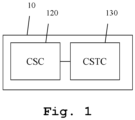
- the power converter 10 comprises a current sensing circuit 120 and a current sensing timing circuit 130.
- the current sensing circuit is configured to sample a sensing current during a current sampling time window.
- the current sampling time window begins at a current sampling start time.
- the current sensing timing circuit 130 is configured to adjust the current sampling start time. Thereby, an optimum current sampling can be achieved, since the current sampling time window can thereby be placed at an optimum position.
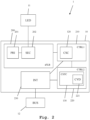
- the power converter 10 comprises a synchronized flyback 200, a first controller 210, a second controller 220, and an interface 230.
- the synchronized flyback 200 is connected to the first controller 210, which in turn is connected to the second controller 220, which again is connected to the interface 230.
- the synchronized flyback 200 comprises a primary side 201 and a secondary side 202 (defined with reference to the isolation by the flyback transformer).
- the secondary side 202 may be connected to at least one LED 11, which is not part of the power converter 10.
- the first controller 210 comprises the current sensing circuit 120, already described along Fig. 1 .
- the second controller 220 comprises the current sensing timing circuit 130, already explained along Fig. 1 .
- the current sensing timing circuit 130 may further comprise a correction value determiner 221.
- the first controller 210 and the second controller 220 although depicted as separate controllers here, can be implemented as a single controller. Especially, the controllers can be implemented as ASICs or DSPs.
- the interface 230 may moreover be connected with external devices, such as a bus 12, as depicted here. Also, a direct connection to a switch or a different signal source is possible through the interface 230.
- the first controller 210 controls the operation of the primary side switch on the primary side 201 and the secondary switch of the secondary side 202.
- the switches are operated alternatingly with a dead time between the on-times of the switches.
- the current sensing circuit 120 determines the operating current on the secondary side.
- the operating current is measured during a current sampling time window.
- the current sampling timing circuit 130 adjusts the start time of the current sampling time window.
- the correction value determiner 221 may perform a dynamic adjustment of a correction value for correcting the start time of the current sampling time window, if it is present.
- Fig. 3 a circuit diagram of the power converter 10 is shown.
- the power converter 10 here comprises the previously described primary side 201 and secondary side 202.
- the here-depicted power converter 10 moreover comprises an electromagnetic interference stage 300 and a power factor correction stage 310. These stages, though, are not relevant to the present invention and are only depicted here for reasons of completeness.
- the primary side 201 comprises an inductance L40.
- the winding L40b is part of the primary side, while the inductance L40 constitutes the connection to the secondary side 202.
- the primary side 201 moreover comprises a primary side switch M1, which is implemented as a transistor.
- the control terminal of the primary side switch M1 is connected to a drive signal input DRV1.
- the winding L40b is connected on its one side to the primary side switch M1, and on its other side to a bus voltage VBUS.
- the primary side switch M1 is furthermore connected to a resistor R52, which is connected to ground at its other terminal. The connection between the primary side switch M1 and the resistor R52 is used as a first voltage sensing location.
- the secondary side 202 is also connected to the inductance L40.
- the windings L40c and L40d are considered part of the secondary side 202.
- the windings L40c and L40d are connected in series, electrically.
- the secondary side 202 comprises a secondary side switch M2, which is connected in series to the winding L40d and the at least one LED 11.
- a capacitor circuit which comprises a capacitor C49, preferably an electrolyte capacitor, which is connected in series to a parallel connection of an inductance L43, especially the winding L43b of the inductance L43 and a damping resistor R56.
- an output capacitor C out is connected in parallel to the series connection of the windings L40c and L40d.
- the at least one LED 11 is connected in parallel here.
- the control terminal of the secondary side switch is connected to an inductance L42, especially to a winding L42b of the inductance L42, which is moreover connected to ground.
- a winding L40a of the inductance L40 is connected to a resistor R50, which is connected to ground through a shunt resistor R48 for a second voltage sensing.
- the limiting resistor R49 acts as current limiter.
- a winding L42a of the inductance L42 is connected to the driver terminals DRV2 and DRV3, which are connected to the first controller 210, as is the first driver connection DRV1, which operates the primary side switch M1.
- a winding L43a of the inductance L43 is connected in parallel to a current sensing resistor R53.
- the voltage across the current sensing resistor R53 constitutes the sensing voltage, supplied to the current sensing circuit 120, depicted by Fig. 2 .
- the first controller 210 alternatingly switches the primary side switch M1 and the secondary side switch M2 so as to achieve synchronized flyback converter operation.
- the current in the capacitor path is determined by the current sensing circuit 120. Further details of the operation thereof are shown along Fig. 4 .
- the voltage is sensed at the voltage sensing locations SNS1 and SNS2 by the first controller 210.
- the first controller operates the power converter 10 based upon the first sensed voltage, the second sensed voltage, and the sensed current.
- FIG. 4 a timing diagram of different signals in an embodiment of the inventive power converter 10 are shown.
- the activation of the driving signal on the secondary side DRVS and the activation of the driving signal on the primary side DRVP are shown.
- the voltage V sns which is the current sensing voltage described before, is depicted.
- the secondary side switch is on for the duration ⁇ t ons .
- the primary side switch is on during the time interval ⁇ t onp .
- the secondary side switch is deactivated at a time t soff .
- the primary side switch is activated at a time t pon .
- a dead time ⁇ t d is present.
- a current sampling window is located within the on time of the primary side switch. The current sampling window starts at a time t sstart and ends at the time t sstop .
- a time ⁇ t c ⁇ rr which is referred to as a correction time interval, is present.
- the sampling window has a length ⁇ t p .
- the sum of the dead time ⁇ t d and the correction time ⁇ t corr is referred to as ⁇ t sam .
- the current sensing voltage is also frequency-dependent. This means that the plateau phase of the current sensing voltage VSNS is at different positions with regard to the primary side drive pulse. This is accounted for by the current sensing timing circuit changing the correction time ⁇ t corr , accordingly. This can for example be achieved by multiplying a default correction time ⁇ t corr,def by a correction factor x(f). This correction factor can for example comprise an inverse of the present operating frequency, and a constant factor.
- the correction can be performed by adding a correction value x(f) to a default correction time ⁇ t corr,def .
- the correction factor x(f) therein also could for example comprise an inverse of the current operating frequency and a constant term.
- a dynamic adjustment can be performed by a correction value determiner 221, which is implemented by the second controller 220.
- a correction value determiner 221 which is implemented by the second controller 220.
- the current sensing timing circuit moves the start time to a later time.
- a drop-off of the current sensing voltage VSNS towards the end of the current sampling window is detected, this indicates that the current sampling window is placed too late. Then, the current sampling time circuit moves the current sampling window to an earlier time by reducing the time ⁇ t corr .
- variable factors such as temperature and humidity can be compensated.
- the invention is not limited to the examples, and especially not to specific types of power converters.
- the invention discussed above can be applied to many different topologies.
- the characteristics of the exemplary embodiments can be used in any advantageous combination.
Landscapes
- Engineering & Computer Science (AREA)
- Power Engineering (AREA)
- Physics & Mathematics (AREA)
- General Physics & Mathematics (AREA)
- Dc-Dc Converters (AREA)
Priority Applications (1)
| Application Number | Priority Date | Filing Date | Title |
|---|---|---|---|
| EP22197892.7A EP4346073A1 (de) | 2022-09-27 | 2022-09-27 | Leistungswandler mit dynamischer strommessungszeit |
Applications Claiming Priority (1)
| Application Number | Priority Date | Filing Date | Title |
|---|---|---|---|
| EP22197892.7A EP4346073A1 (de) | 2022-09-27 | 2022-09-27 | Leistungswandler mit dynamischer strommessungszeit |
Publications (1)
| Publication Number | Publication Date |
|---|---|
| EP4346073A1 true EP4346073A1 (de) | 2024-04-03 |
Family
ID=83506216
Family Applications (1)
| Application Number | Title | Priority Date | Filing Date |
|---|---|---|---|
| EP22197892.7A Pending EP4346073A1 (de) | 2022-09-27 | 2022-09-27 | Leistungswandler mit dynamischer strommessungszeit |
Country Status (1)
| Country | Link |
|---|---|
| EP (1) | EP4346073A1 (de) |
Citations (5)
| Publication number | Priority date | Publication date | Assignee | Title |
|---|---|---|---|---|
| DE3705468A1 (de) * | 1986-04-16 | 1987-10-22 | Schrack Elektronik Ag | Schaltungsanordnung zur erfassung bzw. messung des ausgangsstromes eines sperrwandlers |
| DE102010001181A1 (de) * | 2010-01-25 | 2011-07-28 | Robert Bosch GmbH, 70469 | Verfahren und Vorrichtung zur Strommessung in einem mehrphasigen Stromnetz |
| EP3926808A1 (de) * | 2020-06-15 | 2021-12-22 | Tridonic GmbH & Co. KG | Synchroner sperrwandler |
| EP4009506A1 (de) * | 2020-12-07 | 2022-06-08 | Tridonic GmbH & Co. KG | Synchronumwandler und beleuchtungssystem damit |
| EP4054066A1 (de) | 2021-03-02 | 2022-09-07 | Tridonic GmbH & Co. KG | Synchroner sperrwandler |
-
2022
- 2022-09-27 EP EP22197892.7A patent/EP4346073A1/de active Pending
Patent Citations (5)
| Publication number | Priority date | Publication date | Assignee | Title |
|---|---|---|---|---|
| DE3705468A1 (de) * | 1986-04-16 | 1987-10-22 | Schrack Elektronik Ag | Schaltungsanordnung zur erfassung bzw. messung des ausgangsstromes eines sperrwandlers |
| DE102010001181A1 (de) * | 2010-01-25 | 2011-07-28 | Robert Bosch GmbH, 70469 | Verfahren und Vorrichtung zur Strommessung in einem mehrphasigen Stromnetz |
| EP3926808A1 (de) * | 2020-06-15 | 2021-12-22 | Tridonic GmbH & Co. KG | Synchroner sperrwandler |
| EP4009506A1 (de) * | 2020-12-07 | 2022-06-08 | Tridonic GmbH & Co. KG | Synchronumwandler und beleuchtungssystem damit |
| EP4054066A1 (de) | 2021-03-02 | 2022-09-07 | Tridonic GmbH & Co. KG | Synchroner sperrwandler |
Similar Documents
| Publication | Publication Date | Title |
|---|---|---|
| US9859788B2 (en) | Power factor correction circuit and switching power supply apparatus | |
| EP2876798B1 (de) | Steuerung für einen Synchrongleichrichter | |
| EP3443655B1 (de) | Mess-schaltung zur schalterbetätigung für einen spannungswandler | |
| KR101569903B1 (ko) | 스위치 제어 장치 및 이를 포함하는 컨버터 | |
| US9083250B2 (en) | Method and circuit for controlling a switching regulator | |
| EP2043246A2 (de) | Verfahren und Vorrichtung zur Leistungswandlung unter Verwendung eines verschachtelten Sperrwandlers mit automatischem Abgleich | |
| JP2007143388A (ja) | スイッチング電源において電流および電圧を制御する制御回路 | |
| US9899930B2 (en) | Method and apparatus for phase alignment in semi-resonant power converters to avoid switching of power switches having negative current flow | |
| EP2086099A2 (de) | Steuerung für einen DC-DC-Resonanzumrichter | |
| CN102843042B (zh) | 开关模式电源 | |
| US20080278975A1 (en) | Switched Mode Power Converter and Method of Operation Thereof | |
| US20150049521A1 (en) | Control device for a rectifier of a switching converter | |
| JP2005518775A (ja) | N位相集積バックコンバータ | |
| EP4106172B1 (de) | Schleifenverstärkungskompensation eines verschachtelten hochsetzstellers unter verwendung der zykluszeit | |
| EP2444191A2 (de) | Schweißstromgenerator mit einem zwei unterschiedliche Induktanzkonditionen aufweisenden DC-Generator | |
| US20240333160A1 (en) | Control circuit and control method of trans-inductor voltage regulator | |
| US7075801B2 (en) | Dc converter | |
| US10491127B2 (en) | Power supply control unit and isolation type switching power supply device | |
| EP4346073A1 (de) | Leistungswandler mit dynamischer strommessungszeit | |
| JP4161551B2 (ja) | 高圧電源装置 | |
| JP4891176B2 (ja) | コンデンサ充電装置 | |
| TWI539731B (zh) | 電壓轉換控制器、電壓轉換電路以及電壓轉換控制方法 | |
| JP2009171771A (ja) | 電力変換装置 | |
| JP2005512485A (ja) | 遅延補償される電流モード制御によるスイッチモード電源 | |
| EP4380316B1 (de) | Isolierter led-wandler |
Legal Events
| Date | Code | Title | Description |
|---|---|---|---|
| PUAI | Public reference made under article 153(3) epc to a published international application that has entered the european phase |
Free format text: ORIGINAL CODE: 0009012 |
|
| STAA | Information on the status of an ep patent application or granted ep patent |
Free format text: STATUS: THE APPLICATION HAS BEEN PUBLISHED |
|
| AK | Designated contracting states |
Kind code of ref document: A1 Designated state(s): AL AT BE BG CH CY CZ DE DK EE ES FI FR GB GR HR HU IE IS IT LI LT LU LV MC MK MT NL NO PL PT RO RS SE SI SK SM TR |
|
| STAA | Information on the status of an ep patent application or granted ep patent |
Free format text: STATUS: REQUEST FOR EXAMINATION WAS MADE |
|
| 17P | Request for examination filed |
Effective date: 20240816 |
|
| RBV | Designated contracting states (corrected) |
Designated state(s): AL AT BE BG CH CY CZ DE DK EE ES FI FR GB GR HR HU IE IS IT LI LT LU LV MC MK MT NL NO PL PT RO RS SE SI SK SM TR |
|
| STAA | Information on the status of an ep patent application or granted ep patent |
Free format text: STATUS: EXAMINATION IS IN PROGRESS |
|
| 17Q | First examination report despatched |
Effective date: 20250826 |