EP4347207B1 - Verfahren zum gleichzeitigen schneiden mehrerer scheiben von einem werkstück - Google Patents
Verfahren zum gleichzeitigen schneiden mehrerer scheiben von einem werkstück Download PDFInfo
- Publication number
- EP4347207B1 EP4347207B1 EP22730406.0A EP22730406A EP4347207B1 EP 4347207 B1 EP4347207 B1 EP 4347207B1 EP 22730406 A EP22730406 A EP 22730406A EP 4347207 B1 EP4347207 B1 EP 4347207B1
- Authority
- EP
- European Patent Office
- Prior art keywords
- wire
- workpiece
- cutting
- cutting depth
- abrasive grain
- Prior art date
- Legal status (The legal status is an assumption and is not a legal conclusion. Google has not performed a legal analysis and makes no representation as to the accuracy of the status listed.)
- Active
Links
Images


Classifications
-
- B—PERFORMING OPERATIONS; TRANSPORTING
- B28—WORKING CEMENT, CLAY, OR STONE
- B28D—WORKING STONE OR STONE-LIKE MATERIALS
- B28D5/00—Fine working of gems, jewels, crystals, e.g. of semiconductor material; apparatus or devices therefor
- B28D5/04—Fine working of gems, jewels, crystals, e.g. of semiconductor material; apparatus or devices therefor by tools other than rotary type, e.g. reciprocating tools
- B28D5/045—Fine working of gems, jewels, crystals, e.g. of semiconductor material; apparatus or devices therefor by tools other than rotary type, e.g. reciprocating tools by cutting with wires or closed-loop blades
-
- B—PERFORMING OPERATIONS; TRANSPORTING
- B24—GRINDING; POLISHING
- B24B—MACHINES, DEVICES, OR PROCESSES FOR GRINDING OR POLISHING; DRESSING OR CONDITIONING OF ABRADING SURFACES; FEEDING OF GRINDING, POLISHING, OR LAPPING AGENTS
- B24B27/00—Other grinding machines or devices
- B24B27/06—Grinders for cutting-off
- B24B27/0633—Grinders for cutting-off using a cutting wire
-
- B—PERFORMING OPERATIONS; TRANSPORTING
- B24—GRINDING; POLISHING
- B24B—MACHINES, DEVICES, OR PROCESSES FOR GRINDING OR POLISHING; DRESSING OR CONDITIONING OF ABRADING SURFACES; FEEDING OF GRINDING, POLISHING, OR LAPPING AGENTS
- B24B51/00—Arrangements for automatic control of a series of individual steps in grinding a workpiece
-
- B—PERFORMING OPERATIONS; TRANSPORTING
- B24—GRINDING; POLISHING
- B24B—MACHINES, DEVICES, OR PROCESSES FOR GRINDING OR POLISHING; DRESSING OR CONDITIONING OF ABRADING SURFACES; FEEDING OF GRINDING, POLISHING, OR LAPPING AGENTS
- B24B55/00—Safety devices for grinding or polishing machines; Accessories fitted to grinding or polishing machines for keeping tools or parts of the machine in good working condition
- B24B55/02—Equipment for cooling the grinding surfaces, e.g. devices for feeding coolant
-
- B—PERFORMING OPERATIONS; TRANSPORTING
- B28—WORKING CEMENT, CLAY, OR STONE
- B28D—WORKING STONE OR STONE-LIKE MATERIALS
- B28D5/00—Fine working of gems, jewels, crystals, e.g. of semiconductor material; apparatus or devices therefor
- B28D5/0058—Accessories specially adapted for use with machines for fine working of gems, jewels, crystals, e.g. of semiconductor material
- B28D5/0064—Devices for the automatic drive or the program control of the machines
-
- B—PERFORMING OPERATIONS; TRANSPORTING
- B28—WORKING CEMENT, CLAY, OR STONE
- B28D—WORKING STONE OR STONE-LIKE MATERIALS
- B28D5/00—Fine working of gems, jewels, crystals, e.g. of semiconductor material; apparatus or devices therefor
- B28D5/0058—Accessories specially adapted for use with machines for fine working of gems, jewels, crystals, e.g. of semiconductor material
- B28D5/0076—Accessories specially adapted for use with machines for fine working of gems, jewels, crystals, e.g. of semiconductor material for removing dust, e.g. by spraying liquids; for lubricating, cooling or cleaning tool or work
Definitions
- the present invention relates to a method for simultaneously cutting a plurality of wafers from a semiconductor workpiece.
- wafers made of specific starting materials, for example glass wafers as substrates for the production of magnetic storage disks, wafers made of sapphire or silicon carbide as substrates for the production of optoelectronic components, or semiconductor wafers for the production of photovoltaic cells ("solar cells") or as substrates for the structuring of electronic, microelectronic or micro-electromechanical components.
- Wafers as substrates for electronic components or photovoltaic cells are also referred to as wafers.
- the distance between the front and back sides of a disc is called the thickness of the disc
- the curvature of the central surface between the front and back sides is called the shape of the disc. Thickness and shape together form the geometry of the disc, with a particularly uniform thickness and a shape with low curvature corresponding to good geometry and a nonuniform thickness and highly curved shape corresponding to poor geometry.
- disks preferably have a particularly good geometry.
- the difference between the maximum and minimum values of thickness encountered during a scan pattern or series of point measurements is defined as the total thickness variation ("TTV", e.g., according to ASTM F657, the entire contents of which is hereby incorporated by references herein).
- the starting material from which the slices are cut is usually in the form of a cylindrical bar (a "workpiece").
- a cylinder is bounded by a flat base surface, a top surface, and a lateral surface.
- the base and top surfaces are also referred to as end faces.
- the separation of slices from a workpiece is performed by breaking up the material cohesion along separation planes.
- the parting surfaces are preferably flat, perpendicular to the workpiece axis, and adjacent parting planes are preferably equally spaced.
- Material cohesion is usually broken by chip-removing processes.
- a chip is defined as a particle detached from the workpiece.
- the volume of material removed along a parting line by chip removal is called the parting gap (or separating, cut-off, saw, or cutting gap).
- the parting gaps can also deviate from the perpendicular to the workpiece axis by small angles, for example up to 2°.
- wire cutting is of particular importance.
- the saw wire used to rip a bar is made, for example, of hardened steel (e.g., piano wire), plastics, carbon fibers, or metal alloys.
- the wire may comprise one element (i.e., monofilar wire) or be stranded from several elements, which may also comprise different materials.
- Saw wires for use in wire saws are disclosed, for example, in EP 0 799 655 A1 , US 6,194,068 B1 or DE 10 2012 007 815 A1 .
- diamond wires are sawing wires coated with fine diamond cores as an abrasive.
- a diamond saw wire is disclosed, for example, in US 6,279,564 B1 . This diamond wire is hence also referred to as fixed abrasive grain wire.
- a liquid cutting agent without abrasives is preferably used, in the simplest case water.
- the present inventors have recognized that there are several advantages for the using of a diamond wire.
- slurry-based wire sawing can be slow when cutting very hard materials like silicon.
- Diamond wire offers substantial improvements in speed, thus increasing productivity.
- the coolant required for cutting is primarily water, with a small amount of surfactant added. This makes for easy set up, and also makes it easy to reclaim material lost during the cutting process.
- a wire break can be caused, for example, by excessive wire friction in the cut-off gap and a resulting excessive wire tension between the wire guide rollers, or by defects in the wire itself, for example in the form of inclusions or due to excessive wear.
- a wire break leads to an interruption of the wire cutting operation.
- the partially sawn workpiece in order to repair the broken wire, the partially sawn workpiece must be completely moved out of the wire creel. After the wire creel has been repaired, the workpiece must first be moved back into the wire creel in such a way that exactly one wire section is located in each cutting gap, and then fed-in exactly perpendicular to the plane of the wire creel-and without moving the wire creel in the direction of the workpiece axis-until the wire creel has again come to rest in the workpiece at the location where the cut was interrupted.
- the present inventors have recognized that there is the need to introduce saw wires with a significantly smaller diameter less than 140 ⁇ m leading to a smaller gap between the wafers during cutting and thus increase the risk for a wire breakage.
- a worsening of the geometry parameters e.g. increase in total thickness variation (TTV)
- TTV total thickness variation
- US 2017/0072594 A1 exhibits that the abrasive grain density on the wire has a strong influence of the geometry of the sliced wafer and thus the geometry (TTV) improves.
- the present inventors have recognized that the TTV is still underperforming using a fixed abrasive wire. These areas can be identified as the areas where the wire meets the workpiece first. These geometric flaws must be removed in a later step of the production chain of the semiconductor wafer, which is expensive and sometimes not possible easily.
- the present disclosure provides a reliable method for cutting wafers from a silicon ingot, which does not exhibit a worsening of the geometry parameters, while using a thin diamond cutting wire and at the same time profiting from the fast cutting speed of diamond wires.
- a method of cutting semiconductor wafers includes: providing a semiconductor ingot in the shape of a cylinder; cutting the semiconductor ingot into a workpiece using a saw; and sawing the workpiece into slices using a wire grid comprising a fixed abrasive grain wire guided around two rollers.
- the rollers have grooves in which the fixed abrasive grain wire is guided.
- the workpiece is moved towards the wire grid.
- an initial cutting speed v start is less than 2 mm/min, at the same time a coolant flow is less than 0.11/h, and at the same time a speed of the fixed abrasive grain wire v w is greater than 20 m/s.
- the workpiece is guided through the wire grid until a first cutting depth of at least 7 mm is reached.
- the coolant flow remains constant until the first cutting depth is reached, and is then increased to at least 2000 l/h.
- the cutting speed is reduced to less than 70% of the initial cutting speed between the first contact of the workpiece with the wire grid up to a cutting depth of half a diameter of the cylinder and is then increased.
- the semiconductor wafers may be semiconductor wafers of monocrystalline silicon, the semiconductor ingot may be a monocrystalline single crystal of silicon, the workpiece may be a crystal workpiece having a length between 350 mm and 450 mm, and the saw may be a band saw.
- a method for simultaneously cutting a plurality of disks from a workpiece.
- the workpiece is a semiconductor workpiece, in particular a semiconductor crystal, and a thin diamond cutting wire is used for the simultaneous cutting of the disks.
- a method for cutting semiconductor wafers of monocrystalline silicon.
- the method includes: (1) providing a monocrystalline single crystal of silicon in the shape of a cylinder; (2) cutting the monocrystalline silicon single crystal into a crystal workpiece having a length between 350 mm and 450 mm by means of a band saw; and (3) sawing the crystal workpiece into slices by means of a wire grid composed of a fixed abrasive grain wire guided around two rollers containing grooves in which the fixed abrasive grain wire is guided.
- the crystal workpiece is moved towards the wire grid, and at the first contact of the crystal workpiece with the wire grid, the initial cutting speed v start is less than 2 mm/min, at the same time the coolant flow is less than 0.1 l/h, and at the same time the speed of the wire used v w is greater than 20 m/s.
- the crystal piece is guided through the wire grid until a cutting depth of at least 9 mm is reached, the coolant flow remaining constant up to this point, and then increased to at least 2200 l/h.
- the cutting speed is reduced to less than 70% of the initial cutting speed between the first contact of the crystal piece with the wire grid up to a cutting depth of half the diameter of the cylinder and is then increased again.
- the method according to the present invention provides a reliable means for cutting wafers from a silicon ingot, which does not exhibit a worsening of the geometry parameters, while using a thin diamond cutting wire and at the same time profiting from the fast cutting speed of diamond wires.
- FIG. 1 shows a wire saw configured to saw a workpiece.
- the workpiece is a crystalline ingot 101 having a diameter D and a length L.
- a wire web 106 is formed by spanning a fixed-abrasive-grain wire over a first grooved roller 102 and a second grooved roller 103.
- the wire can be supplied with a coolant, which mainly comprises water over a first spray nozzle 104 and/or a second spray nozzle 105. While cutting, the crystalline ingot 101 is moved through the wire web in a direction 107, which is perpendicular to the wire web. The progress of the cut can be measured with the distance d c 108.
- a coolant which mainly comprises water over a first spray nozzle 104 and/or a second spray nozzle 105.
- TTV total thickness variation
- the present inventors therefore, set to provide an improved cutting method that meets or exceeds the requirements of the semiconductor industry.
- several monocrystalline ingot pieces having a length of between 350 mm and 450 mm where cut.
- Experiments were made using a wire thickness of 70 ⁇ m and 100 ⁇ m.
- the grain density of the wire was chosen to be more than 1000 grains/mm 2 .
- the total thickness variation (among other values) of the wafers was measured (according to ASTM F657) after cutting.
- a slightly modified method was used to evaluate a localized total thickness variation of the wafers as a function of the cutting depth. For this purpose, an ingot piece was cut from a monocrystalline ingot with a band saw. This ingot piece was then cut into wafers using a multiwire saw. Each wafer was measured according to the measurement method as described above.
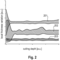
- FIG. 2 schematically exhibits the basic results of these measurements.
- FIG. 2 shows schematically three groups of results of different process conditions (201, 202 and 203) with respect to a localized thickness variation.
- the localized thickness variation (given in arbitrary units, a. u.) is plotted as a function of the cut in depth (in arbitrary units).
- FIG. 2 demonstrates that the three groups differ significantly both in an average level and in a local deviation from the local average.
- Each ingot piece was cut into a group of semiconductor wafers.
- Each group of semiconductor wafers then results in a band containing the values of the localized thickness change measurement as a function of cutting depth. Following the abscissa from left to right increases the depth of cut achieved.
- the first group 201 of wafers (cut from a first ingot piece) exhibits higher average localized thickness values as compared to the second group 202 and the third group 203.
- the wafers of the second group 202 exhibit a broader band of the localized thickness variation and the thickness of the band varies with increasing cutting depth.
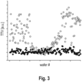
- FIG. 3 exhibits the result of the measurement of the total thickness variation (according to ASTM F657) of wafers taken from two different ingot pieces.
- Each TTV value is plotted against its wafer position (wafer #) in the corresponding ingot piece.
- the plot uses arbitrary units of measurements for simplicity and a qualitative comparison.
- the measurement of the first group of wafers 301 demonstrate significant scattering towards the ends of the crystal piece. Whereas, in the middle, the scattering and the average values appear rather low.
- the measurement of the second group of wafers 302 exhibits both, low values in TTV and at the same time low scattering between wafer and wafer which is very desirable.
- the inventors realized that, during the sawing process, both the location of the semiconductor wafer in the crystal piece and the respective depth of cut has an effect on the thickness variance (TTV) while using a diamond wire for cutting.
- TTV thickness variance
- FIG. 4 is a flow diagram of a method 400 according to an embodiment of the present invention.
- a semiconductor ingot is provided (S401).
- the semiconductor ingot is preferably a monocrystalline single crystal of silicon in the shape of a cylinder.
- the crystal After crystal growth, the crystal has a cone at each ends of the crystal which are typically cut off by using a band saw. Furthermore, the crystal shows surface undulations, which are caused by variations of thermal conditions during crystal growth. These undulations are eliminated by cylindrical grinding, resulting in a round cylinder with a smooth mantle surface.
- the semiconductor ingot (e.g., the monocrystalline silicon single crystal) is cut into a workpiece (e.g., a crystal workpiece) (S402).
- the workpiece e.g., the crystal workpiece
- the cut may be made by means of a saw (e.g., a band saw).
- the semiconductor ingot e.g., the single crystal
- workpieces e.g., crystal workpieces
- Wire saws are not capable of sawing very long ingots; and even if so (2) during crystal growth, quality parameters of the crystal change with increasing length. So, it is usually beneficial to select parts of the crystal for special customer needs.
- the workpiece e.g., crystal workpiece
- the workpiece is cut into slices (S403).
- the workpiece is cut by a wire grid (wire web or wire mesh).
- the wire grid may be composed of a fixed abrasive grain wire guided around two rollers containing grooves in which the sawing wire is guided.
- the workpiece e.g., the crystal workpiece
- a fixed abrasive grain wire can be understood as a wire where the abrasives are fixed on the surface of the wire.
- diamond wires are a variant of these class of sawing wires.
- a distance between two grooves on the roller is not less than 769 ⁇ m and not more than 850 ⁇ m.
- the initial cutting speed v start is preferably the highest value during the cut.
- v start is not less than 1.4 mm/min.
- the cutting speed during the cut is a function of the cutting depth following a parabolic line having the low point in the middle of the cut (half the diameter of the crystal piece) which has a value of 70% of v start .
- the coolant flow is set at the beginning of the cut to less than 0.1 l/h until a cutting depth of at least 7 mm and at most 13 mm is reached.
- the coolant flow is then set to a value of more than 2000 l/h, particularly preferably more than 2200 l/h.
- the coolant contains water and a surfactant. Most preferably, loose grains in the coolant are not intended to be used. The inventors realized that there are geometry issues at lower cutting depths than 7 mm and that there are issues still prevalent with TTV at higher cutting depth than 13 mm. This effect was present with both using a 70 ⁇ m and a 100 ⁇ m wire.
- the speed of the wire v w is to be set greater than 20 m/s while beginning with the cut.
- the direction of the wire speed is alternated during the cut and therefore it is preferred that the maximal speed is matched during the beginning of the cut.
- This method is also called crawl method and thus the length of the wire is called "pilgrim length".
- the maximum length of the wire traveling in one direction is more than 850 m before the direction is changed.
- the maximum length of the wire traveling in one direction is A graphic representation of this method can be seen in FIG. 5.
- Most preferably the minimum vocational length during the cut is not more than 98.5% of the initial pilgrim length.
- FIG. 5 shows the length of wire (in relative units) transported in one direction before the direction of the wire's speed is reversed. This method is also called mit method and thus the length of the wire is called "pilgrim length".
- the graph shows that this crawl length first decreases and then increases again with increasing depth of cut. In the graph the minimum vocational length is about 98% of the initial vocational length.
- the thickness of the sawing wire used is not more than 80 ⁇ m and not less than 60 ⁇ m.
- the recitation of "at least one of A, B and C” should be interpreted as one or more of a group of elements consisting of A, B and C, and should not be interpreted as requiring at least one of each of the listed elements A, B and C, regardless of whether A, B and C are related as categories or otherwise.
- the recitation of "A, B and/or C" or "at least one of A, B or C” should be interpreted as including any singular entity from the listed elements, e.g., A, any subset from the listed elements, e.g., A and B, or the entire list of elements A, B and C.
Landscapes
- Engineering & Computer Science (AREA)
- Mechanical Engineering (AREA)
- Processing Of Stones Or Stones Resemblance Materials (AREA)
- Mechanical Treatment Of Semiconductor (AREA)
- Finish Polishing, Edge Sharpening, And Grinding By Specific Grinding Devices (AREA)
- Grinding-Machine Dressing And Accessory Apparatuses (AREA)
- Polishing Bodies And Polishing Tools (AREA)
Claims (12)
- Verfahren zum Schneiden von Halbleiter-Wafern (301, 302), wobei das Verfahren Folgendes umfasst:Bereitstellen eines Halbleiter-Rohlings (101) in der Form eines Zylinders;Schneiden des Halbleiter-Rohlings in ein Werkstück unter Verwendung einer Säge; undSägen des Werkstücks in Scheiben unter Verwendung eines Drahtgitters (106), das einen Draht mit befestigten Schleifkörnern umfasst, der um zwei Walzen (102, 103) geführt ist, wobei die Walzen Nuten aufweisen, in denen der Draht mit befestigten Schleifkörnern geführt ist,wobei während des Sägens das Werkstück in Richtung des Drahtgitters (106) geführt wird, dadurch gekennzeichnet, dass bei einem ersten Kontakt des Werkstücks mit dem Drahtgitter (106) eine anfängliche Schneidgeschwindigkeit vstart kleiner als 2 mm/min ist, gleichzeitig eine Kühlmittelströmung kleiner als 0,1 l/h ist und gleichzeitig eine Geschwindigkeit vw des Drahts mit befestigten Schleifkörnern größer als 20 m/s ist,wobei nach einem ersten Kontakt das Werkstück durch das Drahtgitter geführt wird, bis eine erste Schneidtiefe von wenigstens 7 mm erreicht wird,wobei während des Sägens die Kühlmittelströmung konstant bleibt, bis die erste Schneidtiefe erreicht wird, und dann auf wenigstens 2000 l/h erhöht wird, undwobei die Schneidgeschwindigkeit zwischen dem ersten Kontakt des Werkstücks mit dem Drahtgitter und einer Schneidtiefe bis zu einem halben Durchmesser des Zylinders auf weniger als 70 % der anfänglichen Schneidgeschwindigkeit verringert wird und dann erhöht wird.
- Verfahren nach Anspruch 1, wobei die Halbleiter-Wafer (301, 302) Halbleiter-Wafer (301, 302) aus monokristallinem Silicium sind, wobei der Halbleiter-Rohling (101) ein monokristalliner Einkristall aus Silicium ist, wobei das Werkstück ein Kristallwerkstück mit einer Länge zwischen 350 mm und 450 mm ist und wobei die Säge eine Bandsäge ist.
- Verfahren nach Anspruch 2, wobei eine Dicke des Drahts mit befestigten Schleifkörnern nicht größer als 80 µm und nicht kleiner als 60 µm ist.
- Verfahren nach Anspruch 2, wobei der Draht mit befestigten Schleifkörnern einen Kerndraht umfasst und die Schleifkörner auf einer Oberfläche des Kerndrahts befestigt sind.
- Verfahren nach Anspruch 2, wobei die Kühlmittelströmung Wasser und einen oberflächenaktiven Stoff umfasst.
- Verfahren nach Anspruch 2, wobei die Nuten der Walzen (102, 103) einen Abstand zwischen einander von nicht kleiner als 769 µm und nicht größer als 850 µm aufweisen.
- Verfahren nach Anspruch 2, wobei eine Richtung des Drahtgitters (106) während des Schneidens abwechselt.
- Verfahren nach Anspruch 1, wobei der Draht mit befestigten Schleifkörnern ein Diamantdraht ist.
- Verfahren nach Anspruch 1, wobei die Schneidgeschwindigkeit während des Sägens eine Funktion der Schneidtiefe ist, die einer parabelförmigen Linie in einer Mitte des Schnitts folgt, die sich bei der Schneidtiefe eines halben Durchmessers des Zylinders befindet.
- Verfahren nach Anspruch 1, wobei die erste Schneidtiefe wenigstens 9 mm beträgt.
- Verfahren nach Anspruch 1, wobei die erste Schneidtiefe höchstens 13 mm beträgt.
- Verfahren nach Anspruch 1, wobei beim Erreichen der ersten Schneidtiefe die Kühlmittelströmung auf wenigstens 2200 l/h erhöht wird.
Applications Claiming Priority (2)
| Application Number | Priority Date | Filing Date | Title |
|---|---|---|---|
| US17/334,829 US11717930B2 (en) | 2021-05-31 | 2021-05-31 | Method for simultaneously cutting a plurality of disks from a workpiece |
| PCT/EP2022/063499 WO2022253578A1 (en) | 2021-05-31 | 2022-05-19 | Method for simultaneously cutting a plurality of disks from a workpiece |
Publications (2)
| Publication Number | Publication Date |
|---|---|
| EP4347207A1 EP4347207A1 (de) | 2024-04-10 |
| EP4347207B1 true EP4347207B1 (de) | 2025-04-30 |
Family
ID=82058325
Family Applications (1)
| Application Number | Title | Priority Date | Filing Date |
|---|---|---|---|
| EP22730406.0A Active EP4347207B1 (de) | 2021-05-31 | 2022-05-19 | Verfahren zum gleichzeitigen schneiden mehrerer scheiben von einem werkstück |
Country Status (7)
| Country | Link |
|---|---|
| US (1) | US11717930B2 (de) |
| EP (1) | EP4347207B1 (de) |
| JP (1) | JP7797541B2 (de) |
| KR (1) | KR102919620B1 (de) |
| CN (1) | CN117412847A (de) |
| TW (1) | TWI816414B (de) |
| WO (1) | WO2022253578A1 (de) |
Families Citing this family (3)
| Publication number | Priority date | Publication date | Assignee | Title |
|---|---|---|---|---|
| CN116001120B (zh) * | 2022-12-14 | 2024-08-13 | 山东有研半导体材料有限公司 | 一种半导体单晶硅片金刚线切割的工艺方法 |
| CN115958709B (zh) * | 2022-12-28 | 2023-06-20 | 宁波合盛新材料有限公司 | 碳化硅晶片的多线切割方法 |
| CN121223972B (zh) * | 2025-12-01 | 2026-03-17 | 晶科能源(海宁)有限公司 | 一种硅片切割方法、硅片和电池 |
Family Cites Families (32)
| Publication number | Priority date | Publication date | Assignee | Title |
|---|---|---|---|---|
| JPS60197361A (ja) * | 1984-03-19 | 1985-10-05 | Fujitsu Ltd | ワイヤ・スライシング方法 |
| DE19510625A1 (de) | 1995-03-23 | 1996-09-26 | Wacker Siltronic Halbleitermat | Drahtsäge und Verfahren zum Abtrennen von Scheiben von einem Werkstück |
| JP2891187B2 (ja) | 1995-06-22 | 1999-05-17 | 信越半導体株式会社 | ワイヤーソー装置及び切断方法 |
| JP3244426B2 (ja) | 1996-03-26 | 2002-01-07 | 信越半導体株式会社 | ワイヤソー用ワイヤの製造方法及びワイヤソー用ワイヤ |
| EP1287958A1 (de) * | 1996-03-26 | 2003-03-05 | Shin-Etsu Handotai Co., Ltd | Drahtsäge und Verfahren zum Zerschneiden eines zylindrischen Werkstücks |
| TW349041B (en) | 1996-11-08 | 1999-01-01 | Hitachi Cable | Wire for wire saw apparatus |
| JP3672146B2 (ja) * | 1997-03-27 | 2005-07-13 | 三菱住友シリコン株式会社 | ワイヤソーおよびインゴット切断方法 |
| US6279564B1 (en) | 1997-07-07 | 2001-08-28 | John B. Hodsden | Rocking apparatus and method for slicing a workpiece utilizing a diamond impregnated wire |
| US6652356B1 (en) * | 1999-01-20 | 2003-11-25 | Shin-Etsu Handotai Co., Ltd. | Wire saw and cutting method |
| JP2001334452A (ja) * | 2000-05-30 | 2001-12-04 | Memc Japan Ltd | 円柱状ワークの切断方法 |
| JP2002052456A (ja) * | 2001-07-06 | 2002-02-19 | Shin Etsu Chem Co Ltd | ウエーハの製造方法 |
| JP4791306B2 (ja) * | 2006-09-22 | 2011-10-12 | 信越半導体株式会社 | 切断方法 |
| JP4965949B2 (ja) * | 2006-09-22 | 2012-07-04 | 信越半導体株式会社 | 切断方法 |
| JP5430143B2 (ja) * | 2008-04-24 | 2014-02-26 | 京セラ株式会社 | 基板の製造方法 |
| JP5263536B2 (ja) * | 2009-07-14 | 2013-08-14 | 信越半導体株式会社 | ワークの切断方法 |
| US20110126813A1 (en) * | 2009-12-01 | 2011-06-02 | Diamond Wire Technology, Inc. | Multi-wire wafer cutting apparatus and method |
| DE102011008400B4 (de) * | 2011-01-12 | 2014-07-10 | Siltronic Ag | Verfahren zur Kühlung eines Werkstückes aus Halbleitermaterial beim Drahtsägen |
| JP2013004896A (ja) * | 2011-06-21 | 2013-01-07 | Nomura Micro Sci Co Ltd | 使用済み冷却液の回収方法及び回収装置 |
| DE102012201938B4 (de) * | 2012-02-09 | 2015-03-05 | Siltronic Ag | Verfahren zum gleichzeitigen Trennen einer Vielzahl von Scheiben von einem Werkstück |
| DE102012007815A1 (de) | 2012-04-18 | 2013-10-24 | Daimler Ag | Sägedraht und Verfahren zu dessen Herstellung |
| DE102012209974B4 (de) * | 2012-06-14 | 2018-02-15 | Siltronic Ag | Verfahren zum gleichzeitigen Abtrennen einer Vielzahl von Scheiben von einem zylindrischen Werkstück |
| JP5945967B2 (ja) * | 2013-06-27 | 2016-07-05 | 信越半導体株式会社 | ワークの切断方法及びワイヤソー |
| DE102014208187B4 (de) * | 2014-04-30 | 2023-07-06 | Siltronic Ag | Verfahren zum gleichzeitigen Trennen einer Vielzahl von Scheiben mit besonders gleichmäßiger Dicke von einem Werkstück |
| JP6172053B2 (ja) | 2014-05-28 | 2017-08-02 | 信越半導体株式会社 | 固定砥粒ワイヤ及びワイヤソー並びにワークの切断方法 |
| JP6589744B2 (ja) * | 2016-06-07 | 2019-10-16 | 株式会社Sumco | ワークの切断方法 |
| JP6642327B2 (ja) * | 2016-08-04 | 2020-02-05 | 株式会社Sumco | シリコンインゴットの切断方法およびシリコンウェーハの製造方法 |
| DE102016224640B4 (de) | 2016-12-09 | 2024-03-28 | Siltronic Ag | Verfahren zum Zersägen eines Werkstückes mit einer Drahtsäge |
| JP6617721B2 (ja) * | 2017-01-18 | 2019-12-11 | 信越半導体株式会社 | インゴット切断装置 |
| JP6693460B2 (ja) | 2017-04-04 | 2020-05-13 | 信越半導体株式会社 | ワークの切断方法 |
| DE102018218016A1 (de) | 2018-10-22 | 2020-04-23 | Siltronic Ag | Verfahren und Vorrichtung zum gleichzeitigen Trennen einer Vielzahl von Scheiben von einem Werkstück |
| DE102019207719A1 (de) | 2019-05-27 | 2020-12-03 | Siltronic Ag | Verfahren zum Abtrennen einer Vielzahl von Scheiben von Werkstücken während einer Anzahl von Abtrennvorgängen mittels einer Drahtsäge und Halbleiterscheibe aus einkristallinem Silizium |
| CN112297261B (zh) | 2019-07-29 | 2022-04-01 | 内蒙古中环光伏材料有限公司 | 一种太阳能用大尺寸硅片的切割工艺 |
-
2021
- 2021-05-31 US US17/334,829 patent/US11717930B2/en active Active
-
2022
- 2022-05-19 JP JP2023573645A patent/JP7797541B2/ja active Active
- 2022-05-19 CN CN202280038727.1A patent/CN117412847A/zh active Pending
- 2022-05-19 WO PCT/EP2022/063499 patent/WO2022253578A1/en not_active Ceased
- 2022-05-19 EP EP22730406.0A patent/EP4347207B1/de active Active
- 2022-05-19 KR KR1020237044190A patent/KR102919620B1/ko active Active
- 2022-05-31 TW TW111120282A patent/TWI816414B/zh active
Also Published As
| Publication number | Publication date |
|---|---|
| KR20240009511A (ko) | 2024-01-22 |
| JP7797541B2 (ja) | 2026-01-13 |
| TW202249109A (zh) | 2022-12-16 |
| KR102919620B1 (ko) | 2026-01-28 |
| WO2022253578A1 (en) | 2022-12-08 |
| JP2024522523A (ja) | 2024-06-21 |
| TWI816414B (zh) | 2023-09-21 |
| CN117412847A (zh) | 2024-01-16 |
| EP4347207A1 (de) | 2024-04-10 |
| US11717930B2 (en) | 2023-08-08 |
| US20220379426A1 (en) | 2022-12-01 |
Similar Documents
| Publication | Publication Date | Title |
|---|---|---|
| US9573296B2 (en) | Method for simultaneously cutting a multiplicity of slices of particularly uniform thickness from a workpiece | |
| US11717930B2 (en) | Method for simultaneously cutting a plurality of disks from a workpiece | |
| TWI556933B (zh) | 用於從工件同時切割多個晶圓的方法 | |
| JP5649692B2 (ja) | 円筒形の被加工物から多数のウェハを同時にスライスするための方法 | |
| US6832606B2 (en) | Wire saw and cutting method thereof | |
| JP6235295B2 (ja) | 固定砥粒ワイヤソー装置及びこれを用いたウエハの製造方法 | |
| JP7676567B2 (ja) | 半導体材料で作られた円筒状ロッドからディスクを製造する方法 | |
| JP5806082B2 (ja) | 被加工物の切断方法 | |
| JP2003165046A (ja) | ワイヤソー及び切断方法 | |
| KR102880759B1 (ko) | 공작물로부터 복수의 디스크를 동시에 분리하기 위한 방법 및 장치 | |
| JP5355249B2 (ja) | ワイヤーソー装置 | |
| Chandra et al. | Challenges in slicing large diameter silicon wafers using slurry wiresaw | |
| TW201304924A (zh) | 線切割裝置的主輪結構、其製作方法及線切割裝置 | |
| JP2004243509A (ja) | 砥粒含有繊維(ワイヤーソー)によるフラット面の加工方法 | |
| Watanabe et al. | Study of quartz crystal slicing technology by using unidirectional multi-wire-saw | |
| JPH09141647A (ja) | 内周刃ブレードの目立て方法 |
Legal Events
| Date | Code | Title | Description |
|---|---|---|---|
| STAA | Information on the status of an ep patent application or granted ep patent |
Free format text: STATUS: UNKNOWN |
|
| STAA | Information on the status of an ep patent application or granted ep patent |
Free format text: STATUS: THE INTERNATIONAL PUBLICATION HAS BEEN MADE |
|
| PUAI | Public reference made under article 153(3) epc to a published international application that has entered the european phase |
Free format text: ORIGINAL CODE: 0009012 |
|
| STAA | Information on the status of an ep patent application or granted ep patent |
Free format text: STATUS: REQUEST FOR EXAMINATION WAS MADE |
|
| 17P | Request for examination filed |
Effective date: 20231116 |
|
| AK | Designated contracting states |
Kind code of ref document: A1 Designated state(s): AL AT BE BG CH CY CZ DE DK EE ES FI FR GB GR HR HU IE IS IT LI LT LU LV MC MK MT NL NO PL PT RO RS SE SI SK SM TR |
|
| DAV | Request for validation of the european patent (deleted) | ||
| DAX | Request for extension of the european patent (deleted) | ||
| GRAP | Despatch of communication of intention to grant a patent |
Free format text: ORIGINAL CODE: EPIDOSNIGR1 |
|
| STAA | Information on the status of an ep patent application or granted ep patent |
Free format text: STATUS: GRANT OF PATENT IS INTENDED |
|
| INTG | Intention to grant announced |
Effective date: 20250116 |
|
| GRAS | Grant fee paid |
Free format text: ORIGINAL CODE: EPIDOSNIGR3 |
|
| GRAA | (expected) grant |
Free format text: ORIGINAL CODE: 0009210 |
|
| STAA | Information on the status of an ep patent application or granted ep patent |
Free format text: STATUS: THE PATENT HAS BEEN GRANTED |
|
| AK | Designated contracting states |
Kind code of ref document: B1 Designated state(s): AL AT BE BG CH CY CZ DE DK EE ES FI FR GB GR HR HU IE IS IT LI LT LU LV MC MK MT NL NO PL PT RO RS SE SI SK SM TR |
|
| REG | Reference to a national code |
Ref country code: CH Ref legal event code: EP Ref country code: GB Ref legal event code: FG4D |
|
| REG | Reference to a national code |
Ref country code: IE Ref legal event code: FG4D |
|
| REG | Reference to a national code |
Ref country code: DE Ref legal event code: R096 Ref document number: 602022013938 Country of ref document: DE |
|
| PGFP | Annual fee paid to national office [announced via postgrant information from national office to epo] |
Ref country code: DE Payment date: 20250521 Year of fee payment: 4 |
|
| PGFP | Annual fee paid to national office [announced via postgrant information from national office to epo] |
Ref country code: AT Payment date: 20250721 Year of fee payment: 4 |
|
| REG | Reference to a national code |
Ref country code: NL Ref legal event code: MP Effective date: 20250430 |
|
| REG | Reference to a national code |
Ref country code: AT Ref legal event code: MK05 Ref document number: 1789633 Country of ref document: AT Kind code of ref document: T Effective date: 20250430 |
|
| PG25 | Lapsed in a contracting state [announced via postgrant information from national office to epo] |
Ref country code: FI Free format text: LAPSE BECAUSE OF FAILURE TO SUBMIT A TRANSLATION OF THE DESCRIPTION OR TO PAY THE FEE WITHIN THE PRESCRIBED TIME-LIMIT Effective date: 20250430 Ref country code: ES Free format text: LAPSE BECAUSE OF FAILURE TO SUBMIT A TRANSLATION OF THE DESCRIPTION OR TO PAY THE FEE WITHIN THE PRESCRIBED TIME-LIMIT Effective date: 20250430 Ref country code: PT Free format text: LAPSE BECAUSE OF FAILURE TO SUBMIT A TRANSLATION OF THE DESCRIPTION OR TO PAY THE FEE WITHIN THE PRESCRIBED TIME-LIMIT Effective date: 20250901 |
|
| REG | Reference to a national code |
Ref country code: LT Ref legal event code: MG9D |
|
| PG25 | Lapsed in a contracting state [announced via postgrant information from national office to epo] |
Ref country code: GR Free format text: LAPSE BECAUSE OF FAILURE TO SUBMIT A TRANSLATION OF THE DESCRIPTION OR TO PAY THE FEE WITHIN THE PRESCRIBED TIME-LIMIT Effective date: 20250731 Ref country code: NO Free format text: LAPSE BECAUSE OF FAILURE TO SUBMIT A TRANSLATION OF THE DESCRIPTION OR TO PAY THE FEE WITHIN THE PRESCRIBED TIME-LIMIT Effective date: 20250730 |
|
| PG25 | Lapsed in a contracting state [announced via postgrant information from national office to epo] |
Ref country code: PL Free format text: LAPSE BECAUSE OF FAILURE TO SUBMIT A TRANSLATION OF THE DESCRIPTION OR TO PAY THE FEE WITHIN THE PRESCRIBED TIME-LIMIT Effective date: 20250430 Ref country code: NL Free format text: LAPSE BECAUSE OF FAILURE TO SUBMIT A TRANSLATION OF THE DESCRIPTION OR TO PAY THE FEE WITHIN THE PRESCRIBED TIME-LIMIT Effective date: 20250430 |
|
| PGFP | Annual fee paid to national office [announced via postgrant information from national office to epo] |
Ref country code: IT Payment date: 20250531 Year of fee payment: 4 |
|
| PG25 | Lapsed in a contracting state [announced via postgrant information from national office to epo] |
Ref country code: BG Free format text: LAPSE BECAUSE OF FAILURE TO SUBMIT A TRANSLATION OF THE DESCRIPTION OR TO PAY THE FEE WITHIN THE PRESCRIBED TIME-LIMIT Effective date: 20250430 |
|
| PG25 | Lapsed in a contracting state [announced via postgrant information from national office to epo] |
Ref country code: HR Free format text: LAPSE BECAUSE OF FAILURE TO SUBMIT A TRANSLATION OF THE DESCRIPTION OR TO PAY THE FEE WITHIN THE PRESCRIBED TIME-LIMIT Effective date: 20250430 Ref country code: AT Free format text: LAPSE BECAUSE OF FAILURE TO SUBMIT A TRANSLATION OF THE DESCRIPTION OR TO PAY THE FEE WITHIN THE PRESCRIBED TIME-LIMIT Effective date: 20250430 |
|
| PG25 | Lapsed in a contracting state [announced via postgrant information from national office to epo] |
Ref country code: RS Free format text: LAPSE BECAUSE OF FAILURE TO SUBMIT A TRANSLATION OF THE DESCRIPTION OR TO PAY THE FEE WITHIN THE PRESCRIBED TIME-LIMIT Effective date: 20250731 |
|
| PG25 | Lapsed in a contracting state [announced via postgrant information from national office to epo] |
Ref country code: IS Free format text: LAPSE BECAUSE OF FAILURE TO SUBMIT A TRANSLATION OF THE DESCRIPTION OR TO PAY THE FEE WITHIN THE PRESCRIBED TIME-LIMIT Effective date: 20250830 |
|
| PG25 | Lapsed in a contracting state [announced via postgrant information from national office to epo] |
Ref country code: LV Free format text: LAPSE BECAUSE OF FAILURE TO SUBMIT A TRANSLATION OF THE DESCRIPTION OR TO PAY THE FEE WITHIN THE PRESCRIBED TIME-LIMIT Effective date: 20250430 |
|
| REG | Reference to a national code |
Ref country code: CH Ref legal event code: H13 Free format text: ST27 STATUS EVENT CODE: U-0-0-H10-H13 (AS PROVIDED BY THE NATIONAL OFFICE) Effective date: 20251223 |
|
| PG25 | Lapsed in a contracting state [announced via postgrant information from national office to epo] |
Ref country code: DK Free format text: LAPSE BECAUSE OF FAILURE TO SUBMIT A TRANSLATION OF THE DESCRIPTION OR TO PAY THE FEE WITHIN THE PRESCRIBED TIME-LIMIT Effective date: 20250430 Ref country code: SM Free format text: LAPSE BECAUSE OF FAILURE TO SUBMIT A TRANSLATION OF THE DESCRIPTION OR TO PAY THE FEE WITHIN THE PRESCRIBED TIME-LIMIT Effective date: 20250430 |
|
| PG25 | Lapsed in a contracting state [announced via postgrant information from national office to epo] |
Ref country code: LU Free format text: LAPSE BECAUSE OF NON-PAYMENT OF DUE FEES Effective date: 20250519 |
|
| PG25 | Lapsed in a contracting state [announced via postgrant information from national office to epo] |
Ref country code: CH Free format text: LAPSE BECAUSE OF NON-PAYMENT OF DUE FEES Effective date: 20250531 |
|
| PG25 | Lapsed in a contracting state [announced via postgrant information from national office to epo] |
Ref country code: CZ Free format text: LAPSE BECAUSE OF FAILURE TO SUBMIT A TRANSLATION OF THE DESCRIPTION OR TO PAY THE FEE WITHIN THE PRESCRIBED TIME-LIMIT Effective date: 20250430 |
|
| PG25 | Lapsed in a contracting state [announced via postgrant information from national office to epo] |
Ref country code: EE Free format text: LAPSE BECAUSE OF FAILURE TO SUBMIT A TRANSLATION OF THE DESCRIPTION OR TO PAY THE FEE WITHIN THE PRESCRIBED TIME-LIMIT Effective date: 20250430 |
|
| PG25 | Lapsed in a contracting state [announced via postgrant information from national office to epo] |
Ref country code: SK Free format text: LAPSE BECAUSE OF FAILURE TO SUBMIT A TRANSLATION OF THE DESCRIPTION OR TO PAY THE FEE WITHIN THE PRESCRIBED TIME-LIMIT Effective date: 20250430 |
|
| REG | Reference to a national code |
Ref country code: BE Ref legal event code: MM Effective date: 20250531 |
|
| PG25 | Lapsed in a contracting state [announced via postgrant information from national office to epo] |
Ref country code: MC Free format text: LAPSE BECAUSE OF FAILURE TO SUBMIT A TRANSLATION OF THE DESCRIPTION OR TO PAY THE FEE WITHIN THE PRESCRIBED TIME-LIMIT Effective date: 20250430 |
|
| REG | Reference to a national code |
Ref country code: DE Ref legal event code: R097 Ref document number: 602022013938 Country of ref document: DE |
|
| PG25 | Lapsed in a contracting state [announced via postgrant information from national office to epo] |
Ref country code: RO Free format text: LAPSE BECAUSE OF FAILURE TO SUBMIT A TRANSLATION OF THE DESCRIPTION OR TO PAY THE FEE WITHIN THE PRESCRIBED TIME-LIMIT Effective date: 20250430 |
|
| PLBE | No opposition filed within time limit |
Free format text: ORIGINAL CODE: 0009261 |
|
| STAA | Information on the status of an ep patent application or granted ep patent |
Free format text: STATUS: NO OPPOSITION FILED WITHIN TIME LIMIT |
|
| REG | Reference to a national code |
Ref country code: CH Ref legal event code: L10 Free format text: ST27 STATUS EVENT CODE: U-0-0-L10-L00 (AS PROVIDED BY THE NATIONAL OFFICE) Effective date: 20260311 |
|
| 26N | No opposition filed |
Effective date: 20260202 |
|
| PG25 | Lapsed in a contracting state [announced via postgrant information from national office to epo] |
Ref country code: IE Free format text: LAPSE BECAUSE OF NON-PAYMENT OF DUE FEES Effective date: 20250519 |
|
| PG25 | Lapsed in a contracting state [announced via postgrant information from national office to epo] |
Ref country code: BE Free format text: LAPSE BECAUSE OF NON-PAYMENT OF DUE FEES Effective date: 20250531 |
|
| PG25 | Lapsed in a contracting state [announced via postgrant information from national office to epo] |
Ref country code: FR Free format text: LAPSE BECAUSE OF NON-PAYMENT OF DUE FEES Effective date: 20250630 |