EP4350302A2 - Appareil de détection de décroissance de fluorescence et ses procédés de fabrication - Google Patents
Appareil de détection de décroissance de fluorescence et ses procédés de fabrication Download PDFInfo
- Publication number
- EP4350302A2 EP4350302A2 EP24157394.8A EP24157394A EP4350302A2 EP 4350302 A2 EP4350302 A2 EP 4350302A2 EP 24157394 A EP24157394 A EP 24157394A EP 4350302 A2 EP4350302 A2 EP 4350302A2
- Authority
- EP
- European Patent Office
- Prior art keywords
- batch
- samples
- sensor
- phosphor powder
- fluorescent
- Prior art date
- Legal status (The legal status is an assumption and is not a legal conclusion. Google has not performed a legal analysis and makes no representation as to the accuracy of the status listed.)
- Pending
Links
Images


Classifications
-
- G—PHYSICS
- G01—MEASURING; TESTING
- G01K—MEASURING TEMPERATURE; MEASURING QUANTITY OF HEAT; THERMALLY-SENSITIVE ELEMENTS NOT OTHERWISE PROVIDED FOR
- G01K11/00—Measuring temperature based upon physical or chemical changes not covered by groups G01K3/00, G01K5/00, G01K7/00 or G01K9/00
- G01K11/32—Measuring temperature based upon physical or chemical changes not covered by groups G01K3/00, G01K5/00, G01K7/00 or G01K9/00 using changes in transmittance, scattering or luminescence in optical fibres
- G01K11/3206—Measuring temperature based upon physical or chemical changes not covered by groups G01K3/00, G01K5/00, G01K7/00 or G01K9/00 using changes in transmittance, scattering or luminescence in optical fibres at discrete locations in the fibre, e.g. using Bragg scattering
- G01K11/3213—Measuring temperature based upon physical or chemical changes not covered by groups G01K3/00, G01K5/00, G01K7/00 or G01K9/00 using changes in transmittance, scattering or luminescence in optical fibres at discrete locations in the fibre, e.g. using Bragg scattering using changes in luminescence, e.g. at the distal end of the fibres
-
- G—PHYSICS
- G01—MEASURING; TESTING
- G01D—MEASURING NOT SPECIALLY ADAPTED FOR A SPECIFIC VARIABLE; ARRANGEMENTS FOR MEASURING TWO OR MORE VARIABLES NOT COVERED IN A SINGLE OTHER SUBCLASS; TARIFF METERING APPARATUS; MEASURING OR TESTING NOT OTHERWISE PROVIDED FOR
- G01D5/00—Mechanical means for transferring the output of a sensing member; Means for converting the output of a sensing member to another variable where the form or nature of the sensing member does not constrain the means for converting; Transducers not specially adapted for a specific variable
- G01D5/26—Mechanical means for transferring the output of a sensing member; Means for converting the output of a sensing member to another variable where the form or nature of the sensing member does not constrain the means for converting; Transducers not specially adapted for a specific variable characterised by optical transfer means, i.e. using infrared, visible, or ultraviolet light
- G01D5/268—Mechanical means for transferring the output of a sensing member; Means for converting the output of a sensing member to another variable where the form or nature of the sensing member does not constrain the means for converting; Transducers not specially adapted for a specific variable characterised by optical transfer means, i.e. using infrared, visible, or ultraviolet light using optical fibres
-
- G—PHYSICS
- G01—MEASURING; TESTING
- G01K—MEASURING TEMPERATURE; MEASURING QUANTITY OF HEAT; THERMALLY-SENSITIVE ELEMENTS NOT OTHERWISE PROVIDED FOR
- G01K15/00—Testing or calibrating of thermometers
-
- B—PERFORMING OPERATIONS; TRANSPORTING
- B82—NANOTECHNOLOGY
- B82Y—SPECIFIC USES OR APPLICATIONS OF NANOSTRUCTURES; MEASUREMENT OR ANALYSIS OF NANOSTRUCTURES; MANUFACTURE OR TREATMENT OF NANOSTRUCTURES
- B82Y15/00—Nanotechnology for interacting, sensing or actuating, e.g. quantum dots as markers in protein assays or molecular motors
-
- B—PERFORMING OPERATIONS; TRANSPORTING
- B82—NANOTECHNOLOGY
- B82Y—SPECIFIC USES OR APPLICATIONS OF NANOSTRUCTURES; MEASUREMENT OR ANALYSIS OF NANOSTRUCTURES; MANUFACTURE OR TREATMENT OF NANOSTRUCTURES
- B82Y40/00—Manufacture or treatment of nanostructures
Definitions
- the present technology relates to a temperature probe capable of accurately sensing temperatures using a nanocomposite fluorescent material for use in phosphor thermometry. More specifically, it is a method of manufacturing a nanocomposite material that results in polycrystalline sensing elements and a fluorescence temperature sensor that includes the polycrystalline sensing element.
- Fluorescence can be very simply defined as the emission of light when a material is exposed to electromagnetic radiation. This emission may continue for a period of time after the initial excitation. The length of time that a material will emit is a product of several interactions that occur at the atomic level and the amount of energy that is absorbed. Both excitation and emission intensities behave exponentially with respect to time. This dual time-dependent behavior is a unique property that can be used to indicate the temperature of the fluorescent material.
- Fluorescent temperature sensors utilize the proportional relationship between the luminous time-decay of a phosphor and the temperature at which it is being held.
- an excitation light pulse is coupled into an optical fiber at one end and travels down the fiber and excites a fluorescent material at the other end.
- the excited light couples back into the same fiber and travels back toward the light source and is split off to a photodetector which produces an electrical signal that can be analyzed.
- the luminous intensity of the phosphor is thereby analyzed over a period of time and its time-decay constant is determined. This time-decay constant is then compared in a lookup table to known time-decay values for different reference temperatures. In this way, the time-decay is converted to temperature and the phosphor on the end of the fiber acts as the sensor element.
- Phosphor powders may be used for sensing temperature when affixed to the end of an optical fiber or attached to a target substrate. Phosphor powders in loose form, however, are unstable and unable to provide accurate temperature readings. The powders may be strengthened and stabilized by mixing them with a liquid binder, such as an epoxy before being applied to the end of an optical fiber and cured.
- a liquid binder such as an epoxy
- the binding of the phosphor powder in a solid matrix improves its stability with respect to hysteresis effects from thermal cycling and also protects the phosphor from external influences that may change over time such as the presence of moisture and various gas concentrations in the surrounding atmosphere which interact with the phosphor powder and affect its time-decay properties.
- a binder material to the phosphor powder works well in lower temperature regimes (below 250°C) because there are numerous optically transparent organic binder materials to choose from such as epoxy resins, silicones, and thermoplastics. At higher temperatures, however, these organic binders oxidize and contaminate the phosphor resulting in lower signal levels and a shift in time-decay response. It is therefore desirable to use an inorganic binder.
- Various liquid inorganic binders have been suggested including sodium silicate, HPC, LK, and ZAP manufactured by Zyp Coatings, Oak Ridge TN. While these materials can withstand higher temperatures, they all suffer from one or more of the following deficiencies:
- Various solid crystal fluorescent materials have been proposed for time-decay temperature sensing at high temperatures above 350 °C.
- Such crystals include Y 2 O 3 [yttria], Y 3 Al 5 O 12 [yttrium aluminum garnet or YAG], YAlO 3 [yttrium aluminum perovskite or YAP], and Al 2 O 3 [sapphire] doped with one or more rare earth element.
- a sensor may be fabricated from a YAG light guide with YAG-Er [erbium] grown on the end ( US Pat 6045259 ).
- YAG-Er Er
- One advantage of this type of sensor is its use for extreme temperature applications exceeding 700 °C.
- United States Patent 8,123,403 discloses a temperature sensor probe that can conduct stable measurements, and the manufacturing method of the same.
- the temperature sensor probe provides: a fluorescent material that is a mixture of a fluorescent substance and a transparent material; a thermosensitive part having a concave part in which the fluorescent material is arranged; a waveguide route rod that propagates excitation light, which is irradiated on the fluorescent material, and fluorescent light, which is produced by the fluorescent substance; and a protective tube that covers the side surfaces of the waveguide route rod.
- the fluorescent material is affixed to the tip of the waveguide route rod using the transparent material, and the waveguide route rod bites into the fluorescent material.
- the fluorescence sensor is not polycrystalline nor is it a solidified sintered sensor.
- the method does not include a step that would produce a polycrystalline sensor element.
- the disclosed sensor relies on a concave part to house a mixture of a fluorescent material and transparent material, and a waveguide route member that bites into the sensor material and an undescribed process of "sintering" to affix the waveguide to the fluorescent material.
- United States Patent 9,599,518 discloses a fiber optic temperature sensing system incorporating a thermal probe which utilizes a phosphor in the form of a microsphere.
- the microsphere is situated in air so as to produce a lensing effect in both coupling the excitation light delivered to it by the fiber and coupling the fluorescence produced by the phosphor microsphere back into the fiber.
- the thermal probe can be implemented in either a flexible or a rigid form.
- Materials for the phosphor microspheres include--but are not limited to--rare earth(s) doped single crystals, rare earth(s) doped ceramics, and ruby. When coupled to a suitable controller, these thermal probes can provide reliable temperature measurements even in environments characterized by strong electrical noise or electromagnetic interference.
- the fluorescence sensor is not sintered, nor is it polycrystalline nor is it a solidified sintered sensor.
- United States Patent 6,045,259 discloses a crystalline structure, comprising an optical waveguiding region, a crystalline fluorescent temperature sensing region, and a crystalline junction between the optical waveguiding region and the crystalline fluorescent temperature sensing region.
- An embodiment of the present invention is a novel fiber-optic temperature sensor functional under high-temperature conditions.
- the fiber-optic temperature sensor comprises a continuous crystalline fiber optic high temperature sensor probe having a crystalline optical waveguiding region with first and second ends, and a crystalline fluorescent temperature sensing tip at one end thereof.
- the crystalline optical waveguiding region and the crystalline fluorescent temperature sensing tip are preferably crystallographically and thermomechanically compatible with each other.
- the fluorescent temperature sensing tip contains fluorescent ions that can be excited to fluoresce and produce a fluorescence emission.
- the fiber optic high temperature sensor probe also contains a crystalline junction preferably having a continuous, crystalline structure throughout.
- the crystalline junction is located between, and attached to, the crystalline fluorescent temperature sensing tip and the first end of the crystalline optical waveguiding region such that, preferably, a continuous, crystalline fiber optic high temperature sensor probe is formed.
- the fluorescence sensor is not sintered, nor is it polycrystalline nor is it a solidified sintered sensor.
- United States Patent 9,537,047 discloses a method for fabricating an LED/phosphor structure where an array of blue light emitting diode (LED) dies are mounted on a submount wafer.
- a phosphor powder is mixed with an organic polymer filler, such as an acrylate or nitrocellulose.
- the liquid or paste mixture is then deposited over the LED dies or other substrate as a substantially uniform layer.
- the organic filler is then removed by being burned away in air or being subject to an O.sub.2 plasma process, or dissolved, leaving a porous layer of phosphor grains sintered together.
- the porous phosphor layer is impregnated with a sol-gel (e.g., a sol-gel of TEOS or MTMS) or liquid glass (e.g., sodium silicate or potassium silicate), also known as water glass, which saturates the porous structure.
- a sol-gel e.g., a sol-gel of TEOS or MTMS
- liquid glass e.g., sodium silicate or potassium silicate
- the fluorescence element is an LED phosphor coating. It is not polycrystalline nor is it a solidified sintered sensor. The method does not include a step that would produce a polycrystalline or solidified sintered sensor.
- United States Patent 9,434,876 discloses a phosphor-dispersed glass, including: a glass material; and a phosphor dispersed in the glass material, wherein the glass material is substantially free of Nb 2 O 5 and contains: 15 to 40 mass % of SiO 2 ; 10 to 30 mass % of B 2 O 3 ; 1 to 35 mass % of ZnO; 0 to 20 mass % of Al 2 O 3 ; 2 to 30 mass % in total of at least one kind selected from the group consisting of BaO, CaO and SrO; 0 to 1 mass % of MgO; 5 to 35 mass % in total of R 2 O (at least one selected from the group consisting of Li 2 O, Na 2 O and K 2 O); and 0 to 15 mass % in total of at least one of antimony oxide and tin oxide.
- the fluorescence sensor is not polycrystalline nor is it solidified sintered sensor. The method does not include a step that would produce a polycrystalline or solidified sintered sensor.
- United States Patent 4,652,143 discloses an optical temperature measurement technique that utilizes the decaying luminescent intensity characteristic of a sensor composed of a luminescent material that is excited to luminescence by a light pulse or other periodic or other intermittent source of radiation.
- the luminescent emissions of a preferred sensor exhibit an approximately exponential decay with time that is the average of a distribution of chemically reproducible crystallites and are repeatable with a high degree of accuracy regardless of excitation level or prior temperature history of the sensor.
- the fluorescence sensor is not sintered, nor is it polycrystalline nor is it a solidified sintered sensor.
- United States Patent 7,374,335 discloses a luminescent temperature sensor comprising (i) an object having a recess, (ii) a layer of luminescent material disposed in the recess, wherein the luminescent material emits electromagnetic radiation having a detectable optical characteristic that is functionally dependent on the temperature of the object, and (iii) a light waveguide in optical communication with the layer of luminescent material, is provided.
- a test device for measuring a temperature in a processing step comprising (i) an object having a surface and having a recess in the surface of the object, (ii) a layer of luminescent material disposed in the recess, wherein the luminescent material emits electromagnetic radiation having a detectable optical characteristic that is functionally dependent on the temperature of the object in response to a source of excitation radiation, and (iii) an optical window that seals said layer of luminescent material in the recess in the surface of the object, is provided.
- the fluorescence sensor is not sintered, nor is it polycrystalline nor is it a solidified sintered sensor.
- nanocomposite fluorescent material for higher temperature applications, a method of producing multiple sensor elements with substantially the same accuracy, and a method for adjusting a fluorescent material time-decay response. It would be preferable if the nanocomposite fluorescent material could be used in a high temperature fluorescent sensor and would improve the optical signal of the high temperature fluorescent sensor. Furthermore, it would be preferable if the nanocomposite fluorescent material was high density and was stable and accurate over time with minimal hysteresis in its time-decay versus temperature response.
- the present technology provides a method of manufacturing a nanocomposite fluorescent material for higher temperature applications, a method of producing multiple sensor elements with substantially the same accuracy and a method for adjusting a fluorescent material's time-decay response.
- the method utilizes high pressure prior to high temperature sintering to produce polycrystalline sensing elements.
- the polycrystalline nanocomposite fluorescent material can be used in a high temperature fluorescent sensor and improves the optical signal of the high temperature fluorescent sensor.
- the polycrystalline nanocomposite fluorescent material is high density and is stable and accurate over time with minimal hysteresis in its time-decay versus temperature response. It is also brighter and more stable with respect to time-decay at elevated temperatures and is therefore well suited as a sensor material for phosphor thermometry.
- a fluorescence sensor for use in phosphor thermometry, the sensor comprising: an optical light guide which includes a distal end; and a sensing element which includes a proximal end and an outer surface, the proximal end of the sensing element attached to the distal end or located proximate to the distal end, the sensing element comprising one of a monocrystalline solid, a polycrystalline solid or a polycrystalline nanocomposite.
- the fluorescence sensor the sensing element may be a nanocomposite with a solid density of greater than about 90% or is a polycrystalline solid with a solid density of greater than about 90%.
- the polycrystalline nanocomposite may include at least one host, at least one dopant and at least one filler.
- the sensing element may be attached to the distal end of the optical light guide.
- the fluorescence sensor may further comprise a glass bond between the distal end of the optical light guide and the sensing element.
- the optical light guide may be an optical fiber.
- the host may be at least one of YSO, YSZ, Y 2 O 3 , YVO 4 , YAG, YAP, YAM, YGG, Al 2 O 3 , La 2 O 2 S, Gd 2 O 2 S, Mg 2 TiO 4 , 3.5MgO 0.5MgF 2 GeO 2 , Mg 4 FGeO 6 and K 2 SiF 6 .
- the dopant may be at least one of Ce, Cr, Dy, Er, Eu, Gd, Ho, Mn, Nd, Pr, Sm, Tb, Ti and Yb.
- the filler may be at least one of silica, glass, borosilicate glass, diamond, and undoped host.
- the undoped host may be YSO, YSZ, Y 2 O 3 , YVO4, YAG, YGG, YAP, YAM, Al 2 O 3 , La 2 O 2 S, Gd 2 O 2 S, MgO, GeO 2 , TiO 2 , SiO 2 and MgF 2 .
- the filler may be silicon dioxide.
- the silicon dioxide concentration may be about 0.1% to 10% w/w.
- the silicon dioxide may be doped with at least one of Ce, Cr, Dy, Er, Eu, Gd, Ho, Mn, Nd, Pr, Sm, Tb, Ti and Yb.
- the fluorescence sensor may further comprise a protective sheath in which at least the sensing element is housed.
- polycrystalline nanocomposite for use in fluorescence time-decay sensing, the polycrystalline nanocomposite comprising a mixture of at least one host, at least one dopant and at least one filler.
- a polycrystalline nanocomposite for use in fluorescence time-decay sensing comprising a mixture of at least one host, at least one dopant and at least one filler, wherein the mixture is compacted under a high pressure of at least about 5 tons per square inch.
- the polycrystalline nanocomposite may be sintered.
- the host may be at least one of YSO, YSZ, Y 2 O 3 , YVO 4 , YAG, YAP, YAM, YGG, Al 2 O 3 , La 2 O 2 S, Gd 2 O 2 S, Mg 2 TiO 4 , 3.5MgO 0.5MgF 2 GeO 2 , Mg 4 FGeO 6 and K 2 SiF 6 .
- the dopant may be at least one of Ce, Cr, Dy, Er, Eu, Gd, Ho, Mn, Nd, Pr, Sm, Tb, Ti and Yb.
- the filler may be at least one of silica, glass, borosilicate glass, diamond and undoped host.
- the undoped host may be at least one of YSO, YSZ, Y 2 O 3 , YVO4, YAG, YGG, YAP, YAM, Al 2 O 3 , La 2 O 2 S, Gd 2 O 2 S, MgO, GeO 2 , TiO 2 , SiO 2 and MgF 2 .
- the filler may be silicon dioxide.
- the silicon dioxide concentration may be about 0.01% to 10% w/w.
- the silicon dioxide may be doped with at least one of Ce, Cr, Dy, Er, Eu, Gd, Ho, Mn, Nd, Pr, Sm, Tb, Ti and Yb.
- a method of manufacturing a polycrystalline nanocomposite fluorescent solid comprising:
- the at least one filler may be SiO 2 nanoparticles.
- the method may further comprise grinding the polycrystalline nanocomposite fluorescent solid into a powder of a substantially uniform particle size.
- the method may further comprise machining the polycrystalline nanocomposite fluorescent solid into sensing elements.
- a method of manufacturing a plurality of apparatuses by fine tuning the time-decay versus temperature response of a batch of fluorescent temperature sensor material comprising:
- the step of adjusting the batch materials may comprise adding one or more of the following materials to the batch:
- the optical light guide may comprise a bundle of optical fibers.
- the proximal end of the sensing element may be polished.
- the outer surface of the sensing element may be ground.
- the outer surface may be reflective surface.
- the fluorescence sensor may further comprise a sensor cap, the sensor cap housing the sensing element.
- the sensing element may be formed within the sensor cap or may be bonded to the sensor cap.
- the fluorescence sensor may further comprise a space between the distal end of the optical light guide and the proximal end of the sensing element, wherein the optical light guide is bonded to the sensor cap.
- the fluorescence sensor may further comprise a bond layer between the distal end of the optical light guide and the proximal end of the sensing element, the bond layer comprising at least one of silica, glass or silicate containing lithium, potassium or sodium.
- the protective sheath may have a similar coefficient of thermal expansion as the optical light guide.
- the protective sheath may be bonded to the optical light guide to define a cavity.
- the cavity may retain an inert gas or a vacuum.
- the sensing element may be coated with a coating of glass or silica or a silicate coating.
- the optical light guide may comprise one or more high numerical aperture optical fibers.
- the optical fibers may comprise a germanium doped silica core and a fluorosilica-doped silica cladding.
- the optical fibers may be heat formed into an unstressed shape with one or more bends.
- the present technology is directed to:
- a purpose of this method is to fine tune the time-decay versus temperature response of a batch of fluorescence sensor elements in accordance with the steps above.
- the present technology is also directed to a method of making the apparatus by bonding a sintered phosphor disc or crystal to the end of an optical fiber, retaining it in close intimate contact, and protecting it from the chemical environment.
- Phosphor powder - in the context of the present technology a phosphor powder is a combination of at least one host and at least one dopant, in other words, it is a doped host which absorbs energy from incident light at certain wavelengths and emits light at other wavelengths.
- Fluorescent material in the context of the present technology, fluorescent materials are comprised of phosphor powder(s) and filler(s).
- Fluorescence sensor element - in the context of the present technology a fluorescence sensor element is one of a monocrystalline solid, polycrystalline solid, or a polycrystalline nanocomposite of either a mixture of phosphor powder and glass or phosphor powder.
- Monocrystalline solid - in the context of the present technology a monocrystalline solid is a sintered fluorescent crystal of phosphor powder. It has grain sizes larger than about 100 microns, but typically understood to be without any grain boundaries. The monocrystalline solid ideally shall have greater than about 90% solid density.
- Polycrystalline solid - in the context of the present technology a polycrystalline solid is a sintered phosphor powder which results in a polycrystalline structure with grain sizes in the range of about 10 nanometers to about 100 microns.
- the polycrystalline solid ideally shall have greater than about 90% solid density.
- Polycrystalline nanocomposite - in the context of the present technology a polycrystalline nanocomposite is a sintered fluorescent material (phosphor powder and at least one filler) which results in a polycrystalline structure with grain sizes in the range of about 10 nanometers to about 100 microns.
- the polycrystalline nanocomposite ideally shall have greater than about 90% solid density.
- High Pressure in the context of the present technology, high pressure is at least about 5 tons per square inch, but preferably about 100 tons per square inch.
- Controlled atmosphere - in the context of the present technology, a controlled atmosphere is one of an inert gas atmosphere, an oxygen atmosphere or a vacuum.
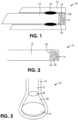
- Figure 1 shows an embodiment of a fluorescent temperature sensor for high temperature applications, generally referred to as 10. It includes an optical light guide 12 which may be a silica optical fiber, a sensing element 14 and a protective sheath 16, which preferably is opaque and does not need to be transparent.
- the protective sheath 16 is preferably a sealed end fused silica tube having the same or similar coefficient of thermal expansion as the optical light guide 12.
- the protective sheath is melt bonded at a melt bond 18 to the light guide 12 to define a cavity 15 in which at least the sensing element 14 is housed.
- the cavity 15 retains an inert gas or a vacuum.
- the sensing element 14 may have any shape, such as, but not limited to a small disc sized to fit on the distal end 20 of the optical light guide 12 at the proximal end 22 of the sensing element 14.
- the disc has a thickness of about 50 microns to about 1000 microns in order to maximize thermal conductivity through the disc, minimize thermal gradients across the disc, and maximize absorption and emission of the fluorescent signal.
- the sensing element 14 is a polycrystalline solid.
- the sensing element 14 is a polycrystalline nanocomposite.
- the sensing element 14 is capable of withstanding temperatures above about 350 degrees Celsius while producing a monotonic time-decay response with respect to temperature over a suitable range of temperatures.
- the cavity 15 creates a controlled environment for the sensing element which is desirable because at high temperatures oxidation occurs which can lead to dopant ion charge migration and hysteresis.
- the cavity 15 is very small (in the order of a few microns) hence there is no need to bond or otherwise attach the sensing element 14 to the optical light guide 12. This reduces the number of steps in manufacturing the fluorescent temperature sensor 10.
- the fluorescent temperature sensor 10 there is a glass bond layer 24 between the distal end 20 of the optical light guide 12 and the proximal end 22 of the sensing element 14.
- the glass bond material has a similar or lower melting temperature than the light guide 12 or sensor element 14 and aids in fusion of the distal end 20 of the optical light guide 12 to the proximal end 22 of the sensing element 14.
- This layer 24 may contain the same filler material used to create a polycrystalline nanocomposite sensing element 14 but can also be any solid, substantially transparent glass material that forms a mechanical bond between the sensing element 14 and optical light guide 12.
- Example glass bond layer 22 materials may include, but are not limited to borosilicate glass, specialty silica containing glass formulations, or a liquid glass such as potassium silicate, lithium silicate, sodium silicate or a combination thereof.
- the sensing element 14 has a larger diameter than the optical light guide 12.
- the distance between the distal end of the optical light guide 12 and the sensing element 14 and the diameter of the sensing element 14 are preferably calculated to match with the numerical aperture of the optical light guide 12 such that the cone of light emitted from the optical light guide 12 is focused on the sensor element 14.
- the sensing element 14 is a monocrystalline solid crystal and is affixed to the distal end 20 of the optical light guide 12 with or without a glass bond layer 24.
- the sensing element 14 may have a hemispherical shape as shown or a disc shape as shown in Figure 2 where the outer surface 32 of the sensing element 14 may be either polished or ground. Without being bound to theory, grinding the outer surfaces enhances back scattering of excitation light within the sensor element 14 thereby improving its absorption and emission intensity.
- a reflective surface coating 34 may also be applied to the outer surface 32 to help trap the light within the sensor element 14 and further improve its absorption and emission intensity.
- the distal end 20 of the optical light guide 12 has a polished surface 36.
- the proximal end 38 of the sensor element 22 also has a polished end.
- the protective sheath 16 can have a thinner end wall 40 for faster response time, but a larger thickness side wall 42 extending backwards which helps to protect the fragile optical light guide 12.
- the protective sheath 16 may be a glass such as fused silica, a ceramic such as alumina, or a metal such as Inconel ® .
- the protective sheath may be a polymer coating such as Teflon ® .
- a bundle 60 of smaller diameter optical fibers is used.
- the individual optical fibers 62 typically have a diameter in the range of about 40 microns to about 200 microns.
- a bundle 60 of borosilicate or silica optical fibers 62 may have a diameter of about 1000 microns and has a fused distal end 64 and the sensing element 14 affixed as discussed above.
- the bundle of optical fibers has the advantage of accommodating smaller bend radii while delivering more light to the sensing element 14 than a single optical fiber having the same minimum bend radius.
- a larger 1000 microns diameter optical fiber may be formed into a final shape with applicable bends. Heat is applied to the optical fiber and bends are made with a large enough radius to avoid light loss through the bends.
- the pre-forming step is done to reduce bending stress in the optical fiber which could result in breakage over time or if subject to rapid temperature change. In this case a higher numerical aperture optical fiber is also desired to accommodate smaller bend radii without signal loss.
- the light guide 12 is a heat-formed optical fiber with high numerical aperture (NA).
- NA numerical aperture
- Standard commercial grade silica optical fiber for high temperature applications has a typical NA of 0.22 which limits its light acceptance angle and limits its minimum bend radius.
- germanium doped silica core fiber where the NA is increased to about 0.37 or higher resulting in improved optical signal and smaller bend radii.
- the diameter of the optical fiber is about 200 microns to about 1000 microns and the germanium doped silica core is typically clad with a fluorosilica doped silica cladding 17. Heat forming the light guide followed by an annealing step allows complex bends to be formed, while eliminating the bending stresses which could lead to breakage in higher temperature applications.
- the sensing element 14 is attached to a sensing target 50 to be sensed and is illuminated by the light guide 12 some distance away from the target 50.
- the sensing target 50 may be individually tested for accuracy as part of the manufacturing process and prior to installation onto a surface 66 to be measured.
- a lens system 68 is located between the optical light guide 12 and the sensing element 14 which is bonded to an object 66.
- One or more optical lenses 68 may also be employed between the distal end of the optical light guide 12 and sensing element 14 to further extend the distance between the light guide 12 and sensing element 14 in remote sensing applications. In this way the temperature of the object 66 may be very high, but the lenses and optical light guide 12 may remain at much lower temperatures because they are located further away.
- the sensing element 14 is made of phosphor powder and at least one filler, which is pressed and sintered into a polycrystalline solid or polycrystalline nanocomposite, within the cap 72.
- caps 72 can be individually tested for accuracy before being assembled into a fluorescent temperature sensor 10.
- the distal region 70 can house an optical light guide 12 that is temporarily inserted during testing of the sensor cap.
- the sensing element 14 comprises a fluorescent polycrystalline solid or polycrystalline nanocomposite, material.
- the polycrystalline solid or polycrystalline nanocomposite contains host crystal material, a dopant, and a filler material.
- Table 1 shows examples of host crystals, dopants, and filler materials.
- the polycrystalline solid or polycrystalline nanocomposite material may contain any combination of host crystals, dopants, and filler materials, such as those listed in Table 1.
- the phosphor powder portion of the polycrystalline solid or polycrystalline nanocomposite material may contain any combination of any host crystal listed in Table 1 (or any other host crystal material known in the art) and one or more of the dopants listed in Table 1 (or any other dopants known in the art), for example YAG:Er and YAG:Nd.
- the filler material portion of the polycrystalline solid or polycrystalline nanocomposite may contain any of the filler materials listed Table 1 (or any filler material known in the art).
- the relative quantity of filler material with respect to the other materials may be about 0.1% to about 10% by weight of the total amount of materials.
- the particle shape of the filler material may be in the form of microspheres or randomly ground powder.
- the size of the particles may be from about 10 nanometers to about 10 microns.
- the filler material may be an un-doped host crystal as noted in Table 1. In another embodiment, the filler material may be a doped host crystal as noted in Table 1.
- specialty glass is a custom formulated glass with a lower melting point than the host crystal.
- filler material such as its thermal conductivity, its chemical compatibility with the doped host crystal, its susceptibility to oxidation and ion charge migration, its effect on time-decay response, and its useful operating temperature range.
- the filler material ideally is selected to be optically transparent in the excitation and absorption wavelengths of the doped host crystal.
- Another consideration is the chemical compatibility of the filler material with the operating environment into which the sensor may be deployed. Inertness is important because at high temperatures the host crystal may absorb gas molecules from the environment into its crystal lattice, thereby altering its time-decay response. The addition of a nanoparticle filler material in combination with high densification can significantly reduce this effect.
- ion charge migration may occur within the crystal lattice either as result of elevated temperatures or long-term exposure to incident light energy at specific wavelengths.
- the quantity of Er3+ versus Er2+ ions changes over temperature and with incident light intensity within a YAG crystal lattice. This changes the fluorescent time-decay response of the host crystal and leads to irreversible drift and hysteresis over time.
- an oxygen containing filler material is selected to provide additional oxygen ions to the crystal lattice and keep the Erbium in the Er3+ state.
- Table 1 Suitable Materials for Fluorescent Time-Decay Temperature Sensing Host Crystal Dopant (one or more) 0.1% to 20% Filler Material Particle Size: 10nm to 10 ⁇ m YSO Ce SiO 2 YSZ Cr Borosilicate Glass Y 2 O 3 Dy Specialty Glass* YVO 4 Er Diamond YAG Eu Undoped Host Crystal YAP Gd YSO YAM Ho YSZ YGG Mn Y 2 O 3 Al 2 O 3 Nd YVO 4 La 2 O 2 S Pr YAG Gd 2 O 2 S Sm YGG Mg 2 TiO 4 Tb YAP 3.5MgO 0.5MgF 2 GeO 2 Ti YAM Mg 4 FGeO 6 Tm Al 2 O 3 K 2 SiF 6 Yb La 2 O 2 S Gd 2 O 2 S MgO GeO 2 TiO 2 MgF 2 * Specialty glass formulations can be custom tailored for higher or lower melting points, clarity, and coefficients of thermal expansion to match the
- silicon dioxide is added at a concentration of about 0.1% to about 10% (see Table 2).
- the particle size is about 10 nanometers to about 10 microns.
- the addition of a small quantity of silicon dioxide to the crystal lattice of various phosphor powders or crystals serves to prevent ion charge migration within the crystal lattice, thus stabilizing its absorption and emission wavelengths and allowing its time-decay versus temperature response to be more accurate and repeatable.
- the silicon dioxide may be doped with at least one of Ce, Cr, Dy, Er, Eu, Gd, Ho, Mn, Nd, Pr, Sm, Tb, Ti and Yb to further enhance fluorescent efficiency.
- the sensor element 14 is a semi-transparent polycrystalline solid.
- the advantage of a polycrystalline solid over a monocrystalline solid is that grain boundaries in the polycrystalline structure help to trap light within the sensor which increases the absorption and emission intensity.
- the multiple grain boundaries may also help to distribute internal stresses, reduce ion charge migration and produce a more stable sensor element with less hysteresis.
- the method of producing a polycrystalline sensor element is as follows:
- Figure 10 shows a fluorescent sensor element 14 encapsulated with a glass coating 90 to protect it from external atmosphere.
- the glass coating 90 may be any glass including fused silica, borosilicate glass, or a silicate for example. Such a coating is applied to prevent chemical attack, oxidation, and humidity from affecting the fluorescent sensor element 14, and is particularly important if the sensor element is more porous and less dense.
- the fluorescent sensor element 14 may be used in any application where fluorescence time-decay is measured, for example, but not limited to pressure, oxygen, pH, or moisture sensing.
- the present technology is directed to a method of making multiple apparatus by fine tuning the time-decay versus temperature response of a batch of fluorescent sensor elements via the following steps:
- An objective of this method is to maximize the number of sensing elements produced that fall into a predetermined accuracy bin value.
- a large batch may be produced and thoroughly mixed. Small samples from this batch are then processed and tested and the batch is adjusted by means noted above until a majority of the test samples fall within the parameters of a particular accuracy bin.
- the sensing element may be manufactured in a variety of ways.
- Figure 11 illustrates disc shaped sensing elements 14 punched out of sheets 80 or cut from rods 81 of the sintered material.
- the sheets may have any desired thickness, for example from about 50 microns to about 1000 microns.
- the rods 81 may have any desired diameter, for example from about 200 microns to about 1000 microns.
- the step of solidifying the samples may be performed by baking, curing, drying or sintering, for example.
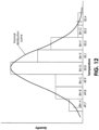
- the fluorescent sensor elements are sorted and binned according to their time-decay response versus temperature, as illustrated in Figure 12 . It is desirable to be able to sort and bin the resultant sensor elements 14 prior to full assembly with an optical light guide in order to improve yield and minimize the cost of scrap materials.
- the final batch of fluorescent material is deposited into a sensor cap or onto a target substrate and then solidified, hence the sensor element 14 is formed within the sensor cap.
- the method produces sensor elements after the original batch which have the same calibration accuracy as the original batch of sensor elements.
- each batch of bulk phosphor powder inevitably has slightly different time-decay versus temperature characteristics. This is undesirable because it means that fluorescent sensor elements produced with each new batch behave differently. For example, at a given temperature they may have a different time-decay than a previous batch and therefore must be calibrated differently. Calibrating individual sensors is inefficient and not practical. Therefore, a method is needed to adjust each new batch of bulk fluorescent material to match the performance characteristics from the previously produced batch.
- the method described below for fine tuning a batch of fluorescent material is used to correct batch-to-batch variability in the production of the bulk phosphor powder.
- a new batch can be fine-tuned to behave with the same fluorescent time-decay versus temperature characteristics as a previously produced batch. In this manner, sensors elements are produced over time with the same calibration accuracy as the original batch.
- a sensing element is manufactured in accordance with the following iterations of steps with the goal of maximizing the number of sensing elements produced that fall into bin D:
- Offset adjustments occur when the time-decay versus temperature response needs to be corrected in one direction and is a uniform offset applied across the entire temperature sensing range.
- Slope adjustment is required to correct for changes in time-decay versus temperature behavior over a range of temperatures where the offset at lower temperatures is different from the offset at higher temperatures.
- the filler material is commonly an inorganic transparent powder such as a glass or crystal material of similar or smaller particle size as the phosphor powder.
- both offset and slope can be corrected in order to match the current batch time-decay versus temperature characteristic to the original batch time-decay versus temperature characteristic.
- An objective of the method is to maximize the number of manufactured sensor elements 14 that fall into bin D. For example, after Sample Test 1, comparing the first test results with the predetermined accuracy bin value, a majority of sensing elements may fall in bin B and bin C. After adjustment and Sample Test 2, a majority of sensing elements may fall in bin C and bin D. After a final adjustment and Sample Test 3, a majority of sensing elements fall in the desired bin D.
- the sensor elements are discs. During the testing step, several discs are selected from the batch and tested to determine the statistical distribution of the batch.
- the method involves testing the samples in order to determine whether a majority of the samples would fall within the parameters of a predetermined accuracy bin value.
- an accuracy bin value may be 49.95 to 50.05 degrees Celsius.
- the samples may be tested by placing them in a precision drywell calibrator and setting the reference temperature to 50.00 degrees Celsius.
- a fiber optic light guide is placed in contact with each sample and its temperature is measured and recorded in a spreadsheet.
- a statistically meaningful number of samples are tested -- for example, a quantity of twenty sensor elements.
- a histogram is produced in the spreadsheet showing the temperature distribution of the samples. This distribution is typically gaussian in nature and will have a peak about which most of the samples read. This peak-value is then compared to the calibration reference temperature of 50.00 degrees Celsius. By subtracting the reference temperature from the gaussian peak temperature, an offset error value is determined. This offset error value is the offset that needs to be corrected through the batch adjustment process.
- Offset Example For example, in an embodiment, where the reference temperature is 50.00 degrees Celsius, if the Gaussian peak time-decay corresponds to a temperature of 49.50 degrees Celsius, then the batch would need to be adjusted to shift the temperature 0.5 degree Celsius higher. This adjustment may be accomplished in different ways, for example, by adding more phosphor material of the same type but with a smaller particle size distribution or by adding a filler material. If adding more phosphor powder of a different particle size, then the amount of material to be added is determined proportionally by the difference in temperature responses of the two batches. If a filler material is added, the amount is determined iteratively and through experience. It may take more than one iteration to adjust the batch to get the gaussian peak temperature to match the reference temperature.
- a second calibration point may be similarly tested at a higher temperature like 200.00 degrees Celsius. If the gaussian peak near 200.00 degrees Celsius shows an offset error different from the offset error determined at 50.00 degrees Celsius, then a slope adjustment must also be made. This may be accomplished by adding phosphor powder of the same type but of a different dopant concentration. The amount of material to be added is determined proportionally by the difference in slope characteristics of the two batches.
- Each bin of sorted sensor elements will have the same accuracy characteristics.
- the method manufactures multiple sensing elements from the same bin.
- the sensor elements may be mass produced in high volumes with repeatable fluorescent time-decay characteristics and maximum yield within the desired accuracy bin. This enables mass production of temperature probes with the desired accuracy.
- Figure 12 illustrates a histogram of grouped bins. If a high accuracy probe is desired, sensor elements from bin D are selected. If a lower accuracy is acceptable, sensor elements from the other bins may be selected.
- the method includes a step of adjusting the composition of the batch materials for adjusting the behavior of the fluorescent material matrix, which adjusts and corrects the time-decay reading from batch to batch (e.g. from Sample Test 1 to Sample Test 2), in two optional ways.
- the first option is by modifying the density and concentration of the fluorescent powder by adding a filler material to the powder.
- the second option is by introducing a second, phosphor powder of a different batch but similar chemical composition and adjusting its mix ratio with respect to the first phosphor powder.
- the composition of the batch materials is adjusted by modifying the density and concentration of the powder for example, by introducing an inorganic filler material of similar or smaller particle size to the phosphor powder.
- This option shifts the time-decay characteristics of the bulk matrix material.
- the higher the density the longer the time-decay and lower the temperature reading.
- adding 10% filler material may shift the temperature response higher by 0.2 to 2.0 degrees Celsius depending on phosphor powder.
- the inorganic filler may be a glass powder or a crystalline powder.
- Glass powders are acceptable for lower temperature operation, while crystalline powders are preferred for higher temperature operation. Examples of such materials are borosilicate glass, fused silica, diamond, YAG, and others.
- Second Option Adding a second batch of phosphor powder but with a different dopant concentration or particle size to the original phosphor powder
- the composition of the batch materials is adjusted by introducing a second phosphor powder of a different batch but similar chemical composition and adjusting its mix ratio with respect to the first batch phosphor powder.
- the second batch material may be made with an average particle size which is greater or lesser than the first batch. Larger particle size generally results in brighter, more efficient fluorescence and longer time-decay values and lower temperature readings.
- the second material may also be doped with a different dopant concentration.
- the concentration of Er can be adjusted from 0.1% to 20% by weight to shift the time-decay response.
- the method solidifies the samples and subsequently the entire batch by sintering the compacted powdered batch materials in controlled atmosphere environments for predetermined durations of time and within predetermined temperature ranges.
- the fluorescence sensing element is a phosphor powder-based sensor element that is sintered without the addition of a filler.
- a filler is added to a phosphor powder and mixed to provide a fluorescent material which is then compacted under high pressure into a green object having a solid, rigid shape.
- the green object is then sintered at high temperatures.
- the compacted fluorescent material may be sintered in a controlled atmosphere environment.
- doped YAG sintering may be performed in an inert nitrogen environment or in vacuum.
- sintering in air with oxygen present maximizes oxygen diffusion into the crystal and reduces the time needed for annealing.
- a fluorescent sensor object made from doped YAG may be sintered in a temperature range of about 1500 degrees Celsius to about 1900 degrees Celsius for about 2 to about 24 hours followed by annealing at a lower temperature range of about 800 degrees Celsius to about 1400 degrees Celsius for about 2 to about 48 hours.
- Annealing is ideally performed in air with oxygen present if the sensor is to operate in an air environment.
- annealing by cycling from about 800 degrees Celsius to about 1400 degrees Celsius over many hours or days will improve oxygen saturation and help stabilize ion charge migration which reduces time-decay hysteresis artifacts.
- the sintering time may be completed in as little as about 2 hours without need for further annealing.
- the addition of the filler thus also reduces the manufacturing processing time.
- the resultant final pressed and sintered product is ideally greater than 90% of the full monocrystalline solid density.
- the compacted powder object is sintered at predetermined temperature ranges and durations, which may vary depending on the powder materials. If the sintering time is prolonged, the grain structure will eventually form a monocrystalline solid. In some embodiments this may be desired because a solid crystal is very stable mechanically, however, in the case of materials such as rare-earth doped YAG, sintering to the point of an optically clear monocrystalline solid results in less fluorescent efficiency.
- the excitation light tends to travel through the crystal material with only a small fraction being absorbed in the crystal lattice. Sintering to a point of only polycrystalline grain structure increases fluorescent efficiency by providing better scattering and absorption of the excitation light resulting in thinner sensor element structures.
- rare earth doped YAG phosphor powder (without a filler) may be sintered into a solid structure and diced into a disc shape.
- the pressed shape of the solid structure can be a plate or a rod. Sintering can be done to partial polycrystalline formation or complete single crystal formation in the solid structure. The solid structure is then machined or diced into the desired sensor element shape (e.g. disc).
- the glass-phosphor powder matrix is mixed to provide a fluorescent material which is deposited and/or pressed under high pressure (at least about 5 tons per square inch) (compacted) into a cap or onto a target substrate.
- the high temperature sintering and annealing process is then conducted on the cap or target assembly.
- the sintered material also forms a mechanical bond with the cap or the target substrate.
- the filler material is added to lower the sintering temperature of the mixture.
- lower melting temperature glass powders with melting points around 700°C may be used with magnesium fluorogermanate phosphors to produce fluorescent sensor elements with working temperatures up to 600°C.
- filler powder particle size is similar in size or smaller than the phosphor particle size.
- Nanoparticle fillers and nanoparticle phosphors may be used.
- the fluorescent temperature sensor 10 is part of a phosphor thermometry apparatus, generally referred to as 100. It includes a light source 102, a light detector 104, which may be for example, but not limited to a photodetector, an analogue to digital converter 106, a printed circuit board 108, which includes a microprocessor 110 and a memory 112.
- the memory 112 has instructions thereon to instruct the processor to determine temperature based on the optical signal from the fluorescent sensor element, which is then transmitted from the printed circuit board 108 as an electronic digital signal.
Landscapes
- Physics & Mathematics (AREA)
- General Physics & Mathematics (AREA)
- Luminescent Compositions (AREA)
- Investigating, Analyzing Materials By Fluorescence Or Luminescence (AREA)
- Measuring Temperature Or Quantity Of Heat (AREA)
- Radiation Pyrometers (AREA)
Applications Claiming Priority (3)
| Application Number | Priority Date | Filing Date | Title |
|---|---|---|---|
| US201962812843P | 2019-03-01 | 2019-03-01 | |
| EP20766222.2A EP3931537A4 (fr) | 2019-03-01 | 2020-01-21 | Appareil de détection de déclin du temps de fluorescence et ses procédés de fabrication |
| PCT/CA2020/000004 WO2020176964A1 (fr) | 2019-03-01 | 2020-01-21 | Appareil de détection de déclin du temps de fluorescence et ses procédés de fabrication |
Related Parent Applications (1)
| Application Number | Title | Priority Date | Filing Date |
|---|---|---|---|
| EP20766222.2A Division EP3931537A4 (fr) | 2019-03-01 | 2020-01-21 | Appareil de détection de déclin du temps de fluorescence et ses procédés de fabrication |
Publications (2)
| Publication Number | Publication Date |
|---|---|
| EP4350302A2 true EP4350302A2 (fr) | 2024-04-10 |
| EP4350302A3 EP4350302A3 (fr) | 2024-07-17 |
Family
ID=72337390
Family Applications (3)
| Application Number | Title | Priority Date | Filing Date |
|---|---|---|---|
| EP24157392.2A Pending EP4350301A3 (fr) | 2019-03-01 | 2020-01-21 | Appareil de détection de décroissance de fluorescence et ses procédés de fabrication |
| EP20766222.2A Pending EP3931537A4 (fr) | 2019-03-01 | 2020-01-21 | Appareil de détection de déclin du temps de fluorescence et ses procédés de fabrication |
| EP24157394.8A Pending EP4350302A3 (fr) | 2019-03-01 | 2020-01-21 | Appareil de détection de décroissance de fluorescence et ses procédés de fabrication |
Family Applications Before (2)
| Application Number | Title | Priority Date | Filing Date |
|---|---|---|---|
| EP24157392.2A Pending EP4350301A3 (fr) | 2019-03-01 | 2020-01-21 | Appareil de détection de décroissance de fluorescence et ses procédés de fabrication |
| EP20766222.2A Pending EP3931537A4 (fr) | 2019-03-01 | 2020-01-21 | Appareil de détection de déclin du temps de fluorescence et ses procédés de fabrication |
Country Status (5)
| Country | Link |
|---|---|
| US (3) | US20220163405A1 (fr) |
| EP (3) | EP4350301A3 (fr) |
| JP (2) | JP2022522165A (fr) |
| KR (1) | KR20210133281A (fr) |
| WO (1) | WO2020176964A1 (fr) |
Families Citing this family (7)
| Publication number | Priority date | Publication date | Assignee | Title |
|---|---|---|---|---|
| US20200398305A1 (en) * | 2019-06-18 | 2020-12-24 | National Technology & Engineering Solutions Of Sandia, Llc | Aerosol Deposition of Thermographic Phosphor Coatings |
| US12104933B2 (en) * | 2019-06-25 | 2024-10-01 | Nagano Keiki Co., Ltd. | Optical sensor and physical quantity measurement device |
| CN113390529B (zh) * | 2021-06-10 | 2023-10-27 | 松山湖材料实验室 | 适于超宽测温范围的荧光测温方法 |
| CN118647687A (zh) * | 2022-01-28 | 2024-09-13 | 株式会社东芝 | 蓄冷材料、蓄冷材料粒子、造粒粒子、蓄冷器、冷冻机、低温泵、超导磁铁、核磁共振成像装置、核磁共振装置、磁场施加式单晶提拉装置、氦再冷凝装置及稀释冷冻机 |
| WO2026058834A1 (fr) | 2024-09-10 | 2026-03-19 | Sanyo Trading Co., Ltd. | Procédé de production d'une couche de tissu gaufré |
| CN119394464B (zh) * | 2024-10-28 | 2025-08-15 | 河北大学 | 一种基于Sm离子/Tb离子发光的比值温度传感方法 |
| CN121230907A (zh) * | 2025-11-07 | 2025-12-30 | 中绿中科储能技术有限公司 | 一种用于换热器内部流道的测温方法与装置 |
Citations (7)
| Publication number | Priority date | Publication date | Assignee | Title |
|---|---|---|---|---|
| US4652143A (en) | 1984-11-29 | 1987-03-24 | Luxtron Corporation | Optical temperature measurement techniques |
| US6045259A (en) | 1996-10-04 | 2000-04-04 | University Of South Florida | Fiber-optic high temperature sensor |
| US7374335B2 (en) | 2001-04-20 | 2008-05-20 | Luxtron Corporation | In situ optical surface temperature measuring techniques and devices |
| US8123403B2 (en) | 2007-11-22 | 2012-02-28 | Yamatake Corporation | Temperature sensor probe and manufacturing method of the same |
| US9434876B2 (en) | 2014-10-23 | 2016-09-06 | Central Glass Company, Limited | Phosphor-dispersed glass |
| US9537047B2 (en) | 2012-03-29 | 2017-01-03 | Koninklijke Philips N.V. | Phosphor in inorganic binder for LED applications |
| US9599518B2 (en) | 2013-01-29 | 2017-03-21 | Nicholas I. Djeu | Fiber optic temperature sensor utilizing a phosphor microsphere |
Family Cites Families (15)
| Publication number | Priority date | Publication date | Assignee | Title |
|---|---|---|---|---|
| DE3202089C2 (de) * | 1982-01-23 | 1985-01-17 | Fa. Carl Zeiss, 7920 Heidenheim | Faseroptischer Temperatursensor |
| US4788163A (en) * | 1987-08-20 | 1988-11-29 | General Electric Company | Devitrifying glass frits |
| US5414266A (en) * | 1993-06-11 | 1995-05-09 | Luxtron Corporation | Measuring system employing a luminescent sensor and methods of designing the system |
| US6048911A (en) * | 1997-12-12 | 2000-04-11 | Borden Chemical, Inc. | Coated optical fibers |
| CA2618685C (fr) * | 2005-08-12 | 2015-02-03 | Fiso Technologies Inc. | Capteur optique de fabry-perot constitue d'une seule piece et procede de fabrication de celui-ci |
| US20080069180A1 (en) * | 2006-09-19 | 2008-03-20 | Derek Djeu | Fiber optic temperature sensing system using a hemispherical phosphor |
| JP5001119B2 (ja) * | 2007-11-22 | 2012-08-15 | アズビル株式会社 | 温度センサプローブ、及びその製造方法 |
| US20100247893A1 (en) * | 2009-03-25 | 2010-09-30 | Goldeneye, Inc. | High quality luminescent materials for solid state lighting applications |
| JP5775722B2 (ja) * | 2011-03-31 | 2015-09-09 | 株式会社スミテック | 蛍光温度計及び温度計測方法 |
| CN102297733A (zh) * | 2011-05-27 | 2011-12-28 | 浙江大学 | 一种单晶光纤荧光温度传感器探头及其制备方法 |
| WO2015135888A1 (fr) * | 2014-03-13 | 2015-09-17 | Koninklijke Philips N.V. | Luminophore supertétraédrique pour un éclairage à l'état solide |
| JP6296958B2 (ja) * | 2014-10-15 | 2018-03-20 | アズビル株式会社 | 蛍光温度センサ |
| WO2016098586A1 (fr) * | 2014-12-18 | 2016-06-23 | 安立計器株式会社 | Procédé de fabrication d'un thermomètre à fibres optiques fluorescentes, et thermomètre à fibres optiques fluorescentes |
| US10222274B2 (en) * | 2016-09-28 | 2019-03-05 | General Electric Company | Thermographic temperature sensor |
| US20190187003A1 (en) * | 2017-12-14 | 2019-06-20 | Lam Research Corporation | Corrosion-Resistant Temperature Sensor Probe |
-
2020
- 2020-01-21 EP EP24157392.2A patent/EP4350301A3/fr active Pending
- 2020-01-21 US US17/433,015 patent/US20220163405A1/en active Pending
- 2020-01-21 JP JP2021549900A patent/JP2022522165A/ja active Pending
- 2020-01-21 KR KR1020217031339A patent/KR20210133281A/ko active Pending
- 2020-01-21 EP EP20766222.2A patent/EP3931537A4/fr active Pending
- 2020-01-21 WO PCT/CA2020/000004 patent/WO2020176964A1/fr not_active Ceased
- 2020-01-21 EP EP24157394.8A patent/EP4350302A3/fr active Pending
-
2024
- 2024-02-29 US US18/591,650 patent/US20240247984A1/en active Pending
- 2024-02-29 US US18/591,632 patent/US20240344899A1/en active Pending
- 2024-08-05 JP JP2024128847A patent/JP2024156892A/ja active Pending
Patent Citations (7)
| Publication number | Priority date | Publication date | Assignee | Title |
|---|---|---|---|---|
| US4652143A (en) | 1984-11-29 | 1987-03-24 | Luxtron Corporation | Optical temperature measurement techniques |
| US6045259A (en) | 1996-10-04 | 2000-04-04 | University Of South Florida | Fiber-optic high temperature sensor |
| US7374335B2 (en) | 2001-04-20 | 2008-05-20 | Luxtron Corporation | In situ optical surface temperature measuring techniques and devices |
| US8123403B2 (en) | 2007-11-22 | 2012-02-28 | Yamatake Corporation | Temperature sensor probe and manufacturing method of the same |
| US9537047B2 (en) | 2012-03-29 | 2017-01-03 | Koninklijke Philips N.V. | Phosphor in inorganic binder for LED applications |
| US9599518B2 (en) | 2013-01-29 | 2017-03-21 | Nicholas I. Djeu | Fiber optic temperature sensor utilizing a phosphor microsphere |
| US9434876B2 (en) | 2014-10-23 | 2016-09-06 | Central Glass Company, Limited | Phosphor-dispersed glass |
Non-Patent Citations (2)
| Title |
|---|
| OGI ET AL., ECS JOURNAL OF SOLID STATE SCIENCE AND TECHNOLOGY, vol. 2, no. 5, 2013, pages R91 - R95 |
| OPTICAL MATERIALS, vol. 75, pages 814 - 820 |
Also Published As
| Publication number | Publication date |
|---|---|
| WO2020176964A1 (fr) | 2020-09-10 |
| EP4350301A3 (fr) | 2024-07-10 |
| JP2022522165A (ja) | 2022-04-14 |
| EP4350301A2 (fr) | 2024-04-10 |
| EP4350302A3 (fr) | 2024-07-17 |
| JP2024156892A (ja) | 2024-11-06 |
| KR20210133281A (ko) | 2021-11-05 |
| EP3931537A1 (fr) | 2022-01-05 |
| US20240247984A1 (en) | 2024-07-25 |
| US20240344899A1 (en) | 2024-10-17 |
| US20220163405A1 (en) | 2022-05-26 |
| EP3931537A4 (fr) | 2023-02-22 |
Similar Documents
| Publication | Publication Date | Title |
|---|---|---|
| US20240344899A1 (en) | Fluorescence time decay sensing apparatus and methods of manufacturing same | |
| EP1689916B1 (fr) | Substances de scintillation (variantes) | |
| US7132060B2 (en) | Scintillation substances (variants) | |
| Yusoff et al. | Review of development of a silica-based thermoluminescence dosimeter | |
| JP6033879B2 (ja) | 発光物質、及び発光物質を形成するためのプロセス | |
| JP2957622B2 (ja) | 蛍光材を使用した温度測定法並びに蛍光材の製造方法 | |
| US20080017802A1 (en) | Fluorescent Material, a Method of Manufacturing the Fluorescent Material, a Radiation Detector Using the Fluorescent Material, and an X-Ray Ct Scanner | |
| US7666818B2 (en) | Combinatorial synthesis of ceramic materials | |
| Sun et al. | A highly robust Ce 3+-doped and Gd 3+-mixed KLaF 4 nano-glass composite scintillator | |
| Aizawa et al. | Fluorescence thermometer based on the photoluminescence intensity ratio in Tb doped phosphor materials | |
| JP5652904B2 (ja) | 中性子シンチレータ用酸化物結晶及びこれを用いた中性子シンチレータ | |
| Li et al. | Fluorescent optical fiber intensity ratio temperature sensor based on polymer matrix using down-conversion from ZnS: Cu | |
| WANG et al. | Large-size Er, Yb: YAG single crystal: growth and performance | |
| CN110760307B (zh) | 一种稀土掺杂石榴石结构闪烁体 | |
| Wang et al. | Effects of Er3+ doping on the structure and electro-optical properties of 0.94 (K0. 5Na0. 5) NbO3–0.06 Sr (Zn1/3Nb2/3) O3 ceramics | |
| JP5842292B2 (ja) | 中性子シンチレータ用酸化物結晶及びこれを用いた中性子シンチレータ | |
| JP2020075958A (ja) | Lso系シンチレータ結晶 | |
| CN118165731A (zh) | 一种上转换柔性荧光光纤及软包电池实时温度监控装置 | |
| CN121975523A (en) | High-energy-resolution garnet aluminate scintillation material and preparation method and application thereof | |
| Woody et al. | Fast Dense Low cost Scintillator for Nuclear Physics | |
| CN117848539A (zh) | 一种基于稀土掺杂铝酸盐多晶的温度传感器探头及其制备方法 | |
| CZ37255U1 (cs) | Multikomponentní monokrystalický scintilátor | |
| CN118480351A (zh) | 八面体格位掺杂改善铝镓酸钆闪烁材料、制备方法和应用 | |
| CN120967489A (zh) | 一种垂直梯度冷凝法生长碳镁共掺蓝宝石晶体的方法 | |
| Pracka et al. | Czochralski growth and characterization of SrLaGa3O7: Ho3+ single crystals |
Legal Events
| Date | Code | Title | Description |
|---|---|---|---|
| PUAI | Public reference made under article 153(3) epc to a published international application that has entered the european phase |
Free format text: ORIGINAL CODE: 0009012 |
|
| STAA | Information on the status of an ep patent application or granted ep patent |
Free format text: STATUS: THE APPLICATION HAS BEEN PUBLISHED |
|
| AC | Divisional application: reference to earlier application |
Ref document number: 3931537 Country of ref document: EP Kind code of ref document: P |
|
| AK | Designated contracting states |
Kind code of ref document: A2 Designated state(s): AL AT BE BG CH CY CZ DE DK EE ES FI FR GB GR HR HU IE IS IT LI LT LU LV MC MK MT NL NO PL PT RO RS SE SI SK SM TR |
|
| REG | Reference to a national code |
Ref country code: DE Ref legal event code: R079 Free format text: PREVIOUS MAIN CLASS: G01D0005260000 Ipc: G01K0011321300 |
|
| PUAL | Search report despatched |
Free format text: ORIGINAL CODE: 0009013 |
|
| AK | Designated contracting states |
Kind code of ref document: A3 Designated state(s): AL AT BE BG CH CY CZ DE DK EE ES FI FR GB GR HR HU IE IS IT LI LT LU LV MC MK MT NL NO PL PT RO RS SE SI SK SM TR |
|
| RIC1 | Information provided on ipc code assigned before grant |
Ipc: G01K 15/00 20060101ALI20240607BHEP Ipc: G01D 5/26 20060101ALI20240607BHEP Ipc: G01K 11/3213 20210101AFI20240607BHEP |
|
| RAP3 | Party data changed (applicant data changed or rights of an application transferred) |
Owner name: REEVES, NICHOLAS Owner name: BALAJI, SHARADA Owner name: JAMES, DARYL |
|
| RIN1 | Information on inventor provided before grant (corrected) |
Inventor name: REEVES, NICHOLAS Inventor name: BALAJI, SHARADA Inventor name: JAMES, DARYL |
|
| STAA | Information on the status of an ep patent application or granted ep patent |
Free format text: STATUS: REQUEST FOR EXAMINATION WAS MADE |
|
| 17P | Request for examination filed |
Effective date: 20250107 |
|
| STAA | Information on the status of an ep patent application or granted ep patent |
Free format text: STATUS: EXAMINATION IS IN PROGRESS |
|
| 17Q | First examination report despatched |
Effective date: 20260325 |