EP4350723B1 - Halbleiterchip mit transformator und esd-klemmschaltung - Google Patents
Halbleiterchip mit transformator und esd-klemmschaltung Download PDFInfo
- Publication number
- EP4350723B1 EP4350723B1 EP23194376.2A EP23194376A EP4350723B1 EP 4350723 B1 EP4350723 B1 EP 4350723B1 EP 23194376 A EP23194376 A EP 23194376A EP 4350723 B1 EP4350723 B1 EP 4350723B1
- Authority
- EP
- European Patent Office
- Prior art keywords
- terminal
- esd
- electrically coupled
- winding
- die
- Prior art date
- Legal status (The legal status is an assumption and is not a legal conclusion. Google has not performed a legal analysis and makes no representation as to the accuracy of the status listed.)
- Active
Links
Images


Classifications
-
- H—ELECTRICITY
- H02—GENERATION; CONVERSION OR DISTRIBUTION OF ELECTRIC POWER
- H02H—EMERGENCY PROTECTIVE CIRCUIT ARRANGEMENTS
- H02H9/00—Emergency protective circuit arrangements for limiting excess current or voltage without disconnection
- H02H9/04—Emergency protective circuit arrangements for limiting excess current or voltage without disconnection responsive to excess voltage
- H02H9/045—Emergency protective circuit arrangements for limiting excess current or voltage without disconnection responsive to excess voltage adapted to a particular application and not provided for elsewhere
- H02H9/046—Emergency protective circuit arrangements for limiting excess current or voltage without disconnection responsive to excess voltage adapted to a particular application and not provided for elsewhere responsive to excess voltage appearing at terminals of integrated circuits
-
- H—ELECTRICITY
- H01—ELECTRIC ELEMENTS
- H01F—MAGNETS; INDUCTANCES; TRANSFORMERS; SELECTION OF MATERIALS FOR THEIR MAGNETIC PROPERTIES
- H01F27/00—Details of transformers or inductances, in general
- H01F27/40—Structural association with built-in electric component, e.g. fuse
- H01F27/402—Association of measuring or protective means
-
- H—ELECTRICITY
- H02—GENERATION; CONVERSION OR DISTRIBUTION OF ELECTRIC POWER
- H02H—EMERGENCY PROTECTIVE CIRCUIT ARRANGEMENTS
- H02H9/00—Emergency protective circuit arrangements for limiting excess current or voltage without disconnection
-
- H—ELECTRICITY
- H01—ELECTRIC ELEMENTS
- H01F—MAGNETS; INDUCTANCES; TRANSFORMERS; SELECTION OF MATERIALS FOR THEIR MAGNETIC PROPERTIES
- H01F27/00—Details of transformers or inductances, in general
- H01F27/28—Coils; Windings; Conductive connections
-
- H—ELECTRICITY
- H02—GENERATION; CONVERSION OR DISTRIBUTION OF ELECTRIC POWER
- H02H—EMERGENCY PROTECTIVE CIRCUIT ARRANGEMENTS
- H02H9/00—Emergency protective circuit arrangements for limiting excess current or voltage without disconnection
- H02H9/04—Emergency protective circuit arrangements for limiting excess current or voltage without disconnection responsive to excess voltage
- H02H9/045—Emergency protective circuit arrangements for limiting excess current or voltage without disconnection responsive to excess voltage adapted to a particular application and not provided for elsewhere
- H02H9/047—Free-wheeling circuits
-
- H—ELECTRICITY
- H03—ELECTRONIC CIRCUITRY
- H03F—AMPLIFIERS
- H03F1/00—Details of amplifiers with only discharge tubes, only semiconductor devices or only unspecified devices as amplifying elements
- H03F1/52—Circuit arrangements for protecting such amplifiers
-
- H—ELECTRICITY
- H03—ELECTRONIC CIRCUITRY
- H03F—AMPLIFIERS
- H03F3/00—Amplifiers with only discharge tubes or only semiconductor devices as amplifying elements
- H03F3/189—High-frequency amplifiers, e.g. radio frequency amplifiers
- H03F3/19—High-frequency amplifiers, e.g. radio frequency amplifiers with semiconductor devices only
- H03F3/195—High-frequency amplifiers, e.g. radio frequency amplifiers with semiconductor devices only in integrated circuits
-
- H—ELECTRICITY
- H03—ELECTRONIC CIRCUITRY
- H03F—AMPLIFIERS
- H03F3/00—Amplifiers with only discharge tubes or only semiconductor devices as amplifying elements
- H03F3/45—Differential amplifiers
- H03F3/45071—Differential amplifiers with semiconductor devices only
- H03F3/45076—Differential amplifiers with semiconductor devices only characterised by the way of implementation of the active amplifying circuit in the differential amplifier
- H03F3/45475—Differential amplifiers with semiconductor devices only characterised by the way of implementation of the active amplifying circuit in the differential amplifier using IC blocks as the active amplifying circuit
-
- H—ELECTRICITY
- H03—ELECTRONIC CIRCUITRY
- H03F—AMPLIFIERS
- H03F3/00—Amplifiers with only discharge tubes or only semiconductor devices as amplifying elements
- H03F3/60—Amplifiers in which coupling networks have distributed constants, e.g. with waveguide resonators
-
- H—ELECTRICITY
- H10—SEMICONDUCTOR DEVICES; ELECTRIC SOLID-STATE DEVICES NOT OTHERWISE PROVIDED FOR
- H10D—INORGANIC ELECTRIC SEMICONDUCTOR DEVICES
- H10D89/00—Aspects of integrated devices not covered by groups H10D84/00 - H10D88/00
- H10D89/60—Integrated devices comprising arrangements for electrical or thermal protection, e.g. protection circuits against electrostatic discharge [ESD]
- H10D89/601—Integrated devices comprising arrangements for electrical or thermal protection, e.g. protection circuits against electrostatic discharge [ESD] for devices having insulated gate electrodes, e.g. for IGFETs or IGBTs
- H10D89/611—Integrated devices comprising arrangements for electrical or thermal protection, e.g. protection circuits against electrostatic discharge [ESD] for devices having insulated gate electrodes, e.g. for IGFETs or IGBTs using diodes as protective elements
-
- H—ELECTRICITY
- H10—SEMICONDUCTOR DEVICES; ELECTRIC SOLID-STATE DEVICES NOT OTHERWISE PROVIDED FOR
- H10W—GENERIC PACKAGES, INTERCONNECTIONS, CONNECTORS OR OTHER CONSTRUCTIONAL DETAILS OF DEVICES COVERED BY CLASS H10
- H10W42/00—Arrangements for protection of devices
- H10W42/60—Arrangements for protection of devices protecting against electrostatic charges or discharges, e.g. Faraday shields
-
- H—ELECTRICITY
- H03—ELECTRONIC CIRCUITRY
- H03F—AMPLIFIERS
- H03F2200/00—Indexing scheme relating to amplifiers
- H03F2200/294—Indexing scheme relating to amplifiers the amplifier being a low noise amplifier [LNA]
-
- H—ELECTRICITY
- H03—ELECTRONIC CIRCUITRY
- H03F—AMPLIFIERS
- H03F2200/00—Indexing scheme relating to amplifiers
- H03F2200/444—Diode used as protection means in an amplifier, e.g. as a limiter or as a switch
-
- H—ELECTRICITY
- H03—ELECTRONIC CIRCUITRY
- H03F—AMPLIFIERS
- H03F2200/00—Indexing scheme relating to amplifiers
- H03F2200/451—Indexing scheme relating to amplifiers the amplifier being a radio frequency amplifier
Definitions
- This invention relates in general to a semiconductor die with a transformer and ESD clamp circuit.
- ESD electrostatic discharge circuitry for discharging charge from an ESD event affecting an external die terminal.
- An ESD event may occur when a charged object (e.g., a human finger) inadvertently contacts a conductive surface of a semiconductor die (e.g., a contact pad) or a conductive surface of a semiconductor die package coupled to the pad where charge at an elevated voltage is applied to the conductive surface due to the contact. Being at an elevated voltage, such charge may cause voltage differentials across the devices of the semiconductor die that may exceed their safe operating areas and damage those devices.
- An ESD event may also occur when a charged conductive surface of a die or package contacts an external object where charge is transferred between the conductive surface and the external object.
- US 2016/1 26725 A1 relates to an apparatus for an electrostatic discharge protection of a transformer balun including an input coil connected to an integrated circuit and an output coil connected to output terminals and an ESD protection circuit connected to a center tap of the output coil.
- US 2016/268978 A1 relates to semiconductor integrated circuit including a low-noise amplifier circuit, a transformer, and an ESD protection circuit being connected to a center tap of a first winding of the transformer.
- a semiconductor die includes a transformer with terminals of a first winding electrically coupled to external die terminals of the semiconductor die.
- the terminals of a second winding of the transformer are coupled to internal circuitry of the semiconductor die.
- An ESD clamp circuit is electrically coupled to the center tap of the second winding of the transformer. When made conductive during and ESD event, the ESD clamp circuit discharges ESD current between the center tap and a supply rail.
- the ESD clamp discharges ESD current flowing in the second winding of the transformer from an ESD event affecting an external die terminal coupled to a winding terminal of the transformer.
- the ESD clamp circuit can be used to protect internal circuity of the semiconductor die electrically coupled to the second winding of the transformer from damage.
- the transformer is used for ESD protection of an internal circuit (e.g., an amplifier) from ESD events affecting external die terminals receiving external signals to be processed by the internal circuitry.
- Figure 1 is a block diagram of a semiconductor die 101 showing portions of a receiver circuit implemented therein.
- Die 101 includes external die terminals 105-109 for exchanging signals or receiving supply voltages from sources external to die 101.
- die terminals 105-109 are implemented with die pads, but may be implemented with other types of external die terminals such as bumps or posts.
- die 101 is encapsulated with an encapsulate (e.g., molding compound, epoxy, or plastic (not shown)) to form a semiconductor die package where die 101 can be implemented in an electronic system such as automobile electronics, computer system, industrial control system, cellular phone, or communication device etc., depending upon the circuitry of die 101.
- the die terminals would be electrically connected to external terminals (not shown) of the die package (not shown) with conductive structures of the die package (e.g., bond wires, solder, traces, lead frame structures).
- die 101 includes circuitry for implementing a receiver for receiving and processing a differential communication signal (RFINP and RFINN) at terminals 105 and 106, respectively.
- terminals 105 and 106 are coupled to an antenna (not shown) that may be in the same package as the die 101 or may be external to the package of die 101.
- the differential signal received at terminals 105 and 106 is modulated at a frequency in the Gigahertz range (e.g., in the range of 76-81 GHz). However, the signal may be modulated at other frequencies in other embodiments.
- LNA circuit 111 includes an LNA amplifier 217 and ESD circuitry for protecting the circuitry of die 101 from damage due to an ESD even affecting terminals 105 or 106.
- Die 101 includes a mixer 113 that mixes a low frequency clock signal (CLOCK) from low frequency oscillator (LO) 115 for converting the amplified differential output signals AOP, AON to a lower frequency differential signal (LFP, LFN) which is amplified and demodulated into a data signal (DATA) that is processed by processor 119.
- a receiver may have other configurations in other embodiments. For example, it may include additional mixers and/or process non differential signals and include other types of amplifiers.
- other types of circuity such as transmitting circuitry may be implemented on die 101.
- die 101 may implement other types of circuits other than a receiver.
- Die 101 also includes external die terminals 107-109 for receiving supply voltages VDD, VSSA, and GND ESD, respectively. Die 101 may include other external die terminals (not shown) including other signal die terminals and supply voltage die terminals.
- FIG. 2 is a circuit diagram of LNA circuit 111 accordingly to one embodiment.
- Circuit 111 includes a low noise amplifier 217 for producing an amplified differential signal AOP and AON on signal lines 235 and 236, respectively.
- Amplifier 217 is biased at its high supply terminal by rail 234 which is connected to VDD terminal 107.
- the low supply terminal of amplifier 217 is biased by rail 233 which is connected to VSSA terminal 108.
- an ESD clamp circuit (not shown) is connected to both VDD rail 234 and VSSA rail 233 for discharging charge from an ESD event affecting either terminal 107 or 108.
- the ESD clamp circuit electrically coupled between rail 234 and rail 233 includes a relatively large field effect transistor (FET) and a diode coupled across the source and drains of the FET.
- the clamp circuit may include a trigger circuit (not shown) for turning on the FET in response to an ESD event.
- Rail 233 is coupled to an ESD ground (GND ESD) rail 239 by an ESD clamp circuit 245 for discharging charge from an ESD event affecting terminal 108 or terminal 109.
- clamp circuit 245 is implemented with diodes in an anti-parallel configuration. Accordingly, if an ESD event affecting terminal 108 raises the voltage of rail 233 above the voltage of rail 239 (or vice versa) by a threshold voltage of clamp circuit 245, ESD charge will be discharged to the lower voltage bus.
- the diodes of clamp circuit 245 are shallow trench isolation (STI) diodes.
- Ground rail 239 may traverse other locations of die 101 and may be coupled to other ground rails of other domains (not shown) by ESD clamp circuits (not shown) similar to ESD clamp circuit 245.
- Circuit 111 includes circuitry for protecting LNA amplifier 217 from ESD events affecting terminals 105 and 106.
- transformer 201 includes a primary side winding with input terminals 203 and 204 coupled through lines 231 and 232, respectively, to terminals 105 and 106, respectively.
- the center tap 207 of transformer 201 is connected to a first terminal of an ESD clamp circuit 211.
- the second terminal of ESD clamp circuit 211 is connected to VSSA rail 233.
- An ESD event affecting a die terminal may include an ESD occurring at the die terminal or at package terminal coupled to the die terminal.
- clamp circuit 211 is implemented with two diodes in an antiparallel configuration, where the anode of one diode and the cathode of the other diode are connected to one clamp terminal and the cathode of the one diode and the anode of the other diode are connected to the other terminal of the clamp circuit.
- the two diodes of clamp circuit 211 are implemented with gated diodes.
- utilizing gated diodes in an ESD clamp circuit may provide for a relatively fast turn on ESD discharge voltage and reduced voltage overshoot for fast charge device model (CDM) transients.
- CDM charge device model
- utilizing gated diode in an ESD clamp circuit may also provide for relatively good ESD robustness per input capacitance.
- other types of ESD clamp circuits can be utilized in other embodiments.
- center tap 208 is biased at reference voltage VB to set the common mode voltage of the differential inputs of LNA amplifier 217.
- voltage VB is halfway between the voltage of VDD and the voltage of VSSA.
- an ESD clamp circuit 215 includes a terminal connected to the center tap 208 of the secondary winding of transformer 201 and a second terminal connected to supply rail 233 for providing a pathway for discharging ESD current that develops on the secondary winding from an ESD event that affects either terminal 105 or 106.
- clamp circuit 215 includes two diodes 241 and 242 coupled in series to provide a diode path for discharging ESD current from tap 208 to rail 233 when tap 208 is at a higher voltage than VSSA rail 233 during an ESD event by the threshold voltage of the diode path.
- the anode of diode 241 is connected to tap 208 and the cathode of diode 242 is connected to rail 233.
- the cathode of diode 241 is connected to the anode of diode 242.
- two diodes (241 and 242) are positioned in series between tap 208 and rail 233 due to tap 208 being biased at VB (e.g., 600 mV) so to increase the voltage threshold of the clamp in the current direction and to reduce leakage current at higher temperatures when no ESD event is occurring.
- VB e.g. 600 mV
- Clamp circuit 215 also includes a diode 243 positioned in a diode path that is in an anti-parallel configuration with the diode path of diodes 241 and 242.
- Diode 243 provides a path for discharging ESD current from rail 233 to tap 208 when tap 208 is at a lower voltage than VSSA rail 233 during an ESD event by the threshold voltage of the diode path (e.g., the diode drop of diode 243).
- diodes 241-243 are gated diodes that may provide for improved ESD performance in an ESD clamp circuit as described above.
- clamp circuits 211 and 215 has on resistance of approximately one ohm, but may be of other values in other embodiments.
- clamp circuit 211 has a turn-on threshold voltage of 0.7 volts in both directions, whereas clamp circuit 215 has a turn-on voltage of 0.7 volts in one direction and 1.4 volts in the other direction due to diodes 241 and 242, however these voltages may be of other values in other embodiments.
- protecting LNA amplifier 217 from ESD events at its inputs with a transformer (201) whose taps are coupled to a supply rail with ESD clamp circuits may provide for an ESD protection scheme that has a relatively low parasitic capacitance and junction capacitance while minimizing input leakage for the high frequency signals (e.g., in the Gigahertz range).
- Such an ESD scheme may reduce the degradation of key RF parameters such as noise figure (NF), linearity (IIP1, IIP3), impedance matching (S11), and gain S21) over conventional ESD protection schemes.
- a clamp circuit (215) on the secondary tap (208) provides protection to the inputs of amplifier 217 from high voltages that may occur on the secondary windings due to an ESD event affecting terminals 105 and 106.
- a center tap clamp circuit 215 may enable the use of a transformer for in an ESD protection scheme of an amplifier circuit in that it protects against an over voltage condition on a secondary side of the transformer 201.
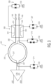
- Figure 3 is another circuit diagram showing a portion of circuitry of die 101.
- the primary winding of transformer 201 is implemented with a circular signal line 315 around a circular signal line 317 that is used to implement the second winding of transformer 201.
- signal lines 315 and 317 are implemented in a metal layer (not shown) in die 101 that is located above the semiconductor substrate (not shown) of die 101.
- a transformer may be implemented in a semiconductor die with other structures in other embodiments.
- signal lines 231 and 232 are implemented with a co-planer wave guide 300 that includes directional couplers 301 and 303.
- a directional coupler is a device used for sampling incident and/or reflected power of a signal.
- directional couplers 301 and 303 are each connected to an ESD clamp circuit 305 and 307, respectively, for discharging ESD current to VSSA rail 233 during an ESD event affecting terminal 105 or terminal 106 for protecting the directional couplers from damage.
- clamp circuits 305 and 307 are implemented with gated diodes in an anti-parallel configuration, but other types of clamp circuits may be utilized in other embodiments. Other embodiments may not include clamp circuits 305 and 307.
- clamp circuit 211 is implemented in a solder ball breakage detection circuit (not shown) of the semiconductor die 101, but may be implemented in other circuits of die 101 in other embodiments.
- Figure 4 is a circuit diagram of an LNA circuit 1clamp 11 according to another embodiment.
- the items in the embodiment of Figure 4 having the same reference numbers as the items in the embodiment of Figure 2 are similar.
- Circuit 211 of Figure 4 is different than circuit 211 of Figure 2 in that circuit 211 of Figure 4 has an additional VSSA external die terminal 401, an additional VSSA rail 407, an additional ESD GND rail 412, and an additional GND ESD terminal 416.
- Terminal 401 is configured to be biased at the same supply voltage as terminal 108
- terminal 416 is configured to be biased at the same supply voltage as terminal 109.
- Rail 407 is coupled to rail 412 with an ESD clamp circuit 404 that is similar to ESD clamp circuit 245.
- Center tap 207 is coupled to rail 407 with ESD clamp circuit 402, which in the embodiment shown in implemented with two diodes in an anti-parallel configuration.
- Center tap 208 is coupled to rail 407 with an ESD clamp circuit 403.
- clamp circuit 403 has a configuration similar to clamp circuit 215.
- An ESD clamp circuit (not shown) is coupled to VDD rail 234 and VSSA rail 407 for discharging ESD current between the two rails.
- the ESD clamp circuits 211, 215, 245, 305, 307, 402, 403, and 404 are implemented with diodes in an anti-parallel configuration.
- the Figures show the clamp circuits with diode paths of 1 or 2 diodes, other clamp circuits may include diode paths with a different number of diodes.
- these ESD clamp circuits may be implemented with other types of ESD clamp circuits such as clamp circuits with a transistor (e.g., FETs, bipolar transistors).
- FIG. 5 is a circuit diagram of an ESD clamp circuit according to another embodiment of the present invention.
- Clamp circuit 503 can used for clamp circuit 215 of Figure 2 and clamp circuit 403 of Figure 4 .
- Circuit 503 can also be used for circuits 211 and 402.
- clamp circuit 503 includes an NFET 505 with a source connected to rail 233 and its drain connected to center tap 208.
- the gate of NFET 505 is coupled to rail 233 through a resistor 507.
- resistor 507 is 500 ohms, but may be of other values in other embodiments, depending upon the desired threshold voltage of the clamp circuit.
- clamp circuit 503 is characterized as having a grounded gate NMOS configuration.
- the turn on threshold voltage of clamp circuit 503 is 3.1V.
- transformer 201 is utilized for ESD protection
- a transformer with a clamp circuit electrically coupling its secondary center tap to ground may be utilized in other types of circuits.
- such a transformer may be used to step down or step up a supply voltage.
- such a transformer may be used for ESD protection of non differential signal terminal inputs.
- the terminals of the secondary winding may be electrically coupled to external die terminals and the terminals of the primary winding may be coupled to internal circuitry.
- the primary center tap would be coupled to a supply rail with an ESD clamp circuit (e.g., similar to circuit 215) for ESD protection of the internal circuitry.
- ESD clamp circuit e.g., similar to circuit 215
- Such a transformer may be used by a semiconductor die in providing an output signal (e.g., to an antennae for transmission). Also, such a transformer may be used by a power supply controller for externally providing a step up or step down supply voltage.
- a source and drain are current terminals of a FET.
- a gate is a control terminal of a FET.
- a semiconductor die includes a transformer including a primary winding and a secondary winding.
- the primary winding includes a first terminal electrically coupled to a first external die terminal, a second terminal electrically coupled to a second external die terminal, and a first center tap.
- the secondary winding includes a third terminal, a fourth terminal, and a second center tap.
- the semiconductor die includes a first electrostatic discharge (ESD) clamp circuit including a fifth terminal electrically coupled to the first center tap and a sixth terminal electrically coupled to a supply rail. When made conductive in response to an ESD event affecting at least one of the first external die terminal and the second external die terminal, the first ESD clamp circuit discharges ESD current between the first center tap and the supply rail.
- ESD electrostatic discharge
- the semiconductor die includes a second ESD clamp circuit including a seventh terminal electrically coupled to the second center tap and an eighth terminal electrically coupled to the supply rail.
- the second ESD clamp circuit When made conductive in response to the ESD event affecting at least one of the first external die terminal and the second external die terminal, the second ESD clamp circuit discharges ESD current between the second center tap and the supply rail.
Landscapes
- Engineering & Computer Science (AREA)
- Power Engineering (AREA)
- Microelectronics & Electronic Packaging (AREA)
- Electronic Switches (AREA)
- Tone Control, Compression And Expansion, Limiting Amplitude (AREA)
- Amplifiers (AREA)
Claims (11)
- Halbleiterchip (101), der Folgendes umfasst:einen Transformator (201), der eine erste Wicklung undeine zweite Wicklung enthält, wobei:die erste Wicklung einen ersten Anschluss (203), der an einen ersten externen Chipanschluss (105) elektrisch gekoppelt ist, und einen zweiten Anschluss (204), der an einen zweiten externen Chipanschluss (106) elektrisch gekoppelt ist, enthält; unddie zweite Wicklung einen dritten Anschluss (205), einen vierten Anschluss (206) und einen Mittenabgriff (208) enthält, wobei:der dritte Anschluss und der vierte Anschluss an eine interne Schaltungsanordnung (217) des Halbleiterchips elektrisch gekoppelt sind;eine erste Klemmschaltung zur elektrostatischen Entladung (ESD-Klemmschaltung) (215), die einen fünften Anschluss, der an den Mittenabgriff (208) der zweiten Wicklung elektrisch gekoppelt ist, und einen sechsten Anschluss, der an eine Versorgungsschiene (233) elektrisch gekoppelt ist, enthält, wobei die ESD-Klemmschaltung dann, wenn sie während eines ESD-Ereignisses leitend gemacht wird, einen ESD-Strom zwischen dem Mittenabgriff und der Versorgungsschiene entlädt;wobei die erste Wicklung einen Mittenabgriff (207) enthält;der Halbleiterchip eine zweite ESD-Klemmschaltung (211) enthält, die einen siebten Anschluss, der an den Mittenabgriff (207) der ersten Wicklung elektrisch gekoppelt ist, und einen achten Anschluss, der an die Versorgungsschiene elektrisch gekoppelt ist, enthält, wobei die zweite ESD-Klemmschaltung dann, wenn sie während eines ESD-Ereignisses, das den ersten externen Chipanschluss und/oder den zweiten externen Chipanschluss beeinflusst, leitend gemacht wird, einen ESD-Strom zwischen dem Mittenabgriff der ersten Wicklung und der Versorgungsschiene entlädt.
- Halbleiterchip nach Anspruch 1, wobei die erste ESD-Klemmschaltung konfiguriert ist, einen ESD-Strom in Reaktion auf ein ESD-Ereignis, das den ersten externen Chipanschluss und/oder den zweiten externen Chipanschluss beeinflusst, zu entladen.
- Halbleiterchip nach Anspruch 1 oder 2, wobei der erste externe Chipanschluss und der zweite externe Chipanschluss konfiguriert sind, ein Differenzialeingangssignal zu empfangen.
- Halbleiterchip nach Anspruch 3, wobei das Differenzialeingangssignal bei einer Frequenz im Gigahertzbereich moduliert wird.
- Halbleiterchip nach einem der Ansprüche 1 bis 4, wobeider Halbleiterchip einen Verstärker (217) enthält;der dritte Anschluss an einen ersten Eingang des Verstärkers elektrisch gekoppelt ist und der vierte Anschluss an einen zweiten Eingang des Verstärkers elektrisch gekoppelt ist.
- Halbleiterchip nach Anspruch 5, der ferner eine Mischerschaltung (213) umfasst, die einen ersten Mischereingang, der an einen ersten Ausgang des Verstärkers elektrisch gekoppelt ist, und einen zweiten Mischereingang, der an einen zweiten Ausgang des Verstärkers elektrisch gekoppelt ist, enthält, wobei der erste Ausgang und der zweite Ausgang konfiguriert sind, ein Differenzialsignal bereitzustellen, das bei einer Frequenz im Gigahertzbereich moduliert ist, und die Mischerschaltung konfiguriert ist, ein zweites Differenzialsignal auf der Grundlage des Differenzialsignals zu erzeugen, das bei einer niedrigeren Frequenz als das Differenzialsignal moduliert ist.
- Halbleiterchip nach einem der Ansprüche 1 bis 6, wobei die erste ESD-Klemmschaltung einen Transistor (505) und einen Widerstand (507) enthält, der Transistor einen ersten Stromanschluss, der an den fünften Anschluss elektrisch gekoppelt ist, und einen zweiten Stromanschluss, der an den sechsten Anschluss elektrisch gekoppelt ist, enthält, der Transistor einen Steueranschluss enthält und der Widerstand in einen Strompfad zwischen dem Steueranschluss und der Versorgungsschiene gekoppelt ist.
- Halbleiterchip nach einem der Ansprüche 1 bis 7, wobei die erste Wicklung als eine Primärwicklung des Transformators charakterisiert ist und die zweite Wicklung als eine Sekundärwicklung des Transformators charakterisiert ist.
- Halbleiterchip nach einem der Ansprüche 1 bis 8, wobei die erste ESD-Klemmschaltung mindestens eine Diode (243) in einem ersten Diodenpfad und mindestens eine Diode (241) in einem zweiten Diodenpfad enthält und der erste Diodenpfad und der zweite Diodenpfad in einer antiparallelen Konfiguration sind.
- Halbleiterchip nach einem der Ansprüche 1 bis 9, wobei:der Mittenabgriff konfiguriert ist, eine Vorbelastungsspannung zu empfangen; unddie erste ESD-Klemmschaltung Folgendes enthält:eine erste Diode (243), die eine Kathode, die an den fünften Anschluss elektrisch gekoppelt ist, und eine Anode, die an den sechsten Anschluss elektrisch gekoppelt ist, enthält; undeine zweite Diode (241) und eine dritte Diode (242), die mit einer Kathode der zweiten Diode, die mit einer Anode der dritten Diode elektrisch verbunden ist, in Reihe geschaltet ist, wobei eine Anode der zweiten Diode an den fünften Anschluss elektrisch gekoppelt ist und eine Kathode der dritten Diode an die Versorgungsschiene elektrisch gekoppelt ist.
- Halbleiterchip nach einem der Ansprüche 1 bis 10, der ferner Folgendes umfasst:
einen komplanaren Hohlleiter (300), der Folgendes umfasst:eine erste Signalleitung (231) zum Bereitstellen einer Leiterbahn zwischen dem ersten externen Chipanschluss und dem ersten Anschluss der ersten Wicklung;eine zweite Signalleitung (232) zum Bereitstellen einer Leiterbahn zwischen dem zweiten externen Chipanschluss und dem zweiten Anschluss der ersten Wicklung;einen ersten Richtungskoppler (303);eine dritte ESD-Klemmschaltung (307), die an den ersten Richtungskoppler elektrisch gekoppelt ist, der einen siebten Anschluss, der an den ersten Richtungskoppler elektrisch gekoppelt ist, und einen achten Anschluss, der an eine Versorgungsschiene (233) elektrisch gekoppelt ist, enthält, wobei die dritte ESD-Klemmschaltung dann, wenn sie während eines ESD-Ereignisses leitend gemacht wird, einen ESD-Strom zwischen dem ersten Richtungskoppler und der Versorgungsschiene entlädt.
Applications Claiming Priority (1)
| Application Number | Priority Date | Filing Date | Title |
|---|---|---|---|
| US17/938,151 US12206237B2 (en) | 2022-10-05 | 2022-10-05 | Semiconductor die with transformer and ESD clamp circuit |
Publications (2)
| Publication Number | Publication Date |
|---|---|
| EP4350723A1 EP4350723A1 (de) | 2024-04-10 |
| EP4350723B1 true EP4350723B1 (de) | 2025-04-02 |
Family
ID=87863432
Family Applications (1)
| Application Number | Title | Priority Date | Filing Date |
|---|---|---|---|
| EP23194376.2A Active EP4350723B1 (de) | 2022-10-05 | 2023-08-30 | Halbleiterchip mit transformator und esd-klemmschaltung |
Country Status (3)
| Country | Link |
|---|---|
| US (1) | US12206237B2 (de) |
| EP (1) | EP4350723B1 (de) |
| CN (1) | CN117855196A (de) |
Family Cites Families (15)
| Publication number | Priority date | Publication date | Assignee | Title |
|---|---|---|---|---|
| US6784738B1 (en) | 2002-11-20 | 2004-08-31 | Marvell International Ltd. | Method and apparatus for gain control in a CMOS low noise amplifier |
| US7894173B2 (en) | 2008-09-16 | 2011-02-22 | Taiwan Semiconductor Manufacturing Company, Ltd. | Enhancing bandwidth of ESD network using transformers |
| US8213142B2 (en) | 2008-10-29 | 2012-07-03 | Qualcomm, Incorporated | Amplifier with improved ESD protection circuitry |
| IT1399907B1 (it) * | 2010-04-28 | 2013-05-09 | St Microelectronics Srl | Apparato di protezione contro scariche elettrostatiche per un circuito integrato e relativo circuito integrato. |
| US8942760B2 (en) | 2010-08-05 | 2015-01-27 | St-Ericsson Sa | Integrated bluetooth and wireless LAN transceivers having merged low noise and power amplifier |
| US8493705B2 (en) | 2010-12-30 | 2013-07-23 | Taiwan Semiconductor Manufacturing Co., Ltd. | Electrostatic discharge circuit for radio frequency transmitters |
| JP5828768B2 (ja) | 2012-01-05 | 2015-12-09 | パナソニック株式会社 | 保護回路 |
| US8817437B2 (en) * | 2013-01-03 | 2014-08-26 | Amazing Microelectronics Corp. | High voltage open-drain electrostatic discharge (ESD) protection device |
| US9548293B2 (en) * | 2014-02-14 | 2017-01-17 | Infineon Technologies Ag | III-nitride based ESD protection device |
| US9847291B2 (en) * | 2014-04-02 | 2017-12-19 | Marvell World Trade Ltd. | Circuits incorporating integrated passive devices having inductances in 3D configurations and stacked with corresponding dies |
| US9806521B2 (en) | 2014-10-29 | 2017-10-31 | Silicon Laboratories Inc. | Electrostatic discharge protection for a transformer balun |
| TWI561017B (en) | 2015-01-22 | 2016-12-01 | Airoha Tech Corp | Wireless transceiver chip |
| US9735145B2 (en) | 2015-02-18 | 2017-08-15 | Silicon Laboratories Inc. | Electrostatic discharge protection for a balun |
| JP2016171163A (ja) | 2015-03-12 | 2016-09-23 | ルネサスエレクトロニクス株式会社 | 半導体集積回路、通信モジュール、及びスマートメータ |
| US11380993B2 (en) | 2019-12-19 | 2022-07-05 | Globalfoundries U.S. Inc. | Transceiver front-end with receiver branch matching network including integrated electrostatic discharge protection |
-
2022
- 2022-10-05 US US17/938,151 patent/US12206237B2/en active Active
-
2023
- 2023-08-30 EP EP23194376.2A patent/EP4350723B1/de active Active
- 2023-09-27 CN CN202311263329.2A patent/CN117855196A/zh active Pending
Also Published As
| Publication number | Publication date |
|---|---|
| EP4350723A1 (de) | 2024-04-10 |
| US20240120734A1 (en) | 2024-04-11 |
| CN117855196A (zh) | 2024-04-09 |
| US12206237B2 (en) | 2025-01-21 |
Similar Documents
| Publication | Publication Date | Title |
|---|---|---|
| JP6285483B2 (ja) | ダイオード、それを使用する回路、および製造方法 | |
| US8531805B2 (en) | Gated diode having at least one lightly-doped drain (LDD) implant blocked and circuits and methods employing same | |
| US9831666B2 (en) | Apparatus and methods for electrostatic discharge protection of radio frequency interfaces | |
| US7265433B2 (en) | On-pad broadband matching network | |
| US20140273825A1 (en) | Semiconductor Chip Configuration with a Coupler | |
| US6624999B1 (en) | Electrostatic discharge protection using inductors | |
| CN113114297B (zh) | 具有包括集成静电放电保护的接收器支路匹配网络的收发器前端 | |
| US12356686B2 (en) | Devices related to switch body connections to achieve soft breakdown | |
| US12278486B2 (en) | Electrostatic discharge protection for RF pins | |
| US8643427B2 (en) | Switching device | |
| US11621670B1 (en) | Capacitively-coupled stacked class-d oscillators for galvanic isolation | |
| EP4350723B1 (de) | Halbleiterchip mit transformator und esd-klemmschaltung | |
| CN100508192C (zh) | 输出/入元件与控制具数个输出/入元件的集成电路的方法 | |
| US11462493B2 (en) | Method and system for improved noise isolation in an electrostatic discharge protection scheme | |
| US6031270A (en) | Methods of protecting a semiconductor device | |
| US11901863B2 (en) | Capacitively-coupled stacked class-D oscillators for galvanic isolation | |
| US12477836B2 (en) | Low capacitance silicon controlled rectifier topology for overvoltage protection | |
| US7388734B2 (en) | Integrated circiut arrangement | |
| JP2002118123A (ja) | 化合物半導体スイッチ回路装置 | |
| JP2002231897A (ja) | 化合物半導体スイッチ回路装置 |
Legal Events
| Date | Code | Title | Description |
|---|---|---|---|
| PUAI | Public reference made under article 153(3) epc to a published international application that has entered the european phase |
Free format text: ORIGINAL CODE: 0009012 |
|
| STAA | Information on the status of an ep patent application or granted ep patent |
Free format text: STATUS: THE APPLICATION HAS BEEN PUBLISHED |
|
| AK | Designated contracting states |
Kind code of ref document: A1 Designated state(s): AL AT BE BG CH CY CZ DE DK EE ES FI FR GB GR HR HU IE IS IT LI LT LU LV MC ME MK MT NL NO PL PT RO RS SE SI SK SM TR |
|
| STAA | Information on the status of an ep patent application or granted ep patent |
Free format text: STATUS: REQUEST FOR EXAMINATION WAS MADE |
|
| 17P | Request for examination filed |
Effective date: 20241010 |
|
| RBV | Designated contracting states (corrected) |
Designated state(s): AL AT BE BG CH CY CZ DE DK EE ES FI FR GB GR HR HU IE IS IT LI LT LU LV MC ME MK MT NL NO PL PT RO RS SE SI SK SM TR |
|
| GRAP | Despatch of communication of intention to grant a patent |
Free format text: ORIGINAL CODE: EPIDOSNIGR1 |
|
| STAA | Information on the status of an ep patent application or granted ep patent |
Free format text: STATUS: GRANT OF PATENT IS INTENDED |
|
| INTG | Intention to grant announced |
Effective date: 20241126 |
|
| GRAS | Grant fee paid |
Free format text: ORIGINAL CODE: EPIDOSNIGR3 |
|
| GRAA | (expected) grant |
Free format text: ORIGINAL CODE: 0009210 |
|
| STAA | Information on the status of an ep patent application or granted ep patent |
Free format text: STATUS: THE PATENT HAS BEEN GRANTED |
|
| AK | Designated contracting states |
Kind code of ref document: B1 Designated state(s): AL AT BE BG CH CY CZ DE DK EE ES FI FR GB GR HR HU IE IS IT LI LT LU LV MC ME MK MT NL NO PL PT RO RS SE SI SK SM TR |
|
| REG | Reference to a national code |
Ref country code: GB Ref legal event code: FG4D |
|
| REG | Reference to a national code |
Ref country code: CH Ref legal event code: EP |
|
| REG | Reference to a national code |
Ref country code: IE Ref legal event code: FG4D |
|
| REG | Reference to a national code |
Ref country code: DE Ref legal event code: R096 Ref document number: 602023002708 Country of ref document: DE |
|
| REG | Reference to a national code |
Ref country code: NL Ref legal event code: MP Effective date: 20250402 |
|
| PG25 | Lapsed in a contracting state [announced via postgrant information from national office to epo] |
Ref country code: NL Free format text: LAPSE BECAUSE OF FAILURE TO SUBMIT A TRANSLATION OF THE DESCRIPTION OR TO PAY THE FEE WITHIN THE PRESCRIBED TIME-LIMIT Effective date: 20250402 |
|
| REG | Reference to a national code |
Ref country code: AT Ref legal event code: MK05 Ref document number: 1782150 Country of ref document: AT Kind code of ref document: T Effective date: 20250402 |
|
| PG25 | Lapsed in a contracting state [announced via postgrant information from national office to epo] |
Ref country code: FI Free format text: LAPSE BECAUSE OF FAILURE TO SUBMIT A TRANSLATION OF THE DESCRIPTION OR TO PAY THE FEE WITHIN THE PRESCRIBED TIME-LIMIT Effective date: 20250402 Ref country code: PT Free format text: LAPSE BECAUSE OF FAILURE TO SUBMIT A TRANSLATION OF THE DESCRIPTION OR TO PAY THE FEE WITHIN THE PRESCRIBED TIME-LIMIT Effective date: 20250804 Ref country code: ES Free format text: LAPSE BECAUSE OF FAILURE TO SUBMIT A TRANSLATION OF THE DESCRIPTION OR TO PAY THE FEE WITHIN THE PRESCRIBED TIME-LIMIT Effective date: 20250402 |
|
| PGFP | Annual fee paid to national office [announced via postgrant information from national office to epo] |
Ref country code: DE Payment date: 20250724 Year of fee payment: 3 |
|
| REG | Reference to a national code |
Ref country code: LT Ref legal event code: MG9D |
|
| PG25 | Lapsed in a contracting state [announced via postgrant information from national office to epo] |
Ref country code: NO Free format text: LAPSE BECAUSE OF FAILURE TO SUBMIT A TRANSLATION OF THE DESCRIPTION OR TO PAY THE FEE WITHIN THE PRESCRIBED TIME-LIMIT Effective date: 20250702 Ref country code: GR Free format text: LAPSE BECAUSE OF FAILURE TO SUBMIT A TRANSLATION OF THE DESCRIPTION OR TO PAY THE FEE WITHIN THE PRESCRIBED TIME-LIMIT Effective date: 20250703 |
|
| PG25 | Lapsed in a contracting state [announced via postgrant information from national office to epo] |
Ref country code: PL Free format text: LAPSE BECAUSE OF FAILURE TO SUBMIT A TRANSLATION OF THE DESCRIPTION OR TO PAY THE FEE WITHIN THE PRESCRIBED TIME-LIMIT Effective date: 20250402 |
|
| PG25 | Lapsed in a contracting state [announced via postgrant information from national office to epo] |
Ref country code: BG Free format text: LAPSE BECAUSE OF FAILURE TO SUBMIT A TRANSLATION OF THE DESCRIPTION OR TO PAY THE FEE WITHIN THE PRESCRIBED TIME-LIMIT Effective date: 20250402 |
|
| PG25 | Lapsed in a contracting state [announced via postgrant information from national office to epo] |
Ref country code: HR Free format text: LAPSE BECAUSE OF FAILURE TO SUBMIT A TRANSLATION OF THE DESCRIPTION OR TO PAY THE FEE WITHIN THE PRESCRIBED TIME-LIMIT Effective date: 20250402 |
|
| PG25 | Lapsed in a contracting state [announced via postgrant information from national office to epo] |
Ref country code: AT Free format text: LAPSE BECAUSE OF FAILURE TO SUBMIT A TRANSLATION OF THE DESCRIPTION OR TO PAY THE FEE WITHIN THE PRESCRIBED TIME-LIMIT Effective date: 20250402 |
|
| PGFP | Annual fee paid to national office [announced via postgrant information from national office to epo] |
Ref country code: FR Payment date: 20250723 Year of fee payment: 3 |
|
| PG25 | Lapsed in a contracting state [announced via postgrant information from national office to epo] |
Ref country code: RS Free format text: LAPSE BECAUSE OF FAILURE TO SUBMIT A TRANSLATION OF THE DESCRIPTION OR TO PAY THE FEE WITHIN THE PRESCRIBED TIME-LIMIT Effective date: 20250702 |
|
| PG25 | Lapsed in a contracting state [announced via postgrant information from national office to epo] |
Ref country code: IS Free format text: LAPSE BECAUSE OF FAILURE TO SUBMIT A TRANSLATION OF THE DESCRIPTION OR TO PAY THE FEE WITHIN THE PRESCRIBED TIME-LIMIT Effective date: 20250802 |
|
| PG25 | Lapsed in a contracting state [announced via postgrant information from national office to epo] |
Ref country code: LV Free format text: LAPSE BECAUSE OF FAILURE TO SUBMIT A TRANSLATION OF THE DESCRIPTION OR TO PAY THE FEE WITHIN THE PRESCRIBED TIME-LIMIT Effective date: 20250402 |
|
| REG | Reference to a national code |
Ref country code: DE Ref legal event code: R097 Ref document number: 602023002708 Country of ref document: DE |
|
| PG25 | Lapsed in a contracting state [announced via postgrant information from national office to epo] |
Ref country code: DK Free format text: LAPSE BECAUSE OF FAILURE TO SUBMIT A TRANSLATION OF THE DESCRIPTION OR TO PAY THE FEE WITHIN THE PRESCRIBED TIME-LIMIT Effective date: 20250402 Ref country code: SM Free format text: LAPSE BECAUSE OF FAILURE TO SUBMIT A TRANSLATION OF THE DESCRIPTION OR TO PAY THE FEE WITHIN THE PRESCRIBED TIME-LIMIT Effective date: 20250402 |
|
| PG25 | Lapsed in a contracting state [announced via postgrant information from national office to epo] |
Ref country code: CZ Free format text: LAPSE BECAUSE OF FAILURE TO SUBMIT A TRANSLATION OF THE DESCRIPTION OR TO PAY THE FEE WITHIN THE PRESCRIBED TIME-LIMIT Effective date: 20250402 |
|
| PG25 | Lapsed in a contracting state [announced via postgrant information from national office to epo] |
Ref country code: EE Free format text: LAPSE BECAUSE OF FAILURE TO SUBMIT A TRANSLATION OF THE DESCRIPTION OR TO PAY THE FEE WITHIN THE PRESCRIBED TIME-LIMIT Effective date: 20250402 |
|
| PG25 | Lapsed in a contracting state [announced via postgrant information from national office to epo] |
Ref country code: SK Free format text: LAPSE BECAUSE OF FAILURE TO SUBMIT A TRANSLATION OF THE DESCRIPTION OR TO PAY THE FEE WITHIN THE PRESCRIBED TIME-LIMIT Effective date: 20250402 |
|
| PG25 | Lapsed in a contracting state [announced via postgrant information from national office to epo] |
Ref country code: IT Free format text: LAPSE BECAUSE OF FAILURE TO SUBMIT A TRANSLATION OF THE DESCRIPTION OR TO PAY THE FEE WITHIN THE PRESCRIBED TIME-LIMIT Effective date: 20250402 |
|
| PLBE | No opposition filed within time limit |
Free format text: ORIGINAL CODE: 0009261 |
|
| STAA | Information on the status of an ep patent application or granted ep patent |
Free format text: STATUS: NO OPPOSITION FILED WITHIN TIME LIMIT |
|
| REG | Reference to a national code |
Ref country code: CH Ref legal event code: L10 Free format text: ST27 STATUS EVENT CODE: U-0-0-L10-L00 (AS PROVIDED BY THE NATIONAL OFFICE) Effective date: 20260211 |
|
| PG25 | Lapsed in a contracting state [announced via postgrant information from national office to epo] |
Ref country code: RO Free format text: LAPSE BECAUSE OF FAILURE TO SUBMIT A TRANSLATION OF THE DESCRIPTION OR TO PAY THE FEE WITHIN THE PRESCRIBED TIME-LIMIT Effective date: 20250402 |
|
| 26N | No opposition filed |
Effective date: 20260105 |
|
| PG25 | Lapsed in a contracting state [announced via postgrant information from national office to epo] |
Ref country code: MC Free format text: LAPSE BECAUSE OF FAILURE TO SUBMIT A TRANSLATION OF THE DESCRIPTION OR TO PAY THE FEE WITHIN THE PRESCRIBED TIME-LIMIT Effective date: 20250402 |
|
| PG25 | Lapsed in a contracting state [announced via postgrant information from national office to epo] |
Ref country code: LU Free format text: LAPSE BECAUSE OF NON-PAYMENT OF DUE FEES Effective date: 20250830 |