EP4350780A1 - Photoelektrisches umwandlungselement, solarzellenmodul und paddel - Google Patents
Photoelektrisches umwandlungselement, solarzellenmodul und paddel Download PDFInfo
- Publication number
- EP4350780A1 EP4350780A1 EP22816083.4A EP22816083A EP4350780A1 EP 4350780 A1 EP4350780 A1 EP 4350780A1 EP 22816083 A EP22816083 A EP 22816083A EP 4350780 A1 EP4350780 A1 EP 4350780A1
- Authority
- EP
- European Patent Office
- Prior art keywords
- photoelectric conversion
- layer
- conversion element
- electrode layer
- collecting electrode
- Prior art date
- Legal status (The legal status is an assumption and is not a legal conclusion. Google has not performed a legal analysis and makes no representation as to the accuracy of the status listed.)
- Pending
Links
Images


Classifications
-
- H—ELECTRICITY
- H10—SEMICONDUCTOR DEVICES; ELECTRIC SOLID-STATE DEVICES NOT OTHERWISE PROVIDED FOR
- H10F—INORGANIC SEMICONDUCTOR DEVICES SENSITIVE TO INFRARED RADIATION, LIGHT, ELECTROMAGNETIC RADIATION OF SHORTER WAVELENGTH OR CORPUSCULAR RADIATION
- H10F10/00—Individual photovoltaic cells, e.g. solar cells
- H10F10/10—Individual photovoltaic cells, e.g. solar cells having potential barriers
- H10F10/16—Photovoltaic cells having only PN heterojunction potential barriers
- H10F10/167—Photovoltaic cells having only PN heterojunction potential barriers comprising Group I-III-VI materials, e.g. CdS/CuInSe2 [CIS] heterojunction photovoltaic cells
-
- B—PERFORMING OPERATIONS; TRANSPORTING
- B64—AIRCRAFT; AVIATION; COSMONAUTICS
- B64G—COSMONAUTICS; VEHICLES OR EQUIPMENT THEREFOR
- B64G1/00—Cosmonautic vehicles
- B64G1/22—Parts of, or equipment specially adapted for fitting in or to, cosmonautic vehicles
- B64G1/42—Arrangements or adaptations of power supply systems
- B64G1/44—Arrangements or adaptations of power supply systems using radiation, e.g. deployable solar arrays
- B64G1/443—Photovoltaic cell arrays
-
- H—ELECTRICITY
- H10—SEMICONDUCTOR DEVICES; ELECTRIC SOLID-STATE DEVICES NOT OTHERWISE PROVIDED FOR
- H10F—INORGANIC SEMICONDUCTOR DEVICES SENSITIVE TO INFRARED RADIATION, LIGHT, ELECTROMAGNETIC RADIATION OF SHORTER WAVELENGTH OR CORPUSCULAR RADIATION
- H10F19/00—Integrated devices, or assemblies of multiple devices, comprising at least one photovoltaic cell covered by group H10F10/00, e.g. photovoltaic modules
- H10F19/90—Structures for connecting between photovoltaic cells, e.g. interconnections or insulating spacers
- H10F19/902—Structures for connecting between photovoltaic cells, e.g. interconnections or insulating spacers for series or parallel connection of photovoltaic cells
-
- H—ELECTRICITY
- H10—SEMICONDUCTOR DEVICES; ELECTRIC SOLID-STATE DEVICES NOT OTHERWISE PROVIDED FOR
- H10F—INORGANIC SEMICONDUCTOR DEVICES SENSITIVE TO INFRARED RADIATION, LIGHT, ELECTROMAGNETIC RADIATION OF SHORTER WAVELENGTH OR CORPUSCULAR RADIATION
- H10F77/00—Constructional details of devices covered by this subclass
- H10F77/10—Semiconductor bodies
- H10F77/16—Material structures, e.g. crystalline structures, film structures or crystal plane orientations
- H10F77/162—Non-monocrystalline materials, e.g. semiconductor particles embedded in insulating materials
- H10F77/166—Amorphous semiconductors
- H10F77/1662—Amorphous semiconductors including only Group IV materials
-
- H—ELECTRICITY
- H10—SEMICONDUCTOR DEVICES; ELECTRIC SOLID-STATE DEVICES NOT OTHERWISE PROVIDED FOR
- H10F—INORGANIC SEMICONDUCTOR DEVICES SENSITIVE TO INFRARED RADIATION, LIGHT, ELECTROMAGNETIC RADIATION OF SHORTER WAVELENGTH OR CORPUSCULAR RADIATION
- H10F77/00—Constructional details of devices covered by this subclass
- H10F77/20—Electrodes
- H10F77/206—Electrodes for devices having potential barriers
- H10F77/211—Electrodes for devices having potential barriers for photovoltaic cells
- H10F77/215—Geometries of grid contacts
-
- H—ELECTRICITY
- H10—SEMICONDUCTOR DEVICES; ELECTRIC SOLID-STATE DEVICES NOT OTHERWISE PROVIDED FOR
- H10F—INORGANIC SEMICONDUCTOR DEVICES SENSITIVE TO INFRARED RADIATION, LIGHT, ELECTROMAGNETIC RADIATION OF SHORTER WAVELENGTH OR CORPUSCULAR RADIATION
- H10F77/00—Constructional details of devices covered by this subclass
- H10F77/20—Electrodes
- H10F77/206—Electrodes for devices having potential barriers
- H10F77/211—Electrodes for devices having potential barriers for photovoltaic cells
- H10F77/219—Arrangements for electrodes of back-contact photovoltaic cells
-
- Y—GENERAL TAGGING OF NEW TECHNOLOGICAL DEVELOPMENTS; GENERAL TAGGING OF CROSS-SECTIONAL TECHNOLOGIES SPANNING OVER SEVERAL SECTIONS OF THE IPC; TECHNICAL SUBJECTS COVERED BY FORMER USPC CROSS-REFERENCE ART COLLECTIONS [XRACs] AND DIGESTS
- Y02—TECHNOLOGIES OR APPLICATIONS FOR MITIGATION OR ADAPTATION AGAINST CLIMATE CHANGE
- Y02E—REDUCTION OF GREENHOUSE GAS [GHG] EMISSIONS, RELATED TO ENERGY GENERATION, TRANSMISSION OR DISTRIBUTION
- Y02E10/00—Energy generation through renewable energy sources
- Y02E10/50—Photovoltaic [PV] energy
- Y02E10/541—CuInSe2 material PV cells
Definitions
- the present invention relates to a photoelectric conversion element, a solar cell module, and a paddle.
- Patent Literature 1 A photoelectric conversion element that converts light energy into electric energy is known (Patent Literature 1).
- the photoelectric conversion element described in Patent Literature 1 includes a substrate made of an insulating material, a back electrode layer formed on the substrate, a power generation layer formed on the back electrode layer, a transparent electrode layer formed on the power generation layer, and a collecting electrode formed on the transparent electrode layer, the collecting electrode being made of metal.
- the collecting electrode includes a plurality of finger portions that collect electrons from the transparent electrode layer, and a bus bar portion that further collect electrons collected by the finger portions.
- the finger portion is formed in an elongated line-like shape extending from the bus bar portion.
- Patent Literature 1 JP 2009-302274 A
- the inventors of the present application found a problem that peeling may occur in a layer constituting a photoelectric conversion element at a position of a collecting electrode due to a temperature change in the photoelectric conversion element. When such peeling occurs, the photoelectric conversion efficiency of the photoelectric conversion element may decrease, or the photoelectric conversion function may be lost.
- a photoelectric conversion element comprises: a photoelectric conversion layer; an electrode layer adjacent to the photoelectric conversion layer; and a collecting electrode adjacent to the electrode layer.
- the collecting electrode has a line-like first portion. Where L is a length of the first portion, W is a width of the first portion, and D is a thickness of the first portion, "D ⁇ L/W" is less than 2.5 ⁇ 10 3 pm.
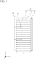
- Fig. 1 is a schematic plan view of a photoelectric conversion element according to a first embodiment.
- Fig. 2 is an enlarged view in the vicinity of a region 2A in Fig. 1 .
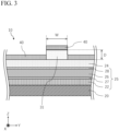
- Fig. 3 is a schematic cross-sectional view of the photoelectric conversion element taken along line 3A-3A in Fig. 2 . Note that in Fig. 2 , a reflection suppressing film 40 on a collecting electrode 30, which will be described later, is not illustrated for convenience of description.
- a photoelectric conversion element 10 may be a photoelectric conversion element of a thin film type.
- the photoelectric conversion element 10 is a solar cell element that converts light energy into electrical energy.
- a substrate 20 may be constructed by, for example, glass, ceramics, resin, metal, or the like.
- the photoelectric conversion element 10 may include at least a first electrode layer 22, a second electrode layer 24, and a laminated body 25 provided between the first electrode layer 22 and the second electrode layer 24.
- the laminated body 25 may include a photoelectric conversion layer 26 that contributes to mutual conversion of light energy and electric energy.
- the photoelectric conversion layer 26 may be referred to as a light absorption layer.
- the first electrode layer 22 and the second electrode layer 24 are adjacent to the photoelectric conversion layer 26.
- adjacent shall mean not only that both layers are in direct contact but also that both layers are in proximity via another layer.
- the first electrode layer 22 is provided between the photoelectric conversion layer 26 and the substrate 20.
- the second electrode layer 24 is located on a side opposite to the substrate 20 with respect to the photoelectric conversion layer 26. Therefore, the first electrode layer 22 is located on a side opposite to the second electrode layer 24 with respect to the photoelectric conversion layer 26.
- the second electrode layer 24 may be constituted by a transparent electrode layer.
- the second electrode layer 24 is constituted by a transparent electrode layer, light incident on the photoelectric conversion layer 26 or emitted from the photoelectric conversion layer 26 passes through the second electrode layer 24.
- the first electrode layer 22 may be constituted by an opaque electrode layer or may be constituted by a transparent electrode layer.
- the first electrode layer 22 may be formed of, for example, a metal such as molybdenum, titanium, or chromium.
- the second electrode layer 24 may be formed of an n-type semiconductor, more specifically, a material having n-type conductivity and relatively low resistance.
- the second electrode layer 24 may include, for example, a metal oxide to which a group III element (B, Al, Ga, or In) is added as a dopant. Examples of the metal oxide include ZnO and SnO 2 .
- the second electrode layer 24 can be selected, as an example of the above-described material or another material, from In 2 O 3 (indium oxide), ITO (indium tin oxide), ITiO (indium titanium oxide), IZO (indium zinc oxide), ZTO (zinc tin oxide), FTO (fluorine doped tin oxide), GZO (gallium doped zinc oxide), BZO (boron doped zinc oxide), AZO (aluminum doped zinc oxide), hydrogen doped indium oxide, and the like.
- the second electrode layer 24 can function as both an n-type semiconductor and a transparent electrode layer.
- the photoelectric conversion layer 26 may include, for example, a p-type semiconductor.
- the photoelectric conversion layer 26 may function as, for example, a p-type compound semiconductor layer of polycrystalline or microcrystalline.
- the photoelectric conversion layer 26 may have a CIS-based light absorption layer.
- the photoelectric conversion layer 26 is formed of a group I-III-VI 2 compound semiconductor having a chalcopyrite structure containing a group I element (Cu, Ag, Au, etc.), a group III element (Al, Ga, In, etc.), and a group VI element (O, S, Se, Te, etc.).
- the photoelectric conversion layer 26 is not limited to those described above, and may be constructed by any material that causes photoelectric conversion.
- the photoelectric conversion layer 26 may contain an alkali metal such as Li, Na, K, Rb, or Cs.
- the laminated structure of the photoelectric conversion element 10 is not limited to the above aspect, and may have any of various aspects.
- the photoelectric conversion element 10 may have a configuration in which both the n-type semiconductor and the p-type semiconductor are sandwiched between the first electrode layer and the second electrode layer.
- the second electrode layer need not be constituted by an n-type semiconductor.
- the photoelectric conversion element 10 is not limited to the p-n junction type structure, and may have a p-i-n junction type structure including an intrinsic semiconductor layer (i-type semiconductor) between an n-type semiconductor and a p-type semiconductor.
- the laminated body 25 may have a second buffer layer 28 between the photoelectric conversion layer 26 and the second electrode layer 24 as necessary.
- the second buffer layer 28 may be a semiconductor material having the same conductivity type as the second electrode layer 24, or may be a semiconductor material having a different conductivity type.
- the second buffer layer 28 may be constructed by a material having higher electric resistance than that of the second electrode layer 24.
- the second buffer layer 28 may be, for example, a Zn-based buffer layer, a Cd-based buffer layer, or an In-based buffer layer.
- the Zn-based buffer layer may be, for example, ZnS, ZnO, Zn(OH) 2 , ZnMgO, or a mixture, a mixed crystal, or a laminated body thereof.
- the Cd-based buffer layer may be, for example, CdS, CdO, Cd(OH) 2 , or a mixture, a mixed crystal, or a laminated body thereof.
- the In-based buffer layer may be, for example, In 2 S 3 , In 2 O 3 , In(OH) 3 , or a mixture, a mixed crystal, or a laminated body thereof.
- the laminated body 25 may have a first buffer layer 27 between the photoelectric conversion layer 26 and the first electrode layer 22 as necessary.
- the first buffer layer 27 may be a semiconductor material having the same conductivity type as the first electrode layer 22, or may be a semiconductor material having a different conductivity type.
- the first buffer layer 27 may be constructed by a material having higher electric resistance than that of the first electrode layer 22.
- the first buffer layer 27 is not particularly limited, but may be, for example, a layer containing a chalcogenide compound of a transition metal element having a layered structure.
- the first buffer layer 27 may be constructed by a compound containing a transition metal material such as Mo, W, Ti, V, Cr, Nb, or Ta and a chalcogen element such as O, S, or Se.
- the first buffer layer 27 may be, for example, a Mo(Se,S) 2 layer, a MoSe 2 layer, a MoS 2 layer, a Cr x TaS 2 layer, or the like.
- the layer having the above-described layered structure is a layer having cleavability.
- the layer having cleavability may be a layer having a hexagonal crystal structure.
- the photoelectric conversion element 10 includes a collecting electrode 30 adjacent to the second electrode layer 24.
- the collecting electrode 30 collects charge carriers from the second electrode layer 24, and is formed of a conductive material.
- the collecting electrode 30 may be in direct contact with the second electrode layer 24.
- the collecting electrode 30 may have a first portion 31 that has substantially line-like shape and a second portion 32 connected to the first portion 31.
- the collecting electrode 30 (the first portion 31 and the second portion 32) may be formed by a material having higher conductivity than that of the material constituting the second electrode layer 24.
- the collecting electrode 30 (the first portion 31 and the second portion 32) may include, for example, one or a plurality of materials selected from Ni, Mo, Ti, Cr, Al, Ag, Cu, Au, and the like.
- the collecting electrode 30 may include an alloy or a laminated body formed by a combination of the above-described materials.
- the substantially line-like first portion 31 extends straight along one direction (X direction in the drawing).
- the first portion 31 may extend in a wavy line shape or a zigzag polygonal line shape.
- line-like is defined by a concept including not only a straight line but also an elongated curved line such as a wavy line or a polygonal line.
- a plurality of the first portions 31 of the collecting electrode 30 may be provided side by side in the first direction (Y direction in the drawing).
- the plurality of first portions 31 may be connected to the same second portion 32.
- the first portion 31 of the collecting electrode 30 may have, at an end opposite to the second portion 32, one or a plurality of protrusions 31a protruding in a direction (Y direction in the drawing) intersecting a direction in which the line-like first portion 31 extends. Since a region of an end (free end) of the first portion 31 is expanded by the protrusion 31a, thermal stress generated in the region of the end (free end) of the first portion 31 can be dispersed. In the illustrated form, the plurality of protrusions 31a are provided in the region of the end (free end) of the first portion 31.
- the second portion 32 of the collecting electrode 30 may extend in a first direction (Y direction in the drawing).
- the second portion 32 may be connected to the first portion 31 at an end of the first portion 31.
- the plurality of first portions 31 may extend from the second portion 32 along the second direction.
- the second direction is a direction (X direction in the drawing) intersecting the above-described first direction.
- the second portion 32 of the collecting electrode 30 may extend from substantially the vicinity of one end to the vicinity of the other end of the photoelectric conversion element 10 in the first direction (Y direction in the drawing).
- the second portion 32 of the collecting electrode 30 may be larger than each of the first portions 31.
- the width of the second portion 32 in the X direction in the drawing may be larger than the width of the first portion 31 in the Y direction in the drawing.
- the photoelectric conversion element 10 may include a reflection suppressing film 40 that suppresses reflection of light.
- the reflection suppressing film 40 may be provided on, for example, both the collecting electrode 30 and the second electrode layer 24 on which the collecting electrode 30 is not formed.
- the inventor of the present application found that the photoelectric conversion element is peeled off or destroyed by a temperature cycle test at the free end of the first portion 31 of the collecting electrode 30 according to a design of length, width, and thickness of the first portion 31 of the collecting electrode 30. From such a viewpoint, the inventor has found a preferable condition regarding the length, the width, and the thickness of the first portion 31 of the collecting electrode 30. Hereinafter, the condition will be described.
- the length of the first portion 31 along the direction in which the first portion 31 extends is referred to as "L".
- the length L of the first portion 31 is defined by a distance from a connection portion of the first portion 31 with the second portion 32 to an end of the first portion 31 opposite to the second portion 32.
- the width of the first portion 31 in a direction (Y direction in the drawing) intersecting the direction in which the first portion 31 extends is referred to as "W".
- W may be a width of a portion not including the protrusion 31a described above.
- D the thickness of the first portion 31 is denoted by "D”.
- the first portion 31 of the collecting electrode 30 thermally expands/contracts due to a temperature change.
- One end of the first portion 31 is fixed to a relatively large second portion 32 (fixed end). Therefore, the other end portion (free end) of the first portion 31 thermally expands and contracts on a relatively free basis. That is, it is considered that an influence of thermal stress generated in the first portion 31 of the collecting electrode 30 is concentrated on the free end of the first portion 31.
- the concentration of the thermal stress also affects the width W of the first portion 31. That is, when the width W of the first portion 31 is small, an area of the first portion 31 is small, so that the thermal stress concentrates on a local region accordingly. Therefore, a degree of concentration (density) of the thermal stress in the vicinity of the free end of the first portion 31 is substantially proportional to a ratio of the length L and the width W of the first portion 31 (hereinafter referred to as "aspect ratio L/W").
- thermal stress generated in a thin film is proportional to a film thickness. Therefore, the thermal stress generated in the first portion 31 of the collecting electrode 30 is also proportional to a thickness D. Therefore, it can be seen that the degree of concentration (density) of the thermal stress in the vicinity of the free end of the first portion 31 is generally expressed by an index of "D ⁇ L/W".
- "D ⁇ L/W” is less than 2.5 ⁇ 10 3 um, and may be, for example, 2.4 ⁇ 10 3 um or less.
- "D ⁇ L/W” is 2.2 ⁇ 10 3 um or less. More preferably, “D ⁇ L/W” is 1.8 ⁇ 10 3 um or less. Furthermore preferably, “D ⁇ L/W” is 1.4 ⁇ 10 3 um or less.
- a photoelectric conversion element having high resistance to a temperature change can be provided. Note that a lower limit value of "D ⁇ L/W” is not particularly limited, and it is sufficient that "D ⁇ L/W" is, for example, larger than 0.
- L/W may be, for example, 6.25 ⁇ 10 2 or less.
- “L/W” is 5.6 ⁇ 10 2 or less. More preferably, “L/W” is 5.0 ⁇ 10 2 or less. Furthermore preferably, “L/W” is 4.4 ⁇ 10 2 or less. Even more preferably, “L/W” is 3.6 ⁇ 10 2 or less.
- a value of "L/W” is set so as not to exceed the upper limit value of "D ⁇ L/W” described above. Note that “L/W” is not particularly limited, but may be, for example, larger than 1.0.
- the thickness D of the first portion 31 may be, for example, 12 um or less.
- the thickness D of the first portion 31 is 8 um or less. More preferably, the thickness D of the first portion 31 is 6 um or less. Further preferably, the thickness D of the first portion 31 is 4 um or less.
- the thickness D of the first portion 31 is set so as not to exceed the upper limit value of "D ⁇ L/W" described above.
- the lower limit value of the thickness D of the first portion 31 is not particularly limited, and it is sufficient that the thickness D is, for example, larger than 0 ⁇ m.
- a photoelectric conversion layer 26 was a CIS-based light absorption layer
- a first electrode layer 22 was formed of molybdenum
- a first buffer layer 27 was a Mo (Se, S) 2 layer
- a second electrode layer 24 was a transparent electrode layer.
- the collecting electrode 30 (the first portion 31 and the second portion 32) was formed of a laminated body of nickel and silver.
- the thickness of nickel constituting the collecting electrode 30 was 10 nm.
- the total thickness of nickel and silver constituting the collecting electrode 30, that is, the thickness D described above was changed for each sample (condition) as shown in Table 1 below.
- a photoelectric conversion element including the collecting electrode 30 having the first portions 31 of different lengths L and widths W from each other was prepared, and a temperature cycle test was performed based on a difference in the length L, the width W, and the thickness D of the first portion 31.
- the length L of the first portion 31 is defined by a distance from a connection portion of the first portion 31 with the second portion 32 to an end of the first portion 31 opposite to the second portion 32.
- a photoelectric conversion element including a collecting electrode having the above conditions was disposed in a stainless steel mesh-shaped container (hereinafter, simply referred to as a "container"). Note that a thermometer (thermocouple) is attached to a bottom of the container.
- the container containing the photoelectric conversion element was subjected to a temperature cycle test in the following procedure under a nitrogen atmosphere. In the following description, Fluorinert is used as a heat bath, and liquid nitrogen is used as a cold bath.
- JIS C 8991: 2011 defines conditions for a temperature cycle test for a thin-film solar cell module installed on the ground. According to JIS C 8991: 2011, a temperature cycle test is performed under the condition that 200 cycles of temperature change from -40°C to 85°C are performed. Therefore, the temperature cycle test performed in the above experiment corresponds to a test that gives severe conditions to a photoelectric conversion element as compared with Japanese Industrial Standards "JIS C 8991: 2011".
- the photoelectric conversion element has sufficient resistance to a temperature change even if "D ⁇ L/W" is in a numerical range of less than 2.5 ⁇ 10 3 pm.
- "D ⁇ L/W” is less than 2.5 ⁇ 10 3 um, and may be, for example, 2.4 ⁇ 10 3 um or less. According to the results shown in Table 2, when “D ⁇ L/W" is 2.2 ⁇ 10 3 um or less, a photoelectric conversion element having high resistance to a temperature change can be provided more reliably.
- the photoelectric conversion element that can withstand a higher temperature change as described above can be suitably used as a photoelectric conversion element for a mobile object mounted on a mobile object such as a car or an airplane, or a photoelectric conversion element for space or artificial satellite used at an altitude of 100 km or more or in an environment such as space.
- the layer constituting the laminated body 25 started to be peeled off from the end (free end) of the first portion 31 of the collecting electrode 30, and peeling proceeded from the free end. It was found that this peeling occurred at an interface between the Mo(Se,S) 2 layer and the CIS-based light absorbing layer.
- the Mo(Se,S) 2 layer is a layer having a hexagonal crystal structure and has cleavability. That is, since the Mo(Se,S) 2 layer is a relatively weak layer, it is considered that peeling occurred at the Mo(Se,S) 2 layer.
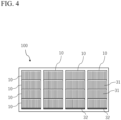
- FIG. 4 is a schematic plan view of a solar cell module including a photoelectric conversion element.
- a solar cell module 100 may include one or a plurality of photoelectric conversion elements 10. Note that Fig. 4 illustrates the photoelectric conversion module 100 including a plurality of photoelectric conversion elements 10.
- the one or the plurality of photoelectric conversion elements 10 may be sealed with, for example, a sealing material.
- the plurality of photoelectric conversion elements 10 may be disposed in at least one direction, and preferably may be disposed in a lattice pattern. In this case, the plurality of photoelectric conversion elements 10 may be electrically connected to each other in series and/or in parallel.
- the photoelectric conversion elements 10 are disposed so as to be partially overlapped each other.
- adjacent photoelectric conversion elements 10 are partially overlapped each other.
- a certain photoelectric conversion element 10 may be disposed so as to cover the second portion 32 of the collecting electrode 30 of the photoelectric conversion element 10 adjacent thereto.
- the photoelectric conversion element 10 is electrically connected to the second portion 32 of the collecting electrode 30 of the photoelectric conversion element 10 adjacent thereto.
- the photoelectric conversion elements 10 adjacent to each other may be disposed at intervals.
- the photoelectric conversion module 100 may include a conductive interconnector (not illustrated) that electrically connects the second portion 32 of the collecting electrode 30 of a certain photoelectric conversion element 10 and the photoelectric conversion element 10 adjacent thereto.
- FIG. 5 is a schematic perspective view of an artificial satellite including a solar cell module.
- An artificial satellite 900 may have a base 910 and a paddle 920.
- the base 910 may include a device (not illustrated) necessary for controlling the artificial satellite 900 and the like.
- An antenna 940 may be attached to the base 910.
- the paddle 920 may include the solar cell module 100 described above.
- the paddle 920 including the solar cell module 100 can be used as a power supply for operating various devices provided on the base 910.
- the solar cell module 100 can be applied to a paddle for an artificial satellite.
- the solar cell module 100 including the photoelectric conversion element 10 having high resistance to the temperature change described above.
- the paddle 920 may have a connection portion 922 and a hinge portion 924.
- the connection portion 922 corresponds to a portion connecting the paddle 920 to the base 910.
- the hinge portion 924 extends along one direction, and the paddle 920 can be bent with the hinge portion 924 as a rotation axis.
- Each paddle 920 may have at least one, preferably a plurality of, hinges 924.
- the paddle 920 including the solar cell module 100 is configured to be foldable small.
- the paddle 920 may be in a folded state. It is sufficient that the paddle 920 is unfolded when receiving sunlight to generate power.
- the paddle 920 may have a cylindrical shape formed by being wound. Accordingly, the paddle 920 can take a substantially flat unfolded state by a rotation of the wound portion. When the artificial satellite 900 is launched, the paddle 920 may maintain a generally cylindrical shape. It is sufficient that the paddle 920 is unfolded so as to be in a substantially flat state when receiving sunlight to generate power.
- the collecting electrode 30 is provided on the second electrode layer 24.
- the collecting electrode 30 may be provided between the photoelectric conversion layer 26 and the second electrode layer 24.
- the second electrode layer 24 may be constituted by a transparent electrode layer.
- the first electrode layer 22 may be constituted by a transparent electrode layer.
- the second electrode layer 24 may be constituted by a transparent electrode layer or an opaque electrode layer.
- the first portions 31 of all the collecting electrodes 30 formed in the same photoelectric conversion element have the same length L, width W, and thickness D.
- the plurality of first portions 31 formed in the same photoelectric conversion element may have different lengths L, widths W, and thicknesses D from each other. In this case, it is preferable that at least a part, preferably all, of the plurality of first portions 31 satisfy the above-described conditions regarding the length L, the width W, and the thickness D.
- the thin-film photoelectric conversion element has been described as an example, but the present invention is not limited thereto, and can be applied to a crystalline photoelectric conversion element as much as possible. Even in the crystalline photoelectric conversion element, an influence of the thermal stress can be alleviated by setting the conditions regarding the length L, the width W, and the thickness D of the first portion 31 of the collecting electrode 30 as described above. However, from the viewpoint of suppressing peeling of the laminated body 25, it is particularly desirable to apply the present invention to a thin-film photoelectric conversion element.
- the first portion 31 of the collecting electrode 30 has the protrusion 31a.
- the first portion 31 of the current collecting electrode 30 may have a substantially line-like shape without the protrusion 31a.
- the first portion 31 of the collecting electrode 30 extends only in one direction from the second portion 32.
- the plurality of first portions 31 may extend in different directions from each other from the second portion 32.
- the plurality of first portions 31 may extend in directions opposite to each other.
- a certain first portion 31 may extend in a direction inclined with respect to another first portion 31.
- the second portion 32 of the collecting electrode 30 extends straight in the Y direction.
- the second portion 32 of the collecting electrode 30 may extend in a wavy line shape or a zigzag polygonal line shape.
Landscapes
- Engineering & Computer Science (AREA)
- Life Sciences & Earth Sciences (AREA)
- Sustainable Development (AREA)
- Remote Sensing (AREA)
- Aviation & Aerospace Engineering (AREA)
- Photovoltaic Devices (AREA)
- Sustainable Energy (AREA)
Applications Claiming Priority (2)
| Application Number | Priority Date | Filing Date | Title |
|---|---|---|---|
| JP2021091105 | 2021-05-31 | ||
| PCT/JP2022/022062 WO2022255337A1 (ja) | 2021-05-31 | 2022-05-31 | 光電変換素子、太陽電池モジュール及びパドル |
Publications (2)
| Publication Number | Publication Date |
|---|---|
| EP4350780A1 true EP4350780A1 (de) | 2024-04-10 |
| EP4350780A4 EP4350780A4 (de) | 2025-06-11 |
Family
ID=84323288
Family Applications (1)
| Application Number | Title | Priority Date | Filing Date |
|---|---|---|---|
| EP22816083.4A Pending EP4350780A4 (de) | 2021-05-31 | 2022-05-31 | Photoelektrisches umwandlungselement, solarzellenmodul und paddel |
Country Status (5)
| Country | Link |
|---|---|
| US (1) | US20240258442A1 (de) |
| EP (1) | EP4350780A4 (de) |
| JP (1) | JPWO2022255337A1 (de) |
| CN (1) | CN117581386A (de) |
| WO (1) | WO2022255337A1 (de) |
Family Cites Families (15)
| Publication number | Priority date | Publication date | Assignee | Title |
|---|---|---|---|---|
| JP2005268466A (ja) * | 2004-03-18 | 2005-09-29 | Sanyo Electric Co Ltd | 光起電力装置 |
| JP5301758B2 (ja) * | 2005-05-19 | 2013-09-25 | 信越半導体株式会社 | 太陽電池 |
| US20100275982A1 (en) * | 2007-09-04 | 2010-11-04 | Malcolm Abbott | Group iv nanoparticle junctions and devices therefrom |
| JP2009302274A (ja) | 2008-06-13 | 2009-12-24 | Hitachi Maxell Ltd | 光発電素子、cis系光発電素子の製造方法 |
| KR20120096003A (ko) * | 2009-11-20 | 2012-08-29 | 이 아이 듀폰 디 네모아 앤드 캄파니 | 반도체 패키징 응용에 유용한 인터포저 필름, 및 그 관련 방법 |
| JP2011198883A (ja) * | 2010-03-18 | 2011-10-06 | Fujifilm Corp | 光電変換素子 |
| JP2012019094A (ja) * | 2010-07-08 | 2012-01-26 | Hitachi High-Technologies Corp | 太陽電池モジュール |
| JP5799255B2 (ja) * | 2010-11-29 | 2015-10-21 | パナソニックIpマネジメント株式会社 | 太陽電池セル及び太陽電池モジュール |
| KR20140015314A (ko) * | 2011-01-28 | 2014-02-06 | 아사히 가라스 가부시키가이샤 | Cu-In-Ga-Se 태양 전지용 유리 기판 및 그것을 사용한 태양 전지 |
| JP2013077706A (ja) * | 2011-09-30 | 2013-04-25 | Fujifilm Corp | 光電変換素子およびその製造方法 |
| EP2800144A1 (de) * | 2013-05-03 | 2014-11-05 | Saint-Gobain Glass France | Rückseitenkontaktiertes Substrat für eine Photovoltaikzelle oder ein Photovoltaikmodul |
| JP2017152661A (ja) * | 2016-02-26 | 2017-08-31 | 凸版印刷株式会社 | 化合物薄膜太陽電池、化合物薄膜太陽電池の製造方法、および、化合物薄膜太陽電池の検査方法 |
| RU2682836C1 (ru) * | 2018-05-29 | 2019-03-21 | Общество с ограниченной ответственностью "Солартек" | Способ изготовления светопроницаемого тонкопленочного солнечного модуля на основе халькопирита |
| JP7420539B2 (ja) | 2019-12-06 | 2024-01-23 | ファナック株式会社 | 射出成形機の制御装置および制御方法 |
| CN111081795B (zh) * | 2019-12-31 | 2025-05-06 | 通威太阳能(成都)有限公司 | 一种太阳能电池、组件结构及其制备方法 |
-
2022
- 2022-05-31 US US18/565,280 patent/US20240258442A1/en active Pending
- 2022-05-31 EP EP22816083.4A patent/EP4350780A4/de active Pending
- 2022-05-31 JP JP2023525840A patent/JPWO2022255337A1/ja active Pending
- 2022-05-31 WO PCT/JP2022/022062 patent/WO2022255337A1/ja not_active Ceased
- 2022-05-31 CN CN202280046358.0A patent/CN117581386A/zh active Pending
Also Published As
| Publication number | Publication date |
|---|---|
| US20240258442A1 (en) | 2024-08-01 |
| CN117581386A (zh) | 2024-02-20 |
| WO2022255337A1 (ja) | 2022-12-08 |
| EP4350780A4 (de) | 2025-06-11 |
| JPWO2022255337A1 (de) | 2022-12-08 |
Similar Documents
| Publication | Publication Date | Title |
|---|---|---|
| JP3658160B2 (ja) | モールドレス半導体装置 | |
| KR20240017894A (ko) | 태양 전지 | |
| WO2008036769A2 (en) | Semi-transparent dual layer back contact for bifacial and tandem junction thin-film photovolataic devices | |
| KR20140003691A (ko) | 태양 전지 모듈 및 이에 적용되는 리본 결합체 | |
| EP2426731A2 (de) | Vorrichtung zur solarstromerzeugung sowie verfahren zu ihrer herstellung | |
| KR20120063324A (ko) | 양면 태양전지 | |
| US20130319502A1 (en) | Bifacial Stack Structures for Thin-Film Photovoltaic Cells | |
| EP2224491A2 (de) | Solarzelle und Verfahren zu deren Herstellung | |
| US20150059838A1 (en) | Solar cell apparatus and method of fabricating the same | |
| US20170323986A1 (en) | Photovoltaic module | |
| KR101428146B1 (ko) | 태양전지 모듈 및 이의 제조방법 | |
| EP4350780A1 (de) | Photoelektrisches umwandlungselement, solarzellenmodul und paddel | |
| EP2450968B1 (de) | Photovoltaikvorrichtung | |
| US12532550B2 (en) | Photoelectric conversion module, paddle, and method for manufacturing photoelectric conversion module | |
| US20120240980A1 (en) | Interconnection Schemes for Photovoltaic Cells | |
| US20240178338A1 (en) | Photoelectric conversion element and method for manufacturing photoelectric conversion element | |
| EP4293731A1 (de) | Solarzelle, mehrfachsolarzelle, solarzellenmodul und solarstromerzeugungssystem | |
| JP2008218937A (ja) | 小型(小面積)のcis系薄膜太陽電池モジュール | |
| EP4365959A1 (de) | Photoelektrisches umwandlungselement und verfahren zur herstellung eines photoelektrischen umwandlungselements | |
| EP2608273A2 (de) | Solarzelle mit einem PN-Heteroübergang | |
| US20250011010A1 (en) | Photoelectric conversion module, paddle, and method for manufacturing photoelectric conversion module | |
| US20250234656A1 (en) | Photoelectric conversion module, paddle, and method for manufacturing photoelectric conversion module | |
| KR20180055542A (ko) | 태양 전지 패널 및 이의 제조 방법 | |
| EP4693418A1 (de) | Photoelektrisches umwandlungselement, photovoltaisches modul, flugobjekt und verfahren zur herstellung eines photoelektrischen umwandlungselements | |
| EP4250376A1 (de) | Solarzellen und herstellungsverfahren davon |
Legal Events
| Date | Code | Title | Description |
|---|---|---|---|
| STAA | Information on the status of an ep patent application or granted ep patent |
Free format text: STATUS: THE INTERNATIONAL PUBLICATION HAS BEEN MADE |
|
| PUAI | Public reference made under article 153(3) epc to a published international application that has entered the european phase |
Free format text: ORIGINAL CODE: 0009012 |
|
| STAA | Information on the status of an ep patent application or granted ep patent |
Free format text: STATUS: REQUEST FOR EXAMINATION WAS MADE |
|
| 17P | Request for examination filed |
Effective date: 20231220 |
|
| AK | Designated contracting states |
Kind code of ref document: A1 Designated state(s): AL AT BE BG CH CY CZ DE DK EE ES FI FR GB GR HR HU IE IS IT LI LT LU LV MC MK MT NL NO PL PT RO RS SE SI SK SM TR |
|
| DAV | Request for validation of the european patent (deleted) | ||
| DAX | Request for extension of the european patent (deleted) | ||
| REG | Reference to a national code |
Ref country code: DE Ref legal event code: R079 Free format text: PREVIOUS MAIN CLASS: H01L0031022400 Ipc: H10F0077200000 |
|
| A4 | Supplementary search report drawn up and despatched |
Effective date: 20250512 |
|
| RIC1 | Information provided on ipc code assigned before grant |
Ipc: B64G 1/44 20060101ALI20250506BHEP Ipc: H10F 19/90 20250101ALI20250506BHEP Ipc: H10F 10/167 20250101ALI20250506BHEP Ipc: H10F 77/20 20250101AFI20250506BHEP |