EP4350919A2 - Verfahren und schaltungsanordnung zum einschalten einer elektrischen schaltung - Google Patents
Verfahren und schaltungsanordnung zum einschalten einer elektrischen schaltung Download PDFInfo
- Publication number
- EP4350919A2 EP4350919A2 EP23200823.5A EP23200823A EP4350919A2 EP 4350919 A2 EP4350919 A2 EP 4350919A2 EP 23200823 A EP23200823 A EP 23200823A EP 4350919 A2 EP4350919 A2 EP 4350919A2
- Authority
- EP
- European Patent Office
- Prior art keywords
- voltage
- circuit
- value
- power transistor
- pulse signal
- Prior art date
- Legal status (The legal status is an assumption and is not a legal conclusion. Google has not performed a legal analysis and makes no representation as to the accuracy of the status listed.)
- Granted
Links
Images



Classifications
-
- G—PHYSICS
- G11—INFORMATION STORAGE
- G11C—STATIC STORES
- G11C11/00—Digital stores characterised by the use of particular electric or magnetic storage elements; Storage elements therefor
- G11C11/21—Digital stores characterised by the use of particular electric or magnetic storage elements; Storage elements therefor using electric elements
- G11C11/34—Digital stores characterised by the use of particular electric or magnetic storage elements; Storage elements therefor using electric elements using semiconductor devices
- G11C11/40—Digital stores characterised by the use of particular electric or magnetic storage elements; Storage elements therefor using electric elements using semiconductor devices using transistors
- G11C11/401—Digital stores characterised by the use of particular electric or magnetic storage elements; Storage elements therefor using electric elements using semiconductor devices using transistors forming cells needing refreshing or charge regeneration, i.e. dynamic cells
- G11C11/4063—Auxiliary circuits, e.g. for addressing, decoding, driving, writing, sensing or timing
- G11C11/407—Auxiliary circuits, e.g. for addressing, decoding, driving, writing, sensing or timing for memory cells of the field-effect type
- G11C11/4074—Power supply or voltage generation circuits, e.g. bias voltage generators, substrate voltage generators, back-up power, power control circuits
-
- H—ELECTRICITY
- H03—ELECTRONIC CIRCUITRY
- H03K—PULSE TECHNIQUE
- H03K17/00—Electronic switching or gating, i.e. not by contact-making and –breaking
- H03K17/08—Modifications for protecting switching circuit against overcurrent or overvoltage
- H03K17/081—Modifications for protecting switching circuit against overcurrent or overvoltage without feedback from the output circuit to the control circuit
- H03K17/08104—Modifications for protecting switching circuit against overcurrent or overvoltage without feedback from the output circuit to the control circuit in field-effect transistor switches
-
- G—PHYSICS
- G11—INFORMATION STORAGE
- G11C—STATIC STORES
- G11C11/00—Digital stores characterised by the use of particular electric or magnetic storage elements; Storage elements therefor
- G11C11/21—Digital stores characterised by the use of particular electric or magnetic storage elements; Storage elements therefor using electric elements
- G11C11/34—Digital stores characterised by the use of particular electric or magnetic storage elements; Storage elements therefor using electric elements using semiconductor devices
- G11C11/40—Digital stores characterised by the use of particular electric or magnetic storage elements; Storage elements therefor using electric elements using semiconductor devices using transistors
- G11C11/401—Digital stores characterised by the use of particular electric or magnetic storage elements; Storage elements therefor using electric elements using semiconductor devices using transistors forming cells needing refreshing or charge regeneration, i.e. dynamic cells
- G11C11/4063—Auxiliary circuits, e.g. for addressing, decoding, driving, writing, sensing or timing
- G11C11/407—Auxiliary circuits, e.g. for addressing, decoding, driving, writing, sensing or timing for memory cells of the field-effect type
- G11C11/4072—Circuits for initialization, powering up or down, clearing memory or presetting
-
- G—PHYSICS
- G11—INFORMATION STORAGE
- G11C—STATIC STORES
- G11C11/00—Digital stores characterised by the use of particular electric or magnetic storage elements; Storage elements therefor
- G11C11/21—Digital stores characterised by the use of particular electric or magnetic storage elements; Storage elements therefor using electric elements
- G11C11/34—Digital stores characterised by the use of particular electric or magnetic storage elements; Storage elements therefor using electric elements using semiconductor devices
- G11C11/40—Digital stores characterised by the use of particular electric or magnetic storage elements; Storage elements therefor using electric elements using semiconductor devices using transistors
- G11C11/401—Digital stores characterised by the use of particular electric or magnetic storage elements; Storage elements therefor using electric elements using semiconductor devices using transistors forming cells needing refreshing or charge regeneration, i.e. dynamic cells
- G11C11/4063—Auxiliary circuits, e.g. for addressing, decoding, driving, writing, sensing or timing
- G11C11/407—Auxiliary circuits, e.g. for addressing, decoding, driving, writing, sensing or timing for memory cells of the field-effect type
- G11C11/409—Read-write [R-W] circuits
- G11C11/4096—Input/output [I/O] data management or control circuits, e.g. reading or writing circuits, I/O drivers or bit-line switches
-
- H—ELECTRICITY
- H02—GENERATION; CONVERSION OR DISTRIBUTION OF ELECTRIC POWER
- H02H—EMERGENCY PROTECTIVE CIRCUIT ARRANGEMENTS
- H02H9/00—Emergency protective circuit arrangements for limiting excess current or voltage without disconnection
- H02H9/001—Emergency protective circuit arrangements for limiting excess current or voltage without disconnection limiting speed of change of electric quantities, e.g. soft switching on or off
-
- H—ELECTRICITY
- H02—GENERATION; CONVERSION OR DISTRIBUTION OF ELECTRIC POWER
- H02M—APPARATUS FOR CONVERSION BETWEEN AC AND AC, BETWEEN AC AND DC, OR BETWEEN DC AND DC, AND FOR USE WITH MAINS OR SIMILAR POWER SUPPLY SYSTEMS; CONVERSION OF DC OR AC INPUT POWER INTO SURGE OUTPUT POWER; CONTROL OR REGULATION THEREOF
- H02M1/00—Details of apparatus for conversion
- H02M1/32—Means for protecting converters other than automatic disconnection
-
- H—ELECTRICITY
- H02—GENERATION; CONVERSION OR DISTRIBUTION OF ELECTRIC POWER
- H02M—APPARATUS FOR CONVERSION BETWEEN AC AND AC, BETWEEN AC AND DC, OR BETWEEN DC AND DC, AND FOR USE WITH MAINS OR SIMILAR POWER SUPPLY SYSTEMS; CONVERSION OF DC OR AC INPUT POWER INTO SURGE OUTPUT POWER; CONTROL OR REGULATION THEREOF
- H02M1/00—Details of apparatus for conversion
- H02M1/36—Means for starting or stopping converters
-
- H—ELECTRICITY
- H03—ELECTRONIC CIRCUITRY
- H03K—PULSE TECHNIQUE
- H03K17/00—Electronic switching or gating, i.e. not by contact-making and –breaking
- H03K17/08—Modifications for protecting switching circuit against overcurrent or overvoltage
- H03K17/082—Modifications for protecting switching circuit against overcurrent or overvoltage by feedback from the output to the control circuit
- H03K17/0822—Modifications for protecting switching circuit against overcurrent or overvoltage by feedback from the output to the control circuit in field-effect transistor switches
Definitions
- the present description generally relates to a method and a circuit for powering up an electrical circuit comprising a high capacitive load.
- electrical circuits include significant capacitive loads that must be charged when the circuits are powered up.
- the capacitive load is supplied for example from a battery and via a power transistor.
- the capacitive loads include devices to be powered, which may be associated with capacitances, and also include capacitive conductors that connect the power transistor to the devices to be powered. It is desirable that the loading of the capacitive loads of the circuit be relatively rapid so that the devices are operational in a relatively short time.
- the application of a high current density on the power transistor when powering an electrical circuit allows rapid charging of capacitive loads.
- high current density may be seen by the circuit as being due to a short circuit, and therefore triggers protection mechanisms.
- the application of high current density fatigues certain components, including the power transistor.
- One embodiment overcomes all or part of the drawbacks of known loading methods.
- the threshold level corresponds to a current level for which the thermal coefficient of the power transistor is negative.
- At least one value among: the first voltage threshold value; the value of the first rest time; and the value of the second rest time is determined by a value stored in a programmable memory of the circuit.
- the comparator is further configured to, following one or more of the pulses of the second signal, carrying out a second comparison of the voltage value across the capacitive load with the first voltage threshold value and in which the control circuit is further configured to, if during the second comparison the voltage value is less than or equal to the first voltage threshold value, stop the first pulse signal.
- the transformer and the switch box are part of an automobile.
- the expressions “approximately”, “approximately”, “substantially”, and “of the order of” mean to the nearest 10%, preferably to the nearest 5%.
- FIG. 1 is a block diagram illustrating a system 100 configured to power capacitive loads 104 and 108 of an electrical circuit according to one embodiment of the present description.
- the system 100 is for example part of a larger device (not shown), such as for example the electrical system of an automobile, having a high capacitive load.
- the capacitive load 104 represented by a capacitor connected to ground (GND)
- the capacitive load 108 which is represented by another capacitor connected to ground (GND )
- GND ground
- the capacitive load 108 is powered by a second rail 110.
- the system 100 includes a greater number of capacitive loads, each powered by a corresponding rail.
- the system 100 further comprises a switching box 112, as well as a transformer 114 (DC/DC) configured to power the switching box 112 by applying a voltage Vbat to it.
- transformer 114 receives an input DC voltage from a DC source (not shown in the figure). figure 1 ), such as a battery, and generates the voltage Vbat having a voltage level different from the input DC voltage.
- a DC source not shown in the figure.
- figure 1 such as a battery
- transformer 114 is not present, and switch box 112 is powered directly from the battery.
- the switching box 112 comprises for example an electrical circuit 116 (E-FUSE) configured to, for example, power the rails 106 and 110 via one or more power transistors.
- E-FUSE electrical circuit 116
- the switching box 112 further comprises, for example, a processing unit 118 (MCU) configured to control the electrical circuit 116, for example in order to manage the power supply of different components powered by the circuit 116.
- MCU processing unit 118
- the system 100 for example further comprises a circuit 120 coupled to the switching box 112 via the rails 106 and 110.
- the circuit 120 comprises for example a processing unit 122 (MCU) as well as electrical circuits 124.
- MCU processing unit
- circuit 120 is a device comprising one or more other electrical circuits.
- Circuit 120 supplies, for example, other loads 126 and 128 (LOAD) coupled to ground (GND).
- the circuit 116 is then controlled to supply the rails 106 and 110 by applying a voltage VbatA and VbatB to them respectively. Initially, the capacitive loads 104 and 108 are charged so that all of the circuits powered by the rails 106, 110 are functional, including the circuit 120. It is therefore desirable that the capacitive loads 104 and 108 are charged quickly .
- the total capacitive load of the system 100 has a high capacitance, for example a capacitance greater than 1 mF (milli-Farad).
- a high current density at the output of the switching box 112 on the rails 106 and 110 makes it possible to quickly charge the capacitive loads 104 and 108 but can fatigue and/or degrade certain components, such as power transistors and/or or printed circuits. Additionally, the application of a high current may be seen by the device as being due to a short circuit, and therefore triggers protection mechanisms.
- FIG. 2 illustrates a circuit 200 included in the circuit 116 of the switching box 112 of the figure 1 according to one embodiment of the present description.
- Circuit 200 of the figure 2 is configured to power the rail 106.
- a circuit similar to circuit 200 is for example also present in the switching box 112 to power the rail 110.
- the circuit 200 includes a power transistor 202 whose drain is for example coupled to the voltage rail supplied by the transformer 114 applying the voltage Vbat to it.
- the source of the power transistor 200 is coupled to the rail 106 and applies a voltage VbatA to it.
- the power transistor 202 comprises for example a plurality of transistors in parallel, two of which are illustrated in the figure 2 with references 204 and 210.
- the transistors 204 and 210 included in the power transistor 202 are N-channel transistors (NMOS) of the MOSFET (Metal Oxide Semiconductor Field Effect Transistor) type.
- NMOS N-channel transistors
- MOSFET Metal Oxide Semiconductor Field Effect Transistor
- the circuit 200 further comprises a control circuit 206 (FSM) coupled to the gate of the power transistor 202.
- the control circuit 206 is implemented for example by a finite state machine.
- the control circuit 206 receives, for example, a CHANNEL_ON signal indicating when the rail 106 is to be powered.
- the CHANNEL_ON signal is generated by the processing unit 118.
- the circuit 200 further comprises a detection circuit 208 (I DET.), for example arranged to connect the drain of the power transistor 210 to the rail 106.
- An output of the detection circuit 208 is for example connected to the control circuit 206.
- the detection circuit 208 is for example configured to compare the current flowing through the transistor 210 with a threshold current.
- the transistor 210 is for example of a relatively small size compared to the overall size of the power transistor 202, and therefore only conducts a relatively small part of the total current supplied by the power transistor 202.
- the current level detected by the detection circuit 208 is nevertheless proportional to the total current conducted by the power transistor 202.
- the threshold current corresponds to a current density in the power transistor 202 for which the power transistor 202 is in a state thermal stability.
- FIG. 3 is a graph 300 illustrating a thermal stability zone 302 and thermal instability zones 304 and 306 of a power transistor such as the transistor 202 of the figure 2 .
- Zone 304 corresponds to example to a first level of instability of the power transistor
- zone 306 corresponds for example to a level of increased instability for which a thermal runaway phenomenon takes place.
- the thermal coefficient of the power transistor 200 defined as the variation of the current as a function of the temperature, is negative for zone 302 and is positive for zones 304 and 306.
- graph 300 presents five curves 308 to 316 illustrating the relationship between the voltage V DS between the drain and the source of the transistor and the current I DS circulating between the drain and the source for different voltage values V GS between the gate and the source of the transistor and at different temperatures.
- Curves 308 and 310 respectively illustrate the relationship V DS and I DS when the voltage V GS is equal to 3 V and at temperatures of 25°C and 125°C.
- the current I DS increases linearly with the voltage V DS then the growth is quickly slowed down when the power transistor is saturated.
- the current I DS remains relatively low and the transistor 210 first enters the instability zone 304, for example when the voltage V DS is in a first voltage range, then in the instability zone 306, for example when the voltage V DS exceeds the upper limit of the first voltage range.
- the phenomenon of thermal runaway takes place, leading for example to current focusing problems and the formation of hot spots permanently degrading the power transistor 202.
- Curve 312 represents the relationship between the current I DS and the voltage V DS when the voltage V GS is equal to 6 V and at temperatures of 25°C and 125°C. In this example, curve 312 passes between zones 304 and 302.
- Curves 314 and 316 respectively illustrate the relationship V DS and I DS when the voltage V GS is equal to 8 V and at temperatures of 125°C and 25°C.
- the elbow of curves 314 and 316 separating the zone of linear growth between current I DS and the voltage V DS and the saturation zone in which the current I DS increases less rapidly, appears for a value of the current I DS much higher than for curves 308 and 310.
- the saturation of the power transistor takes place when the current I DS is large enough to place the power transistor in the zone of thermal stability.
- the control circuit 206 is configured to apply voltage pulse signals to the gate of the power transistor 202. Each reception of a voltage pulse places the transistors 204 and 210 in the state passing, thus allowing the charging, with a high current density during at least part of the pulse, of the capacitive load 104.
- the detection circuit 208 is configured to activate an over current signal OC to the control circuit 206, and the control circuit 206 is configured to control, in response to the signal OC, the transition of the transistors 204 and 210 to the state blocking.
- the control circuit 206 is further configured to return the transistors 204 and 210 to the on state following a rest time, thus allowing a new pulse of the pulse signal.
- the rest time allows the transistor to power 202 to, for example, cool sufficiently so as not to overheat.
- the circuit 200 comprises a comparator 212 configured to compare the voltage VbatA on the rail 106 with a voltage threshold value V out_th .
- the comparator 212 is further configured to transmit a signal VOUT_EN to the control circuit 206 when the value of the voltage VbatA reaches the voltage threshold value V out_th .
- the comparison is for example carried out continuously.
- the comparator 212 is configured to compare the values of the voltages VbatA and V out_th periodically, for example following a given number of consecutive pulses.
- FIG. 4 is a flowchart illustrating steps of a method of powering up the electrical circuit 200 supplying the rail 106, according to one embodiment of the present description.
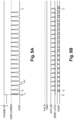
- THE figures 5A And 6A are time graphs illustrating the current density conducted by the power transistor 202 according to one embodiment of the present description.
- THE figures 5B And 6B are time graphs illustrating the evolution of the voltage VbatA according to one embodiment of the present description.
- circuit 200 is not powered by transformer 112. Power transistor 202 is therefore not powered and does not power rail 106.
- the switching box 112 includes a counter (not illustrated in figure 2 ) configured to increment a COUNT count value which is for example initialized to the value 0 when circuit 200 is not powered.
- the method of powering up circuit 116 is broken down into two phases.
- a first phase for example composed of a series of steps 401 to 405, corresponding to a supply of the rail 106 with a relatively low frequency pulse signal.
- the first phase is followed by a second phase, for example composed of a series of steps 401' to 405', corresponding to a supply of the rail 106 with a pulse signal at relatively high frequency, that is to say at a pulse frequency higher than that of the relatively low frequency pulse signal.
- switching on the circuit 200 causes for example the reception, at a time t 0 , of the signal CHANNEL_ON, for example transmitted by the processing unit 118 to the control circuit 206.
- step 401 (START LOW FREQ) of the figure 4 , beginning at time t 0 upon receipt of the CHANNEL_ON signal, the control circuit 206 sends a voltage edge to the power transistor 202 in order to place it in the on state.
- this voltage front is for example a falling edge.
- this voltage front is for example a rising edge.
- the power transistor 202 remains in the on state until the detection circuit 208 sends the signal OC to the control circuit 206, signaling that the current ILOAD passing through the power transistor 202 has reached a threshold value OVER_CURRENT.
- the threshold value is stored in a programmable memory of circuit 200 coupled to the detection circuit 208.
- the generation of the signal OC takes place for example at a time t 1 .
- the control circuit 206 is further configured to apply another voltage edge to the power transistor 202 in order to place it in the blocking state. In the case where the power transistor is implemented by a P-channel transistor, this voltage front is for example a rising edge. Following the transition of the power transistor 202 to the blocking state, the current ILOAD decreases continuously until it becomes zero.
- a stopwatch, or a time unit counter, of circuit 200 is triggered.
- the stopwatch is for example configured to time a first period of time.
- the first period of time is of the order of 4 ms.
- the timer is further configured to signal the control circuit 206 that the first period of time has elapsed since the reception of the signal OC, when this is the case.
- the first period of time is programmable.
- a value representing the first period of time is stored in the programmable memory, and the stopwatch is configured to read this value from the programmable memory and to signal to the control circuit 206 when this period of time has elapsed.
- the first period of time fixes for example a rest time t rep 1 between the pulses during the first phase.
- the control circuit 206 checks, in a step 403 (VbatA ⁇ V out_th ?), on the basis of the output signal of the comparator 212, if the value of the voltage VbatA is lower to the voltage threshold value V out_th .
- the voltage threshold value V out_th is stored in the programmable memory and is converted by a digital-to-analog converter to the analog voltage V out_th .
- Step 403 further includes incrementing the count value COUNT.
- the counting value COUNT is compared, for example by the processing unit 118, with a first maximum value. If the counting value COUNT is not equal to the first maximum value (branch N), the process continues in step 405 (RESET OVERCURRENT). For example, the first maximum value is stored in the programmable memory.
- step 405 takes place at a time t 2 .
- step 405 the control circuit 206 generates a RESET LATCH signal controlling the resetting of the detection circuit 208, and therefore the resetting of the current overflow signal OC.
- the RESET LATCH signal forces the resetting of the overflow signal OC
- the RESET LATCH signal remains active for a relatively short period of time before being extinguished, this period of time being chosen to be less than the rise time of current peaks.
- the RESET LATCH signal remains active for a time, for example less than 20us and preferably less than 10us.
- the RESET LATCH signal is a non-priority signal with respect to the detection of current overrun by the detection circuit 208. In this case, if the detection circuit 208 detects a current overrun while the RESET signal LATCH is active, the circuit detection 208 nevertheless activates the current excess signal OC. The process then resumes at step 401.
- the method continues thus, in a series of executions of steps 401 to 405, until a realization of step 405, at a time t 3 , in which the counting value COUNT reaches the maximum value (branch N at output of step 404).
- the maximum value is for example equal to 20. However, any other integer value is possible as a maximum value. In this case, the process ends in step 406 (STOP).
- Step 406 then consists, for example, of switching off circuit 116 or switching box 112.
- the voltage VbatA reaches the voltage threshold value V out_th (branch N at the output of step 403) at a time t 4 .
- the count value is then equal to 4 and is less than the maximum value. As the voltage VbatA reaches the voltage threshold value relatively quickly, this indicates that the rail 106 is correctly powered and that no short circuit occurs.
- step 403 it is determined that the rail 106 is correctly powered and that the power transistor 202 supports the power supply and is not short-circuited, the rest time between two voltage pulses is reduced , and/or the pulse duty cycle is increased, in order to accelerate the increase in tension on rail 106.
- the counting value COUNT is reset, for example to 0.
- step 405' RESET OVERCURRENT
- step 405' RESET OVERCURRENT
- Step 401' (START HIGH FREQ) is similar to step 401 and consists of the application, by the control circuit 206, of a voltage front making the power transistor 202 on. The control circuit 206 then applies another voltage front, turning the power transistor 202 off, upon reception of the signal OC.
- Step 402' (COUNT HIGH FREQUENCY) is similar to step 402 except that the timer is configured to signal to the control circuit 206 that a second period of time has elapsed since the reception of the signal OC, when it's the case.
- the value of the second period of time is for example stored in the programmable memory. Additionally, the value of the second time frame is less than the value of the first time frame.
- the second period of time is for example of the order of 1 ms.
- the second period of time fixes for example a rest time t rep 2 between the pulses during the second phase, the rest time t rep 2 being less than the rest time t rep 1 .
- the rest time of the power transistor 202 between its transition to the blocking state and the moment when it is returned to the on state is faster than during the first power phase.
- the loading of the capacitive load 104 is then accelerated.
- Step 403' is similar to step 403.
- step 403' the comparator 212 determines that the voltage VbatA becomes lower than the voltage threshold value V out_th (branch Y), the process ends at step 406. Indeed, if the voltage VbatA becomes lower than the threshold value V out_th again, a problem, such as for example a short circuit, occurs for example in the system 100.
- the second maximum value is for example stored in the programmable memory. In another example, the second maximum value is equal to the first maximum value and steps 404' and 404 are identical.
- step 404' if during step 404' the counting value is equal to the second maximum value (branch Y), this means that recharging the capacitive load 104 takes too long and that an anomaly occurs. The process then ends in step 406.
- step 404' If, in step 404', the counting value is not equal to the second maximum value (branch N), the process resumes in step 401'.
- the sequence of steps 401' to 405' is carried out up to a time t 5 , taking place for example during the carrying out of step 401'.
- the instant t 5 corresponds to the instant when the capacitive load 104 is completely charged, and the voltage VbatA then remains constant.
- the control circuit 206 is further configured to detect the instant when the capacitive load 104 is fully charged and to, for example, leave the transistor 202 in the on state in order to continuously power the devices such as for example the circuit 120.
- the circuit 200 comprises another comparator configured to compare the voltage VbatA with a maximum voltage Vmax corresponding to the voltage on the rail 106 when the capacitive load 104 is fully charged. For example, the value of the voltage Vmax is stored in the programmable memory.
- the rail 106 is supplied with a signal at a first voltage pulse frequency, applied by the control circuit 206.
- the signal at the first pulse frequency is transmitted between the times t 0 and t 4 .
- the rail 106 is then supplied with a new signal, at a second pulse frequency higher than the first frequency, emitted by the control circuit 206 between times t 4 and t 5 .
- the rest time t rep 1 between each pulse of the signal at the first voltage pulse frequency is greater than the rest time t rep 2 between each pulse of the signal at the second pulse frequency.
- the rest time between two pulses corresponds, for example, to the time between the end of one pulse and the start of the next pulse.
- the duration of a current pulse varies relatively little during the charging of the capacitive load 104.
- the voltage pulses of the signal at the first frequency then have, for example, a duration similar to the voltage pulses of the signal at the first frequency. second frequency.
- the duty cycle of the signal at the first pulse frequency is, for example, smaller than the duty cycle of the signal at the second pulse frequency.
- the circuit 200 comprises, in addition to the detection circuit 208, or instead of the detection circuit 208, a thermal detector configured to compare the temperature of circuit 200, and more particularly the temperature of power transistor 202, with a threshold temperature.
- the thermal detector is for example coupled to the control circuit 206 and further configured to transmit a signal to it when the measured temperature exceeds the threshold temperature.
- the control circuit 206 is for example configured to cut off the power supply to the power transistor 202 upon receipt of the signal transmitted by the thermal detector.
- An advantage of the embodiments described is that they allow rapid loading of the capacitive loads of a circuit, while monitoring the risks of short circuit and avoiding placing the power transistor in a state of thermal instability.
- the current being a continuous value and the current pulse supplied by the power transistor starting from 0, the power transistor automatically has a transition phase in a thermal instability zone.
- the time spent in the thermal instability zone is negligible compared to the thermal constants and does not give the power transistor time to degrade.
- Another advantage of the embodiments described is that the rest time between pulses decreases, and/or the duty cycle of the pulse signal increases, when the risk of short circuit is eliminated.
- Another advantage of the embodiments described is that powering the rails with pulse signals interspersed with rest times allows the power transistor 202 not to overheat and to support power supply with a high current but in a discontinuous manner. .
- a counter and a count value can be used during the first power phase and another counter, incrementing another count value, or alternatively, the same counter incrementing the other count value, can be used during the second feeding phase.
Landscapes
- Engineering & Computer Science (AREA)
- Microelectronics & Electronic Packaging (AREA)
- Computer Hardware Design (AREA)
- Power Engineering (AREA)
- Databases & Information Systems (AREA)
- Electronic Switches (AREA)
- Direct Current Feeding And Distribution (AREA)
- Power Conversion In General (AREA)
Applications Claiming Priority (1)
| Application Number | Priority Date | Filing Date | Title |
|---|---|---|---|
| FR2210275A FR3140720A1 (fr) | 2022-10-07 | 2022-10-07 | Procédé et circuit de mise sous tension d’un circuit électrique |
Publications (3)
| Publication Number | Publication Date |
|---|---|
| EP4350919A2 true EP4350919A2 (de) | 2024-04-10 |
| EP4350919A3 EP4350919A3 (de) | 2024-06-05 |
| EP4350919B1 EP4350919B1 (de) | 2026-05-06 |
Family
ID=85018302
Family Applications (1)
| Application Number | Title | Priority Date | Filing Date |
|---|---|---|---|
| EP23200823.5A Active EP4350919B1 (de) | 2022-10-07 | 2023-09-29 | Verfahren und schaltungsanordnung zum einschalten einer elektrischen schaltung |
Country Status (3)
| Country | Link |
|---|---|
| US (1) | US12488829B2 (de) |
| EP (1) | EP4350919B1 (de) |
| FR (1) | FR3140720A1 (de) |
Family Cites Families (10)
| Publication number | Priority date | Publication date | Assignee | Title |
|---|---|---|---|---|
| US7064946B2 (en) | 2003-12-18 | 2006-06-20 | International Rectifier Corporation | Electronic fuse |
| US8299767B1 (en) | 2006-08-18 | 2012-10-30 | Picor Corporation | Dynamic safe operating area control |
| US9787085B2 (en) * | 2014-04-18 | 2017-10-10 | International Business Machines Corporation | Hot plug device providing turn on FETs with a softstart capability |
| US9306559B2 (en) * | 2014-04-18 | 2016-04-05 | International Business Machines Corporation | Controlling turn on FETs of a hot plug device |
| US9712061B1 (en) * | 2016-08-30 | 2017-07-18 | Silanna Asia Pte Ltd | Power converter overvoltage system |
| EP3499669A1 (de) * | 2017-12-13 | 2019-06-19 | Ovh | Schaltung und system zur implementierung einer intelligenten sicherung für eine stromversorgung |
| US10558230B2 (en) * | 2018-02-09 | 2020-02-11 | Nvidia Corp. | Switched low-dropout voltage regulator |
| US11411497B2 (en) * | 2020-08-18 | 2022-08-09 | Nxp Usa, Inc. | Switching power regulator and method for recovering the switching power regulator from an unregulated state |
| US11611277B2 (en) * | 2020-09-30 | 2023-03-21 | Airoha Technology Corp. | Soft-start method for a switching regulator |
| JP2024052412A (ja) * | 2022-09-30 | 2024-04-11 | ラピステクノロジー株式会社 | 半導体装置、レギュレータ回路、レギュレータ回路を起動する方法 |
-
2022
- 2022-10-07 FR FR2210275A patent/FR3140720A1/fr active Pending
-
2023
- 2023-09-13 US US18/466,283 patent/US12488829B2/en active Active
- 2023-09-29 EP EP23200823.5A patent/EP4350919B1/de active Active
Also Published As
| Publication number | Publication date |
|---|---|
| US20240119992A1 (en) | 2024-04-11 |
| EP4350919A3 (de) | 2024-06-05 |
| FR3140720A1 (fr) | 2024-04-12 |
| US12488829B2 (en) | 2025-12-02 |
| EP4350919B1 (de) | 2026-05-06 |
Similar Documents
| Publication | Publication Date | Title |
|---|---|---|
| EP3945673B1 (de) | Spannungsvergleicher | |
| EP4037170B1 (de) | Synchronisierung einer elektronischen vorrichtung | |
| FR2908943A1 (fr) | Circuit d'alimentation d'amplification de commutation | |
| FR2756984A1 (fr) | Alimentation de secours destinee a suppleer provisoirement a une carence d'une source d'alimentation principale | |
| FR3102620A1 (fr) | Convertisseur de tension | |
| EP3945674A1 (de) | Spannungswandler | |
| FR3102900A1 (fr) | Convertisseur de tension | |
| EP4350919A2 (de) | Verfahren und schaltungsanordnung zum einschalten einer elektrischen schaltung | |
| EP4068606B1 (de) | Spannungswandler | |
| FR3026900A1 (de) | ||
| EP4044415A1 (de) | Starten einer stromzuführung mit partitionierung | |
| EP3633487A1 (de) | Schaltwandler | |
| FR3119499A1 (fr) | Synchronisation d'un dispositif électronique | |
| EP3771080A1 (de) | Starten eine stromzuführung mit partitionierung | |
| FR2913828A1 (fr) | Convertisseur dc/dc commande par modulation de largeur d'impulsion, avec un rendement eleve a faible courant de sortie | |
| FR2971379A1 (fr) | Commande a hysteresis d'un dispositif electronique par un signal module en largeur d'impulsion | |
| EP4092892A1 (de) | Schaltnetzteil | |
| EP3826158B1 (de) | Schaltersteuerung | |
| WO2020011768A1 (fr) | Procede de declenchement de la mise a l'etat passant d'un transistor | |
| EP4346077B1 (de) | Transistorsteuerung | |
| FR2535551A1 (fr) | Dispositif de commutation electronique a faible dissipation de puissance | |
| EP4089906A1 (de) | Dc-dc-abwärtswandler mit abschaltfunktion | |
| FR3113140A1 (fr) | Convertisseur de tension | |
| EP4593271A1 (de) | Schaltnetzteil | |
| EP4593270A1 (de) | Schaltnetzteil |
Legal Events
| Date | Code | Title | Description |
|---|---|---|---|
| PUAI | Public reference made under article 153(3) epc to a published international application that has entered the european phase |
Free format text: ORIGINAL CODE: 0009012 |
|
| STAA | Information on the status of an ep patent application or granted ep patent |
Free format text: STATUS: REQUEST FOR EXAMINATION WAS MADE |
|
| 17P | Request for examination filed |
Effective date: 20230929 |
|
| AK | Designated contracting states |
Kind code of ref document: A2 Designated state(s): AL AT BE BG CH CY CZ DE DK EE ES FI FR GB GR HR HU IE IS IT LI LT LU LV MC ME MK MT NL NO PL PT RO RS SE SI SK SM TR |
|
| PUAL | Search report despatched |
Free format text: ORIGINAL CODE: 0009013 |
|
| AK | Designated contracting states |
Kind code of ref document: A3 Designated state(s): AL AT BE BG CH CY CZ DE DK EE ES FI FR GB GR HR HU IE IS IT LI LT LU LV MC ME MK MT NL NO PL PT RO RS SE SI SK SM TR |
|
| RIC1 | Information provided on ipc code assigned before grant |
Ipc: H02M 1/32 20070101ALI20240502BHEP Ipc: H03K 17/082 20060101ALI20240502BHEP Ipc: H03K 17/081 20060101ALI20240502BHEP Ipc: H02M 1/36 20070101ALI20240502BHEP Ipc: H02H 9/00 20060101AFI20240502BHEP |
|
| GRAP | Despatch of communication of intention to grant a patent |
Free format text: ORIGINAL CODE: EPIDOSNIGR1 |
|
| STAA | Information on the status of an ep patent application or granted ep patent |
Free format text: STATUS: GRANT OF PATENT IS INTENDED |
|
| INTG | Intention to grant announced |
Effective date: 20251203 |
|
| GRAS | Grant fee paid |
Free format text: ORIGINAL CODE: EPIDOSNIGR3 |
|
| GRAA | (expected) grant |
Free format text: ORIGINAL CODE: 0009210 |
|
| STAA | Information on the status of an ep patent application or granted ep patent |
Free format text: STATUS: THE PATENT HAS BEEN GRANTED |