EP4350966A1 - Schaltwandler mit teilleistungsverarbeitung - Google Patents
Schaltwandler mit teilleistungsverarbeitung Download PDFInfo
- Publication number
- EP4350966A1 EP4350966A1 EP22199709.1A EP22199709A EP4350966A1 EP 4350966 A1 EP4350966 A1 EP 4350966A1 EP 22199709 A EP22199709 A EP 22199709A EP 4350966 A1 EP4350966 A1 EP 4350966A1
- Authority
- EP
- European Patent Office
- Prior art keywords
- value
- converter
- duty cycle
- acc
- input voltage
- Prior art date
- Legal status (The legal status is an assumption and is not a legal conclusion. Google has not performed a legal analysis and makes no representation as to the accuracy of the status listed.)
- Pending
Links
Images




Classifications
-
- H—ELECTRICITY
- H02—GENERATION; CONVERSION OR DISTRIBUTION OF ELECTRIC POWER
- H02M—APPARATUS FOR CONVERSION BETWEEN AC AND AC, BETWEEN AC AND DC, OR BETWEEN DC AND DC, AND FOR USE WITH MAINS OR SIMILAR POWER SUPPLY SYSTEMS; CONVERSION OF DC OR AC INPUT POWER INTO SURGE OUTPUT POWER; CONTROL OR REGULATION THEREOF
- H02M3/00—Conversion of DC power input into DC power output
- H02M3/02—Conversion of DC power input into DC power output without intermediate conversion into AC
- H02M3/04—Conversion of DC power input into DC power output without intermediate conversion into AC by static converters
- H02M3/10—Conversion of DC power input into DC power output without intermediate conversion into AC by static converters using discharge tubes with control electrode or semiconductor devices with control electrode
- H02M3/145—Conversion of DC power input into DC power output without intermediate conversion into AC by static converters using discharge tubes with control electrode or semiconductor devices with control electrode using devices of a triode or transistor type requiring continuous application of a control signal
- H02M3/155—Conversion of DC power input into DC power output without intermediate conversion into AC by static converters using discharge tubes with control electrode or semiconductor devices with control electrode using devices of a triode or transistor type requiring continuous application of a control signal using semiconductor devices only
- H02M3/156—Conversion of DC power input into DC power output without intermediate conversion into AC by static converters using discharge tubes with control electrode or semiconductor devices with control electrode using devices of a triode or transistor type requiring continuous application of a control signal using semiconductor devices only with automatic control of output voltage or current, e.g. switching regulators
-
- H—ELECTRICITY
- H02—GENERATION; CONVERSION OR DISTRIBUTION OF ELECTRIC POWER
- H02M—APPARATUS FOR CONVERSION BETWEEN AC AND AC, BETWEEN AC AND DC, OR BETWEEN DC AND DC, AND FOR USE WITH MAINS OR SIMILAR POWER SUPPLY SYSTEMS; CONVERSION OF DC OR AC INPUT POWER INTO SURGE OUTPUT POWER; CONTROL OR REGULATION THEREOF
- H02M1/00—Details of apparatus for conversion
- H02M1/32—Means for protecting converters other than automatic disconnection
-
- H—ELECTRICITY
- H02—GENERATION; CONVERSION OR DISTRIBUTION OF ELECTRIC POWER
- H02M—APPARATUS FOR CONVERSION BETWEEN AC AND AC, BETWEEN AC AND DC, OR BETWEEN DC AND DC, AND FOR USE WITH MAINS OR SIMILAR POWER SUPPLY SYSTEMS; CONVERSION OF DC OR AC INPUT POWER INTO SURGE OUTPUT POWER; CONTROL OR REGULATION THEREOF
- H02M1/00—Details of apparatus for conversion
- H02M1/42—Circuits or arrangements for compensating for or adjusting power factor in converters or inverters
- H02M1/4208—Arrangements for improving power factor of AC input
- H02M1/4225—Arrangements for improving power factor of AC input using a non-isolated boost converter
-
- H—ELECTRICITY
- H03—ELECTRONIC CIRCUITRY
- H03K—PULSE TECHNIQUE
- H03K5/00—Manipulating of pulses not covered by one of the other main groups of this subclass
- H03K5/156—Arrangements in which a continuous pulse train is transformed into a train having a desired pattern
- H03K5/1565—Arrangements in which a continuous pulse train is transformed into a train having a desired pattern the output pulses having a constant duty cycle
Definitions
- the present disclosure relates to the field of switching converters, in particular to AC/DC converters with power factor correction (PFC).
- PFC power factor correction
- AC/DC converters with power factor correction is a common application for switching converters.
- PFC is needed to reduce the reactive power (i.e. to improve the power factor) by controlling the input current such that its sinusoidal waveform approximately corresponds to the sinusoidal waveform of the input voltage with a very small (ideally zero) phase shift between input current and input voltage.
- accurate current sensing needs to be implemented in the AD/DC converter in order to allow a precise input current control.
- the sensed current may be subject to systematic measurement errors due to, for example, residual sensor offset, non-linearity, temperature drift, unstable voltage supply of the sensor, etc.
- the mentioned measurement error may not only lead to harmonic distortions but may cause even more severe problems such as reverse current injected into the AC power grid.
- Some PFC converter topologies may have diodes to prevent reverse current from being injected into the AC power grid.
- the diodes are replaced by power transistors (e.g. GaN or SiC transistors) to increase efficiency.
- a common approach to increasing the accuracy of the current sensing is the calibration of the PFC converter towards the end of the manufacturing process (e.g. during a so-called end-of-line (EOL) test).
- EOL end-of-line
- This approach is time-consuming but effective in reducing the residual offset of the current sensing circuit.
- this approach does not address the problem of temperature drift. As a consequence, the current sensing accuracy may become significantly worse over time.
- the method includes determining duty cycle values for pulse width modulation (PWM) of a switching signal to operate the AC/DC converter with Power Factor Correction. Thereby, one duty cycle value is determined in each PWM cycle based on a measured current value that has been corrected using an offset value.
- the method further includes accumulating the duty cycle values throughout a positive half-wave of an AC input voltage of the AC/DC converter to obtain a first sum value and accumulating the duty cycle values throughout a negative half-wave of the AC input voltage of the AC/DC converter to obtain a second sum value.
- the method includes determining an error value representing the difference between the first sum value and the second sum value and adjusting the offset value based on the error value.
- a circuit is described herein that includes an AC/DC converter for Power Factor Correction with at least one electronic switch and an inductor, and a controller circuit.
- the controller circuit is configured to determine duty cycle values for pulse width modulation (PWM) of a switching signal for driving the at least one switch, wherein a duty cycle value is determined in each PWM cycle based on a measured inductor current value that has been corrected using an offset value.
- PWM pulse width modulation
- the controller circuit is further configured to accumulate the duty cycle values throughout a positive half-wave of an AC input voltage of the AC/DC converter to obtain a first sum value and to accumulate the duty cycle values throughout a negative half-wave of the AC input voltage of the AC/DC converter to obtain a second sum value; Furthermore, the controller circuit is configured to determine an error value representing the difference between the first sum value and the second sum value and to adjust the offset value based on the error value.
- PFC converters can be used to ensure a high power factor. This is accomplished by controlling the input current of the switching converter such that its sinusoidal waveform approximately corresponds to the sinusoidal waveform of the input voltage (provided by the public power grid) with only a very small (ideally zero) phase shift ⁇ between input current and input voltage.
- An accurate current sensing is needed in order to allow a precise controlling of the PFC converter's input current control.
- the sensed current may be subject to systematic measurement errors due to, for example, a residual sensor offset which causes a DC offset in the measured current signal.
- Fig. 1 illustrates an exemplary waveform of the input current i IN of a PFC converter.
- Fig. 1 shows the input current i IN when unbalanced.
- the positive peaks 101 have a smaller absolute value than the negative peaks 102.
- the current total harmonic distortion i THD is around 20 percent, which is too large for high-end power converters.
- Fig. 2 illustrates an exemplary waveform of a balanced input current i IN of a PFC converter, which is the desired (ideal) situation. Accordingly, the positive peaks 201 and the negative peaks 202 have the same absolute value.
- Fig. 3 is a circuit diagram illustrating an example structure of a totem pole PFC converter. Accordingly, the circuit includes a first transistor half-bridge composed of high-side transistor T 1 and low-side transistor T 2 and a second transistor half-bridge composed of high-side transistor T 3 and low-side transistor T 4 . Any type of electronic switches may be used to implement the two half-bridges. For example, GaN high-electron-mobility transistors (HEMT) may be used as well as other types of field effect transistors such as MOSFETs or the like. The transistors T 3 and T 4 may also be replaced by diodes.
- HEMT high-electron-mobility transistors
- the middle taps of the two half-bridges are connected via an AC voltage source and an inductor Li.
- the AC voltage source represents the power grid and provides an alternating voltage V AC .
- the DC output voltage V OUT is the voltage across an output capacitor C B which is connected parallel to the transistor half-bridges.
- the resistor R L represents an electric load connected to the PFC converter.
- the control signals for switching the transistors T 1 -T 4 on and off may be generated by a controller circuit, wherein conventional gate driver circuits may be used to generate - based on the control signal - the gate signals which are actually applied to the gate electrodes of the transistors T 1 -T 4 . It is understood that the totem-pole topology of Fig. 3 is merely an illustrative example and the concepts described herein are also applicable to different circuit topologies (e.g. a single-phase (classical) PFC boost converter topology).
- the controller circuit and the gate drivers are not shown in Fig. 3 in order to keep the drawings simple. Gate drivers are as such known and thus not further discussed herein in detail.
- the controller circuit may include one or more logic circuits for generating the control signals for the transistor half bridges such that the power factor remains close to one.
- the logic circuits may include one or more processors that are configured to execute software instructions stored in a memory in order to perform the functions and methods described herein. Alternatively or in addition thereto, the logic circuits may include hardwired logic circuits and/or programmable logic circuits.
- the controller circuit further includes (or is coupled to) circuitry for sensing the inductor current i IN , the AC input voltage V AC and the DC output voltage V OUT . The gathered information is used to generate the control signals for the transistor half-bridges.
- reference numeral 103 designates a time span close to the zero-crossing of the AC input voltage V AC , during which a negative current occurs while the AC input voltage V AC is still positive.
- reference numerals 104, 105 and 106 A similar situation is marked by reference numerals 104, 105 and 106. In contrast, such situations do not occur in the case of a balanced input current as can be seen in Fig.2 , reference numerals 203, 204, 205, and 206.
- An unbalanced inductor current may be caused by a DC offset of the current sensing.
- the current measurement may be calibrated in an EOL test.
- the DC offset may change over time and temperature, a singular calibration at the end of the manufacturing may be insufficient for some applications.
- the PFC converter is operated in continuous conduction mode (CCM), wherein pulse-width modulation (PWM) is used to control consecutive charging and discharging phases.
- CCM continuous conduction mode
- PWM pulse-width modulation
- the transistors T 1 to T 4 form - together with the inductor Li and the capacitor C B - a pair of boost converters.
- V AC positive half-wave of the AC input voltage
- the transistor T 4 is on (while Transistor T 3 is off), while transistors T 1 and T 2 are switched in accordance with a PWM signal, which may have a switching frequency f PWM of several kilohertz.
- the transistor T 2 is on (while transistor T 1 is off) and, as a consequence, the inductor i IN current is positive and increasing.
- the transistor T 1 is on (while transistor T 2 is off) and, as a consequence, the inductor i IN current is positive but decreasing, while energy is transferred from the inductor Li to the output capacitor (via transistor T 1 and T 4 ).
- the duty cycle D n of the PWM signal is updated in each PWM switching cycle (the index n denotes the PWM switching cycle).
- the duty cycle D n is a number between 0 and 1 (and sometimes expressed in percent).
- the current duty cycle D n is determined based on measured values of the AC input voltage V AC , the DC output voltage V OUT and the inductor current i IN .
- three sensors are included in a PFC converter in order to enable the control of the power factor.
- One sensor is configured to sense the AC input voltage V AC (grid voltage)
- a second sensor is configured to sense the inductor current i IN
- a third sensor is configured to sense the output voltage V OUT across the capacitor C B .
- V OUT [n] denotes the output voltage in the n th PWM cycle.
- the voltage swing in the charging phases are proportional to the corresponding duty cycle D n .
- the voltage swings in the discharging phases are proportional to the corresponding inverse duty cycle 1 - D n .
- inductor current i IN is a periodic AC signal
- inaccurate current sensing due to a zero offset in the current sensor
- a fully balanced inductor current as shown in Fig. 2 will have equal RMS values I RMS + and I RMS ⁇ in the positive and the negative half-wave.
- the offset of the current sensor can be tuned such that the RMS values I RMS + and I RMS ⁇ become equal in order to achieve a balanced inductor current.
- calculating the RMS values in each period of the AC may be too time consuming for a microcontroller in a practical application.
- the inductance Li may not be constant but rather somewhat lower for higher current values.
- the computation of the RMS values may become even more complicated.
- the accumulated duty cycle values D ACC + and D ACC ⁇ can be calculated at the end of each positive or, respectively, negative half-wave of the AC input voltage V AC .
- the DC offset ⁇ i OS of the current sensing circuit is tuned such that the two latest values of D ACC + and D ACC ⁇ are approximately equal. This tuning of the DC offset ⁇ i OS may be an iterative process which can be performed during the normal operation of the PFC converter.
- DCM Discontinuous Conduction Mode
- CrCM Critical Conduction Mode
- V IN [ n ] and V OUT [ n ] are measured (sampled and digitized) voltage values obtained using an analog-to-digital converter.
- a measured value i IN [ n ] of the inductor current may also be obtained using a current sense circuit with an analog-to-digital converter, wherein the measured value i IN [ n ] may include an adjustable DC offset ⁇ i OS .
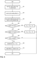
- the controller circuit of the PFC converter may repetitively (e.g. in each PWM switching cycle) perform an algorithm, an example of which is illustrated by the flow chart of Fig. 5 .
- the algorithm may be implemented as an interrupt routine performed by a microcontroller, which may be included in the controller circuit of the PFC converter.
- the current digitized values V IN [ n ] , V OUT [ n ] and i IN [ n ] are obtained from the respective sensor circuits, e.g. from the output registers of respective analog-to-digital converters (see Fig. 5 , step 501).
- the measured current value i IN [ n ] may include a systematic error, which is corrected by adding an offset value ⁇ i OS (see Fig. 5 , step 502).
- the offset value ⁇ i OS may be set to zero.
- the corrected inductor current value is then used to determine the duty cycle D n for the current PWM cycle n (see Fig. 5 , step 503).
- the corrected inductor current value is used as feedback signal input to the control loop that outputs the current duty cycle D n as control variable (wherein the inductor current i IN is the controlled variable).
- step 504 the condition V AC >0 is tested, which results in "yes" during a positive half-wave of the AC input voltage. In this event, the current duty cycle D n is added to D ACC + (step 505).
- step 506 the condition V AC ⁇ 0 is tested, which results in "yes" during a negative half-wave of the AC input voltage. In this event, the current duty cycle D n is added to D ACC ⁇ (step 507).
- the variables D ACC + and D ACC ⁇ may be initialized as zero at the beginning of a period (or the end of the preceding period) of the AC input voltage.
- the end of the current period of the AC input voltage e.g. at the end of the negative half-wave
- a zero-crossing detection e.g. at the end of the negative half-wave
- different approaches to detecting the end of the AC cycle may be used.
- the current offset value ⁇ i OS is modified/adjusted based in the error value E .
- Step 510 may also include the reset of the values D ACC + and D ACC ⁇ to their initial values.
- step 601 the condition E >0 is tested. That is, step 601 yields "yes” if the error value E is positive.
- step 603 the condition E ⁇ 0 is tested. That is, step 603 yields "yes” if the error value E is negative.
- the zero threshold in steps 601 and 603 may be replaced by small finite values.
- the condition tested in step 601 may be E>a (instead of E >0), and the condition tested in step 603 may be E ⁇ -a (instead of E ⁇ 0), wherein a may be a small positive value.
- This approach avoids an adjustment of the offset value ⁇ i OS if the error is small and within the interval [ -a, a ] .
- Fig. 7 illustrates one exemplary embodiment, which includes the totem pole PFC converter circuit of Fig. 3 and a corresponding controller circuit 70, and which is configured to control the switching operation of the PFC converter and to perform the steps illustrated in Figs. 5 and 6 .
- the controller circuit 70 includes, in the present example, a microcontroller 71 as well as the analog-to-digital converters 72, 73, and 74. It is understood that the analog-to-digital converters may be part of the microcontroller's peripheral circuitry and may be integrated in the same semiconductor chip as the microcontroller.
- the analog-to-digital converters may be regarded as sensor circuits (or as parts of sensor circuits) that are configured to repetitively generate measured values of the AC input voltage V AC , the output voltage V OUT and the inductor current i IN .
- the sensor circuit for measuring the inductor current includes a current sensor element CS, which may be, for example, a Hall sensor, wherein the sensor voltage Vcs provided by the sensor element CS represents the inductor current i IN . It is understood that various other concepts for sensing the inductor current may be applicable instead of a Hall sensor.
- transistor cells of transistors T 1 and T 2 may be used to sense the transistor currents when the non-zero transistor current is equal to the inductor current i IN .
- transistors T 1 and T 2 may be used to sense the transistor currents when the non-zero transistor current is equal to the inductor current i IN .
- such concepts are well known in the field of switching converters and thus not further discussed herein.
- the microcontroller 71 may include one or more processors that are configured to execute software instructions stored in a memory (which may also be part of the microcontroller 71).
- the microcontroller 71 may receive a system clock signal from which the PWM cycle period 1/f PWM may be derived.
- the above-mentioned control loop (see Fig. 5 , step 503), which determines the duty cycle D n , may be implemented using the software stored in the memory. Suitable control algorithms are as such known and thus not further discussed herein.
- control loop takes the corrected inductor current value i IN [ n ] as an input, and that the offset value ⁇ i OS , which is used to correct the measured inductor current, is regularly (periodically or from time to time) adjusted as described above with reference to Figs. 5 and 6 .
- Fig. 7 is a simplified example which only includes those components that are relevant to the explanation of the embodiments. Standard components such as voltage regulators, gate driver circuits, etc. have been omitted to keep the focus on the relevant parts. Furthermore, it is emphasized that the method steps illustrated in Fig. 5 and 6 need not necessarily be executed in the depicted order. The skilled person will readily understand that various steps can be rearranged without changing the underlying concept of correcting the DC offset of the measured inductor current based on the duty cycles D n occurring during one AC cycle.
- a totem-pole PFC converter topology is used. As mentioned, this is only an example and other converter topologies may be applicable instead.
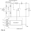
- Fig. 8 illustrates a similar circuit as Fig. 7 , wherein a classical (single-phase) boost PFC converter topology is used instead of the totem-pole PFC converter topology.
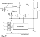
- a dual boost PFC converter topology is used.
- the PCF converter includes a full-bridge rectifier BR and a boost stage.
- the full-bridge rectifier BR is composed of four diodes coupled between the AC voltage source (providing the AC input voltage V AC ) and the boost stage.
- the boost stage is composed of the inductor Li, the electronic switch T 1 (e.g. a MOSFET), the diode D O and the output capacitor C B , which provides the DC output voltage V OUT .
- the controller circuit 70 is basically the same as in the previous example and reference is made to the respective description above. Different to the example of Fig. 7 , only one pulse-width modulated control signal V G1 (gate signal of transistor T 1 ) is needed to control the switching operation of the boost stage.
- the duty cycle values D n may be generated - for each PWM cycle and based on measured values i IN [n] (represents current sense signal V CS ), V IN [n] (represents rectified AC input signal V AC ) and V OUT [n] - in the same way as in the previous example, in which a totem-pole PFC converter topology has been used.
- the first inductor Li, the first transistor T 1 , the first diode D 1 and the output capacitor C B form a first boost converter
- the second inductor L 2 , the second transistor T 2 , the second diode D 2 and the (same) output capacitor C B form a second boost converter
- the first boost converter is only active during the positive half-wave of the AC input voltage V AC and the second boost converter is only active during the negate half-wave.
- the circuit is closed via diode D 3 (in the negative half-wave) and, respectively, via diode D 4 (in die positive half-wave).
- the inductor current i IN may be sensed between the AC voltage source and the common circuit node of inductor Li and diode D 3 . Accordingly, the sensed current values i IN [n] represent the current passing through inductor Li (and diode D 4 ) during the positive half-wave and, respectively, the passing current through inductor L 2 (and diode D 3 ) during the negative half-wave.
- one pulse-width modulated control signal V G1 (gate signal of transistor T 1 ) is needed to control the switching operation of the dual boost stage during the positive half-wave and one pulse-width modulated control signal V G2 (gate signal of transistor T 2 ) is needed to control the switching operation of the dual boost stage during the negative half-wave.
- the duty cycle values D n may be generated - for each PWM cycle and throughout a whole AC cycle and based on measured values i IN [n] (represents current sense signal V CS ), V IN [n] (represents rectified AC input signal V AC ) and V OUT [n] - in the same way as in the first example, in which a totem-pole PFC converter topology has been used.
- One embodiment relates to a method that may be performed by a controller circuit for an AD/DC switching converter. Accordingly, the method includes determining duty cycle values D n for the pulse width modulation (PWM) of one or more switching signals (see, e.g. Figs. 7-9 , gate signal V G1 and, as the case may be, gate signal V G2 ) to operate the AC/DC converter with Power Factor Correction.
- PWM pulse width modulation
- one duty cycle value D n is determined in each PWM cycle based on a measured current value (current feedback loop) that has been corrected using an offset value ⁇ i OS .
- the method further includes accumulating the duty cycle values D n throughout a positive half-wave of an AC input voltage of the AC/DC converter to obtain a first sum value D ACC + and accumulating the duty cycle values D n throughout a negative half-wave of the AC input voltage of the AC/DC converter to obtain a second sum value D ACC ⁇ (cf. Fig. 5 ). Furthermore, the method includes determining an error value E representing the difference between the first sum value and the second sum value and adjusting the offset value ⁇ i OS based on the error value.
- the duty cycle values D n are to be determined such that the inductor current (input current) is at least approximately in phase with the AC input voltage of the AC/DC converter (see, e.g. Fig. 2 ).
- the feedback loop may receive additional input data in addition to the measured inductor current.
- a duty cycle value D n is determined - in each PWM cycle - based on the corrected current value i IN [ n ] , a first measured voltage value V IN [ n ] representing the AC input voltage of the AC/DC converter, and a second measured voltage value V OUT [n] representing the DC output voltage of the AC/DC converter.
- adjusting the offset value ⁇ i OS includes decreasing the offset value ⁇ i OS in the event that the error value is greater than a first threshold ( E > a ) and increasing the offset value ⁇ i OS in the event that the error value is lower than a second threshold ( E ⁇ -a ).
- the first and the second thresholds may be both zero, and the offset value may remain unchanged in the event that the error value is zero or between the thresholds ( -a ⁇ E ⁇ a ) .
- the first and the second sum values are reset to respective initial or reference values in each period of the AC input voltage.
- This initial values may be zero.
- the controller circuit comprises a processor (e.g. the microcontroller 71 as shown in Fig. 7-9 ) and memory (e.g. included in the microcontroller) storing instructions that, when executed by the processor, cause controller circuit to perform the method steps and functions summarized above and depicted, e.g. in Figs. 5 and 6 .
- the processor may use some peripheral circuit components (which may also be included in the microcontroller) such as analog-to-digital converters to perform the desired function.
- a further embodiment relates to a circuit arrangement comprising an AC/DC converter for Power Factor Correction which includes at least one electronic switch and an inductor, and a controller circuit for the AC/DC converter.
- the controller circuit is configured to determine duty cycle values D n for pulse width modulation (PWM) of a switching signal for driving the at least one switch (see, e.g. Figs. 7-9 , gate signal V G1 and, as the case may be, gate signal V G2 ), wherein a duty cycle value is determined in each PWM cycle based on (current feedback loop) a measured inductor current value that has been corrected using an offset value ⁇ i OS .
- PWM pulse width modulation
- the controller circuit is further configured to accumulate the duty cycle values D n throughout a positive half-wave of an AC input voltage of the AC/DC converter to obtain a first sum value D ACC + and to accumulate the duty cycle values throughout a negative half-wave of the AC input voltage of the AC/DC converter to obtain a second sum value D ACC ⁇ (cf. Fig. 5 ). Furthermore, the controller circuit is configured to determine an error value E representing the difference between the first sum value and the second sum value and to adjust the offset value ⁇ i OS based on the error value.
Landscapes
- Engineering & Computer Science (AREA)
- Power Engineering (AREA)
- Rectifiers (AREA)
Priority Applications (1)
| Application Number | Priority Date | Filing Date | Title |
|---|---|---|---|
| EP22199709.1A EP4350966A1 (de) | 2022-10-05 | 2022-10-05 | Schaltwandler mit teilleistungsverarbeitung |
Applications Claiming Priority (1)
| Application Number | Priority Date | Filing Date | Title |
|---|---|---|---|
| EP22199709.1A EP4350966A1 (de) | 2022-10-05 | 2022-10-05 | Schaltwandler mit teilleistungsverarbeitung |
Publications (1)
| Publication Number | Publication Date |
|---|---|
| EP4350966A1 true EP4350966A1 (de) | 2024-04-10 |
Family
ID=83598446
Family Applications (1)
| Application Number | Title | Priority Date | Filing Date |
|---|---|---|---|
| EP22199709.1A Pending EP4350966A1 (de) | 2022-10-05 | 2022-10-05 | Schaltwandler mit teilleistungsverarbeitung |
Country Status (1)
| Country | Link |
|---|---|
| EP (1) | EP4350966A1 (de) |
Citations (8)
| Publication number | Priority date | Publication date | Assignee | Title |
|---|---|---|---|---|
| GB2019141A (en) * | 1978-04-12 | 1979-10-24 | Hitachi Ltd | Drive circuit for magnetic bubble device |
| EP0913027B1 (de) * | 1996-07-16 | 2003-01-22 | Danfoss A/S | Verfahren zum kommutieren eines bürstenlosen motors undstromversorgung für einen bürstenlosen motor |
| US6981185B1 (en) * | 2002-08-09 | 2005-12-27 | Adaptec, Inc. | Methods and apparatus to correct duty cycle |
| EP2197250A1 (de) * | 2007-09-27 | 2010-06-16 | Iwasaki Electric Co., Ltd | Beleuchtungsvorrichtung für eine hochspannungsentladungslampe, beleuchtungsverfahren für eine hochspannungsentladungslampe und projektor |
| CN201611786U (zh) * | 2010-02-08 | 2010-10-20 | 南京国睿新能电子有限公司 | 光伏并网逆变器的并网电流直流分量控制装置 |
| JP5874019B2 (ja) * | 2010-11-24 | 2016-03-01 | パナソニックIpマネジメント株式会社 | 直流電源装置 |
| JP2016123148A (ja) * | 2014-12-24 | 2016-07-07 | 三菱電機株式会社 | スイッチング電源装置 |
| CN108879630A (zh) * | 2018-07-11 | 2018-11-23 | 中车永济电机有限公司 | 机车交直交供电系统的变压器直流偏磁抑制方法 |
-
2022
- 2022-10-05 EP EP22199709.1A patent/EP4350966A1/de active Pending
Patent Citations (8)
| Publication number | Priority date | Publication date | Assignee | Title |
|---|---|---|---|---|
| GB2019141A (en) * | 1978-04-12 | 1979-10-24 | Hitachi Ltd | Drive circuit for magnetic bubble device |
| EP0913027B1 (de) * | 1996-07-16 | 2003-01-22 | Danfoss A/S | Verfahren zum kommutieren eines bürstenlosen motors undstromversorgung für einen bürstenlosen motor |
| US6981185B1 (en) * | 2002-08-09 | 2005-12-27 | Adaptec, Inc. | Methods and apparatus to correct duty cycle |
| EP2197250A1 (de) * | 2007-09-27 | 2010-06-16 | Iwasaki Electric Co., Ltd | Beleuchtungsvorrichtung für eine hochspannungsentladungslampe, beleuchtungsverfahren für eine hochspannungsentladungslampe und projektor |
| CN201611786U (zh) * | 2010-02-08 | 2010-10-20 | 南京国睿新能电子有限公司 | 光伏并网逆变器的并网电流直流分量控制装置 |
| JP5874019B2 (ja) * | 2010-11-24 | 2016-03-01 | パナソニックIpマネジメント株式会社 | 直流電源装置 |
| JP2016123148A (ja) * | 2014-12-24 | 2016-07-07 | 三菱電機株式会社 | スイッチング電源装置 |
| CN108879630A (zh) * | 2018-07-11 | 2018-11-23 | 中车永济电机有限公司 | 机车交直交供电系统的变压器直流偏磁抑制方法 |
Similar Documents
| Publication | Publication Date | Title |
|---|---|---|
| US12057776B2 (en) | Method and apparatus for digital, closed-loop control of CrCM switch-mode power converters | |
| US8670255B2 (en) | Utilization of a multifunctional pin combining voltage sensing and zero current detection to control a switched-mode power converter | |
| EP2506413B1 (de) | Stromwandler mit phasenverschobener Ansteuerung und Steuergerät dafür | |
| US12068672B2 (en) | Control circuit for power converter apparatus provided with PFC circuit operating in current-critical mode | |
| US8564992B2 (en) | Power factor correction device and method with off time prediction for critical mode operation | |
| US9455631B2 (en) | Current estimation for a converter | |
| CN101720526A (zh) | 可减少反馈信号的功率因数校正控制器 | |
| US9837902B2 (en) | Switching power source device, semiconductor device, and AC/DC converter | |
| JP2014508499A (ja) | 非対称電圧相殺技術を使ってlclコンバータを制御する方法および装置 | |
| US5615100A (en) | Resonant inverter | |
| US20130100711A1 (en) | Switching Circuit | |
| US11923756B2 (en) | Control apparatus for power conversion apparatus | |
| CN118614002A (zh) | 用于控制电感器-电感器-电容器(llc)电源转换器的脉冲宽度调制(pwm) | |
| US10666131B2 (en) | Dead-time voltage compensation apparatus and dead-time voltage compensation method | |
| US12237763B2 (en) | Dead time adjusted pulse width modulator | |
| JP5933418B2 (ja) | 電力変換装置 | |
| US20250175089A1 (en) | Resonant power converter circuit with adaptive on-time control and method thereof | |
| AU2020400935B2 (en) | Method for identifying the filter inductor of a grid inverter | |
| JP4167811B2 (ja) | スイッチング電源装置 | |
| JP5940798B2 (ja) | ラッチングリレー制御回路及び電力量計 | |
| Yu et al. | A numerical method for calculating the output spectrum of an H-bridge inverter with dead-time based on switching mode analysis | |
| JP5456578B2 (ja) | 電力変換装置 | |
| US20260039222A1 (en) | Multiphase power converter controller | |
| US20260039196A1 (en) | Multiphase power converter controller | |
| US20230361669A1 (en) | Zero Voltage Switching |
Legal Events
| Date | Code | Title | Description |
|---|---|---|---|
| PUAI | Public reference made under article 153(3) epc to a published international application that has entered the european phase |
Free format text: ORIGINAL CODE: 0009012 |
|
| STAA | Information on the status of an ep patent application or granted ep patent |
Free format text: STATUS: THE APPLICATION HAS BEEN PUBLISHED |
|
| AK | Designated contracting states |
Kind code of ref document: A1 Designated state(s): AL AT BE BG CH CY CZ DE DK EE ES FI FR GB GR HR HU IE IS IT LI LT LU LV MC ME MK MT NL NO PL PT RO RS SE SI SK SM TR |
|
| STAA | Information on the status of an ep patent application or granted ep patent |
Free format text: STATUS: REQUEST FOR EXAMINATION WAS MADE |
|
| 17P | Request for examination filed |
Effective date: 20240614 |
|
| RBV | Designated contracting states (corrected) |
Designated state(s): AL AT BE BG CH CY CZ DE DK EE ES FI FR GB GR HR HU IE IS IT LI LT LU LV MC ME MK MT NL NO PL PT RO RS SE SI SK SM TR |
|
| STAA | Information on the status of an ep patent application or granted ep patent |
Free format text: STATUS: EXAMINATION IS IN PROGRESS |
|
| 17Q | First examination report despatched |
Effective date: 20250730 |