EP4350969A1 - Sammelschienenwärmeableitungsstruktur und wechselrichtervorrichtung - Google Patents
Sammelschienenwärmeableitungsstruktur und wechselrichtervorrichtung Download PDFInfo
- Publication number
- EP4350969A1 EP4350969A1 EP22824856.3A EP22824856A EP4350969A1 EP 4350969 A1 EP4350969 A1 EP 4350969A1 EP 22824856 A EP22824856 A EP 22824856A EP 4350969 A1 EP4350969 A1 EP 4350969A1
- Authority
- EP
- European Patent Office
- Prior art keywords
- bus bar
- heat dissipation
- bus
- heat sink
- bus bars
- Prior art date
- Legal status (The legal status is an assumption and is not a legal conclusion. Google has not performed a legal analysis and makes no representation as to the accuracy of the status listed.)
- Granted
Links
Images


Classifications
-
- H—ELECTRICITY
- H05—ELECTRIC TECHNIQUES NOT OTHERWISE PROVIDED FOR
- H05K—PRINTED CIRCUITS; CASINGS OR CONSTRUCTIONAL DETAILS OF ELECTRIC APPARATUS; MANUFACTURE OF ASSEMBLAGES OF ELECTRICAL COMPONENTS
- H05K7/00—Constructional details common to different types of electric apparatus
- H05K7/20—Modifications to facilitate cooling, ventilating, or heating
- H05K7/2089—Modifications to facilitate cooling, ventilating, or heating for power electronics, e.g. for inverters for controlling motor
- H05K7/209—Heat transfer by conduction from internal heat source to heat radiating structure
-
- H—ELECTRICITY
- H02—GENERATION; CONVERSION OR DISTRIBUTION OF ELECTRIC POWER
- H02M—APPARATUS FOR CONVERSION BETWEEN AC AND AC, BETWEEN AC AND DC, OR BETWEEN DC AND DC, AND FOR USE WITH MAINS OR SIMILAR POWER SUPPLY SYSTEMS; CONVERSION OF DC OR AC INPUT POWER INTO SURGE OUTPUT POWER; CONTROL OR REGULATION THEREOF
- H02M7/00—Conversion of AC power input into DC power output; Conversion of DC power input into AC power output
- H02M7/003—Constructional details, e.g. physical layout, assembly, wiring or busbar connections
-
- H—ELECTRICITY
- H05—ELECTRIC TECHNIQUES NOT OTHERWISE PROVIDED FOR
- H05K—PRINTED CIRCUITS; CASINGS OR CONSTRUCTIONAL DETAILS OF ELECTRIC APPARATUS; MANUFACTURE OF ASSEMBLAGES OF ELECTRICAL COMPONENTS
- H05K7/00—Constructional details common to different types of electric apparatus
- H05K7/20—Modifications to facilitate cooling, ventilating, or heating
- H05K7/2039—Modifications to facilitate cooling, ventilating, or heating characterised by the heat transfer by conduction from the heat generating element to a dissipating body
- H05K7/20436—Inner thermal coupling elements in heat dissipating housings, e.g. protrusions or depressions integrally formed in the housing
- H05K7/20445—Inner thermal coupling elements in heat dissipating housings, e.g. protrusions or depressions integrally formed in the housing the coupling element being an additional piece, e.g. thermal standoff
- H05K7/20472—Sheet interfaces
- H05K7/20481—Sheet interfaces characterised by the material composition exhibiting specific thermal properties
-
- H—ELECTRICITY
- H05—ELECTRIC TECHNIQUES NOT OTHERWISE PROVIDED FOR
- H05K—PRINTED CIRCUITS; CASINGS OR CONSTRUCTIONAL DETAILS OF ELECTRIC APPARATUS; MANUFACTURE OF ASSEMBLAGES OF ELECTRICAL COMPONENTS
- H05K7/00—Constructional details common to different types of electric apparatus
- H05K7/20—Modifications to facilitate cooling, ventilating, or heating
- H05K7/2039—Modifications to facilitate cooling, ventilating, or heating characterised by the heat transfer by conduction from the heat generating element to a dissipating body
- H05K7/20509—Multiple-component heat spreaders; Multi-component heat-conducting support plates; Multi-component non-closed heat-conducting structures
Definitions
- the present invention relates to a bus bar heat dissipation structure to be applied to an inverter device.
- An inverter device is one which converts DC power into AC power to drive a motor and the like.
- a smoothing capacitor for smoothing DC power is mounted on a DC power part of the inverter device.
- the conversion from DC power into AC power is carried out by switching operation of a power semiconductor module such as an IGBT.
- Bus bars (specifically, a bus bar P on the positive electrode side and a bus bar N on the negative electrode side) are usually used for the electrical connection between the smoothing capacitor and the power semiconductor module.
- the bus bar connected to the positive electrode of the smoothing capacitor is arranged along the bus bar connected to the negative electrode of the smoothing capacitor, thereby achieving a reduction in inductance.
- the bus bar P and the bus bar N are integrally molded with resin and it is fixed to, for example, an inverter case with a screw via a collar integrally molded at the same time.
- the DC-power-input bus bars it is necessary to design the cross-sectional area so as to have a current density which satisfies the increasing of the heat resistant temperature and internal air temperature of the resin for the integral molding.
- the DC-power-input bus bars are located between the smoothing capacitor and the power semiconductor module, from the point of view of the space restriction of the structure and the inductance reduction of the smoothing capacitor, it is often difficult to suppress the generation of heat by increasing the cross-sectional areas of the bus bars. It has therefore been required to provide a heat dissipation structure to the DC-power-input bus bars.
- a heat dissipation structure of the DC-power-input bus bars for example, a heat dissipation structure provided to the inverter device disclosed in a patent document 1 can be cited.
- Patent Document 1 Japanese Patent Application Publication No. 2009-21445
- a heat sink having a large area is required at the lower part of the bus bar P and the bus bar N, and it is not preferable to reduce the size of the inverter device.
- the present invention is made in consideration of such a technical problem, and an object of the present invention is to improve the rigidity and the heat dissipation performance of bus bars connected to a smoothing capacitor and a power semiconductor module of an inverter device and to reduce the size of the inverter device.
- the present invention in one aspect thereof, is a bus bar heat dissipation structure including: a pair of bus bars disposed along each other between a smoothing capacitor and a power semiconductor module and connected to the smoothing capacitor and the power semiconductor module; a heat sink disposed between the pair of the bus bars along the pair of the bus bars; insulating members disposed between one of the pair of the bus bars and the heat sink and between the other of the pair of the bus bars and the heat sink; and a case on which the power semiconductor module is mounted, wherein the heat sink includes: a heat dissipation main body part disposed between the pair of the bus bars; and a case-side fixing leg part fastened to the case, at one end side of the heat dissipation main body part.
- the bus bar heat dissipation structure further includes a resin member for integrating the pair of the bus bars with the heat sink.
- the bus bar heat dissipation structure further includes a substrate formed with a fixing hole, wherein the heat sink further includes a substrate-side fixing leg part fastened to the substrate via the fixing hole, at an other end side of the heat dissipation main body part, and wherein a pattern connected to an electronic component mounted on the substrate is provided at a periphery of the fixing hole of the substrate.
- the present invention in one aspect thereof, is an inverter device including the bus bar heat dissipation structure mentioned above.
- the rigidity and the heat dissipation performance of the bus bars connected to the smoothing capacitor and the power semiconductor module of the inverter device can be improved and the size of the inverter device can be reduced.
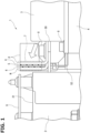
- An inverter device 1 to which a bus bar heat dissipation structure as one embodiment of the present invention shown in FIG. 1 has been applied is provided with a smoothing capacitor 2, a power semiconductor module 3 and a pair of bus bars P and N.
- the power semiconductor module 3 is mounted on a case 4 so as to be parallel to the smoothing capacitor 2, at a position near the smoothing capacitor 2.
- the bus bar P which is one of the bus bars corresponds to a positive electrode bus bar.
- the bus bar N which is the other of the bus bars corresponds to a negative electrode bus bar.
- the bus bars P and N are disposed along each other between the smoothing capacitor 2 and the power semiconductor module 3, and are connected to the smoothing capacitor 2 and the power semiconductor module 3.
- a heat sink 5 is disposed between the bus bars P and N along the bus bars P and N.
- insulating members 6 are disposed between the bus bar P and the heat sink 5 and between the bus bar N and the heat sink 5. Then, the bus bars P and N and the heat sink 5 are integrated with a resin member 7.
- the bus bar P is made of a well-known steel material such as copper and aluminum, and is integrally provided with a bus-bar-P main body part P1, module-side terminal parts P2 and a capacitor-side terminal part P3.
- the bus-bar-P main body part P1 is formed in a rectangular plate shape bent in a crank shape such that the capacitor-side terminal part P3 is arranged parallel to a capacitor-side terminal part N3 of the bus bar N.
- the bus-bar-P main body part P1 is formed with through holes P4 through which projection portions 74 of the resin member 7 locking main body part 71) pass.
- the module-side terminal parts P2 are composed of three (three-phase) terminals which protrude vertically to the bus-bar-P main body part P1 and are fastened to a terminal stand 30 of the power semiconductor module 3 by fixing tools 8 such as screws.
- the capacitor-side terminal part P3 is composed of a single terminal which protrudes toward the direction opposite to the module-side terminal parts P2 on one end side of the bus-bar-P main body part P1 and is fastened to a terminal stand 20 of the smoothing capacitor 2 by a fixing tool 8.
- the bus bar N is made of a well-known steel material such as copper and aluminum, and is provided with a bus-bar-N main body part N1, module-side terminal parts N2 and a capacitor-side terminal part N3.
- the bus-bar-N main body part N1 is formed in a rectangular plate shape which is bent such that the capacitor-side terminal part N3 is arranged parallel to the capacitor-side terminal part P3 of the bus bar P.
- the bus-bar-N main body part N1 is formed with through holes N4 through which the projection portions 74 of the resin member 7 pass.
- the module-side terminal parts N2 are composed of three (three-phase) terminals which protrude vertically to the bus-bar-N main body part N1 and are fastened to the terminal stand 30 of the power semiconductor module 3 by fixing tools 8 so as to be parallel to the respective three module-side terminal parts P2 of the bus bar P.
- the capacitor-side terminal part N3 is composed of a single terminal which protrudes toward the same direction as that of the module-side terminal parts N2 on one end side of the bus-bar-N main body part N1, is arranged parallel to the capacitor-side terminal part P3 of the bus bar P and is fastened to the terminal stand 20 of the smoothing capacitor 2 by a fixing tool 8.
- the heat sink 5 is made of a well-known thermal conductive steel material such as copper steel, iron steel, copper alloy and aluminum alloy, and is provided with a heat dissipation main body part 51 and a case-side fixing leg part 52.
- the heat dissipation main body part 51 is formed in a rectangular plate shape and is disposed between the bus-bar-P main body part P1 and the bus-bar-N main body part N1.
- the heat dissipation main body part 51 is formed with through holes 53 through which the projection portions 74 of the resin member 7 pass.
- the case-side fixing leg part 52 is fastened to the case 4 by a fixing tool 8, on one side of the heat dissipation main body part 51.
- the insulating members 6 are made of a well-known resin material or heat conductive insulating material, are formed in rectangular sheet shapes, and are disposed between the bus bar P and the heat sink 5 and between the bus bar N and the heat sink 5. In addition, the insulating members 6 are each formed with through holes 61 through which the respective projection portions 74 of the resin member 7 pass.
- the resin member 7 is made of heat resistance and insulating resin such as polyphenylene sulfide (PPS) based resin and polybutylene terephthalate (PBT) based resin, and is provided with a locking main body part 71, a bus-bar-P locking part 72 and a capacitor locking part 73.
- PPS polyphenylene sulfide
- PBT polybutylene terephthalate
- the locking main body part 71 is formed in an L-shaped plate shape in cross section so as to come in contact with the bus bar P and to be lockable to the bus bar P, the heat sink 5 and the bus bar N.
- the locking main body part 71 is provided with projection portions 74 which pass through the through holes P4, 61, 53, 61 and N4 of the bus bar P, the insulating member 6, the heat sink 5, the insulating member 6 and the bus bar N.
- the bus-bar-P locking part 72 is formed in a plate shape so as to be lockable to the bus bar P at one end of the locking main body part 71.
- a pair of grooves 75 into which the respective bus-bar-P main body part P1 and bus-bar-N main body part N1 are inserted is provided between the bus-bar-P locking part 72 and the locking main body part 71.
- the capacitor locking part 73 is formed in a plate shape so as to be lockable to the case 4 at a part close to the other end of the locking main body part 71.
- the capacitor locking part 73 is provided with a projection portion 76 to be inserted into an insertion hole 22 in a housing 21 of the smoothing capacitor 2.
- FIGS. 1 to 3 An example of an assembly procedure of the bus bar heat dissipation structure in the present embodiment will be explained while referring to FIGS. 1 to 3 .
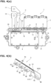
- the insulating members 6 are interposed between the bus bar P and the heat sink 5 and between the bus bar N and the heat sink 5 as shown in FIGS. 1 and 3(a) , and the bus bars P and N, the heat sink 5 and the insulating members 6 are assembled as shown in FIG. 3(b) .
- bus-bar-P main body part P1 and the bus-bar-N main body part N1 are inserted into the grooves 75 of the resin member 7 as shown in FIGS. 3(c) and 3(d) .
- the projection portions 74 of the resin member 7 are inserted into the through holes P4, 61, 53, 61 and N4 of the bus bar P, the insulating member 6, the heat sink 5, the insulating member 6 and the bus bar N.
- the module-side terminal parts P2 and N2 of the bus bars P and N are fastened to the terminal stand 30 of the power semiconductor module 3 by the fixing tools 8.
- the case-side fixing leg part 52 of the heat sink 5 is fastened to the case 4 by the fixing tool 8.
- the capacitor-side terminal parts P3 and N3 of the bus bars P and N are each fastened to the terminal stand 20 of the smoothing capacitor 2 by the fixing tools 8, together with conductors 11 and 12 of FIG. 2 which are connected to a DC power supply part (not shown) of the inverter device 1.
- the bus bars P and N, the heat sink 5 and the insulating members 6 are integrated by the resin member 7.
- the insulating members 6 are formed separately from the resin member 7. Since the resin member 7 has insulation properties, a mode may be used in which the insulating members 6 and the resin member 7 are integrally molded in advance. According to this mode, as compared with the configuration in which the insulating members 6 are formed separately from the resin member 7, the number of assembly processes can be reduced.
- the heat sink 5, the bus bars P and N and the insulating members 6 are integrated, and thereby the heat generated at the bus bars P and N can be dissipated to the case 4 via the heat dissipation main body part 51 and the case-side fixing leg part 52 of the heat sink 5 and the rigidity of the integrated bus bars P and N increases.
- the case-side leg part 52 of the heat sink 5 can be disposed at a part which is a position immediately before current is shunted from the bus bars P and N to the power semiconductor module 3 and at which the current density is the highest.
- the size of the inverter device can be reduced.
- the integrated bus bars P and N can be disposed between electronic components having low noise resistance (after-mentioned substrate 9 and electronic components on the substrate 9) and the power semiconductor module 3. Consequently, the electric field of noises generated from the power semiconductor module 3 toward the direction shown by a white arrow in FIG. 1 is shielded by the bus bars P and N and the magnetic field of the noises is shielded by the heat sink 5, thereby suppressing the occurrence of the malfunction of the electronic components.
- the bus bar heat dissipation structure of the present embodiment the heat dissipation properties and the rigidity of the bus bars P and N connected to the smoothing capacitor 2 and the power semiconductor module 3 of the inverter device 1 are improved and the size of the inverter device 1 can be reduced. In addition, noises from the power semiconductor module 3 to another electronic component can also be shielded.
- the inverter device 1 of FIG. 1 is provided with the substrate 9 on which electronic components such as a CPU for executing, for example, the generation of a switching signal of a semiconductor power module and capacitor are mounted.
- a three-phase DC capacitor hereinafter is referred to as a "Y capacitor" mounted on the substrate 9, there is case where its neutral point grounding (GND connection) is required.
- GND connection neutral point grounding
- the heat sink 5 in the present embodiment shown FIG. 4 is further provided with a substrate-side fixing leg part 54 to be fastened to the substrate 9 and the housing 21 of the smoothing capacitor 2 via a fixing hole formed to the substrate 9, in a mode of the heat sink 5 in the first embodiment.
- the substrate-side fixing leg part 54 is provided in the direction opposite to the case-side fixing leg part 52 at the other end side (substrate 9 side) of the heat dissipation main body part 51, and is fastened to the substrate 9 and the housing 21 of the smoothing capacitor 2 via a fixing hole of the substrate 9 by a conductive fixing tool 8.
- the substrate 9 is provided with patterns to which electronic components such as a CPU and a Y capacitor mounted on the substrate 9 are connected. Moreover, the patterns are also provided to the periphery of the fixing hole (part with which the fixing tool 8 comes in contact).
- the substrate-side fixing leg part 54 that is a part of the heat sink 5 is fastened to the housing 21 of the smoothing capacitor 2 via a fixing hole of the substrate 9, and a grounding terminal of the Y capacitor on the substrate 9 which is positioned near the bus bars P and N is electrically connected to the case 4 via the heat sink 5. Then, the case 4 is grounded, and thereby the grounding of the Y capacitor of the substrate 9 is ensured.
- the bus bar heat dissipation structure of the second embodiment mentioned above in addition to the working effects of the bus bar heat dissipation structure of the first embodiment, the grounding of components inside the substrate 9 can be ensured. In addition, a bus bar and harness for connecting a grounding terminal of a substrate with the case 4 according to conventional technique become unnecessary.
- bus bar heat dissipation structure of the first and second embodiments can also be applied to a bus bar which connects a DC power source (for example, a battery) other than the smoothing capacitor 2 with the power semiconductor module 3.
- a DC power source for example, a battery
Landscapes
- Engineering & Computer Science (AREA)
- Microelectronics & Electronic Packaging (AREA)
- Physics & Mathematics (AREA)
- Thermal Sciences (AREA)
- Power Engineering (AREA)
- Inverter Devices (AREA)
Applications Claiming Priority (2)
| Application Number | Priority Date | Filing Date | Title |
|---|---|---|---|
| JP2021098711A JP7192918B1 (ja) | 2021-06-14 | 2021-06-14 | バスバー放熱構造及びインバータ装置 |
| PCT/JP2022/022866 WO2022264864A1 (ja) | 2021-06-14 | 2022-06-07 | バスバー放熱構造及びインバータ装置 |
Publications (3)
| Publication Number | Publication Date |
|---|---|
| EP4350969A1 true EP4350969A1 (de) | 2024-04-10 |
| EP4350969A4 EP4350969A4 (de) | 2024-08-14 |
| EP4350969B1 EP4350969B1 (de) | 2025-11-26 |
Family
ID=84526415
Family Applications (1)
| Application Number | Title | Priority Date | Filing Date |
|---|---|---|---|
| EP22824856.3A Active EP4350969B1 (de) | 2021-06-14 | 2022-06-07 | Sammelschienenwärmeableitungsstruktur und wechselrichtervorrichtung |
Country Status (5)
| Country | Link |
|---|---|
| US (1) | US12185508B2 (de) |
| EP (1) | EP4350969B1 (de) |
| JP (1) | JP7192918B1 (de) |
| CN (1) | CN117597840B (de) |
| WO (1) | WO2022264864A1 (de) |
Families Citing this family (2)
| Publication number | Priority date | Publication date | Assignee | Title |
|---|---|---|---|---|
| JP2025085151A (ja) * | 2023-11-24 | 2025-06-05 | 三菱電機株式会社 | 電力変換装置 |
| JP2026009726A (ja) * | 2024-07-08 | 2026-01-21 | 株式会社デンソー | 電力変換装置 |
Family Cites Families (18)
| Publication number | Priority date | Publication date | Assignee | Title |
|---|---|---|---|---|
| JP2009021445A (ja) * | 2007-07-12 | 2009-01-29 | Toshiba Corp | インバータ装置 |
| JP5002568B2 (ja) * | 2008-10-29 | 2012-08-15 | 日立オートモティブシステムズ株式会社 | 電力変換装置 |
| JP4935883B2 (ja) * | 2009-11-27 | 2012-05-23 | 株式会社デンソー | バスバーアッセンブリ |
| JP6097557B2 (ja) * | 2012-12-26 | 2017-03-15 | 日立オートモティブシステムズ株式会社 | 電力変換装置 |
| WO2014174767A1 (ja) * | 2013-04-24 | 2014-10-30 | パナソニックIpマネジメント株式会社 | 電力変換装置 |
| JP5714077B2 (ja) * | 2013-10-25 | 2015-05-07 | 三菱電機株式会社 | 接続導体の冷却装置及びそれを用いた電力変換装置 |
| JP6488752B2 (ja) * | 2015-02-19 | 2019-03-27 | 株式会社オートネットワーク技術研究所 | 基板ユニット |
| JP6249992B2 (ja) * | 2015-06-11 | 2017-12-20 | 矢崎総業株式会社 | コネクタモジュールの放熱構造 |
| JP6457895B2 (ja) * | 2015-07-01 | 2019-01-23 | 日立オートモティブシステムズ株式会社 | コンデンサモジュール |
| GB2542353A (en) * | 2015-09-15 | 2017-03-22 | Alstom Technology Ltd | A busbar assembly |
| DE102015224422A1 (de) * | 2015-12-07 | 2017-06-08 | Robert Bosch Gmbh | Elektronische Schaltungseinheit |
| JP2018067998A (ja) * | 2016-10-18 | 2018-04-26 | 三菱電機株式会社 | 電力変換装置 |
| JP7001960B2 (ja) * | 2018-03-23 | 2022-01-20 | 株式会社オートネットワーク技術研究所 | 回路構成体 |
| WO2019208406A1 (ja) * | 2018-04-25 | 2019-10-31 | 株式会社デンソー | 電力変換装置 |
| JP2018166400A (ja) * | 2018-07-18 | 2018-10-25 | 三菱電機株式会社 | 電力変換装置 |
| US10720852B1 (en) * | 2019-01-30 | 2020-07-21 | The United States Of America As Represented By The Secretary Of The Army | High power direct current/alternating current inverter |
| JP2020156206A (ja) * | 2019-03-20 | 2020-09-24 | トヨタ自動車株式会社 | 電力変換器 |
| DE102019218953A1 (de) * | 2019-12-05 | 2021-06-10 | Robert Bosch Gmbh | Elektronische Schaltungseinheit |
-
2021
- 2021-06-14 JP JP2021098711A patent/JP7192918B1/ja active Active
-
2022
- 2022-06-07 US US18/569,967 patent/US12185508B2/en active Active
- 2022-06-07 EP EP22824856.3A patent/EP4350969B1/de active Active
- 2022-06-07 CN CN202280042129.1A patent/CN117597840B/zh active Active
- 2022-06-07 WO PCT/JP2022/022866 patent/WO2022264864A1/ja not_active Ceased
Also Published As
| Publication number | Publication date |
|---|---|
| CN117597840B (zh) | 2024-05-24 |
| EP4350969A4 (de) | 2024-08-14 |
| JP2022191539A (ja) | 2022-12-28 |
| WO2022264864A1 (ja) | 2022-12-22 |
| JP7192918B1 (ja) | 2022-12-20 |
| US20240276684A1 (en) | 2024-08-15 |
| US12185508B2 (en) | 2024-12-31 |
| CN117597840A (zh) | 2024-02-23 |
| EP4350969B1 (de) | 2025-11-26 |
Similar Documents
| Publication | Publication Date | Title |
|---|---|---|
| CN105580263B (zh) | 电力转换装置 | |
| CN104620377B (zh) | 半导体装置 | |
| EP4350969A1 (de) | Sammelschienenwärmeableitungsstruktur und wechselrichtervorrichtung | |
| US11011996B2 (en) | Power converter | |
| EP2579306A2 (de) | Federklemmvorrichtung zur Befestigung eines Leistungshalbleiters | |
| EP3525335B1 (de) | Kondensatoreinheit und elektrischer verdichter | |
| CN115224955A (zh) | 功率转换装置 | |
| CN110168902A (zh) | 电力转换装置 | |
| CN113826315B (zh) | 电力转换装置 | |
| JP2010104146A (ja) | 電力変換装置 | |
| JP7852415B2 (ja) | 電力変換装置 | |
| JP5227259B2 (ja) | 車載用半導体装置 | |
| CN210405842U (zh) | 控制器 | |
| JP7627561B2 (ja) | 電子装置 | |
| CN112951818B (zh) | 功率转换装置 | |
| JP7046146B1 (ja) | 電力変換装置 | |
| EP4503881A1 (de) | Elektrische vorrichtung, verfahren zur montage der elektrischen vorrichtung und fahrzeug mit der elektrischen vorrichtung | |
| CN121013302A (zh) | 用于容纳和冷却电气构件的构件载体 | |
| WO2020201799A1 (ja) | 電力変換装置 | |
| CN118633232A (zh) | 电力转换装置 | |
| CN121192469A (zh) | 汇流条以及电源装置 | |
| JP2025134610A (ja) | 電力変換装置 | |
| JP2025177080A (ja) | 電力変換装置 | |
| JP2023080456A (ja) | 電流センサ及びそれを用いた電力変換装置 | |
| JP5754419B2 (ja) | 半導体装置 |
Legal Events
| Date | Code | Title | Description |
|---|---|---|---|
| STAA | Information on the status of an ep patent application or granted ep patent |
Free format text: STATUS: THE INTERNATIONAL PUBLICATION HAS BEEN MADE |
|
| PUAI | Public reference made under article 153(3) epc to a published international application that has entered the european phase |
Free format text: ORIGINAL CODE: 0009012 |
|
| STAA | Information on the status of an ep patent application or granted ep patent |
Free format text: STATUS: REQUEST FOR EXAMINATION WAS MADE |
|
| 17P | Request for examination filed |
Effective date: 20240103 |
|
| AK | Designated contracting states |
Kind code of ref document: A1 Designated state(s): AL AT BE BG CH CY CZ DE DK EE ES FI FR GB GR HR HU IE IS IT LI LT LU LV MC MK MT NL NO PL PT RO RS SE SI SK SM TR |
|
| A4 | Supplementary search report drawn up and despatched |
Effective date: 20240717 |
|
| RIC1 | Information provided on ipc code assigned before grant |
Ipc: H05K 7/20 20060101ALI20240711BHEP Ipc: H02M 7/48 20070101AFI20240711BHEP |
|
| DAV | Request for validation of the european patent (deleted) | ||
| DAX | Request for extension of the european patent (deleted) | ||
| REG | Reference to a national code |
Ref country code: DE Free format text: PREVIOUS MAIN CLASS: H02M0007480000 Ipc: H05K0007200000 Ref country code: DE Ref legal event code: R079 Ref document number: 602022025792 Country of ref document: DE Free format text: PREVIOUS MAIN CLASS: H02M0007480000 Ipc: H05K0007200000 |
|
| RIC1 | Information provided on ipc code assigned before grant |
Ipc: H02M 7/00 20060101ALI20250207BHEP Ipc: H05K 7/20 20060101AFI20250207BHEP |
|
| GRAP | Despatch of communication of intention to grant a patent |
Free format text: ORIGINAL CODE: EPIDOSNIGR1 |
|
| STAA | Information on the status of an ep patent application or granted ep patent |
Free format text: STATUS: GRANT OF PATENT IS INTENDED |
|
| INTG | Intention to grant announced |
Effective date: 20250717 |
|
| GRAS | Grant fee paid |
Free format text: ORIGINAL CODE: EPIDOSNIGR3 |
|
| GRAA | (expected) grant |
Free format text: ORIGINAL CODE: 0009210 |
|
| STAA | Information on the status of an ep patent application or granted ep patent |
Free format text: STATUS: THE PATENT HAS BEEN GRANTED |
|
| AK | Designated contracting states |
Kind code of ref document: B1 Designated state(s): AL AT BE BG CH CY CZ DE DK EE ES FI FR GB GR HR HU IE IS IT LI LT LU LV MC MK MT NL NO PL PT RO RS SE SI SK SM TR |
|
| REG | Reference to a national code |
Ref country code: CH Ref legal event code: F10 Free format text: ST27 STATUS EVENT CODE: U-0-0-F10-F00 (AS PROVIDED BY THE NATIONAL OFFICE) Effective date: 20251126 Ref country code: GB Ref legal event code: FG4D |
|
| REG | Reference to a national code |
Ref country code: IE Ref legal event code: FG4D |
|
| REG | Reference to a national code |
Ref country code: DE Ref legal event code: R096 Ref document number: 602022025792 Country of ref document: DE |
|
| REG | Reference to a national code |
Ref country code: NL Ref legal event code: MP Effective date: 20251126 |
|
| PG25 | Lapsed in a contracting state [announced via postgrant information from national office to epo] |
Ref country code: ES Free format text: LAPSE BECAUSE OF FAILURE TO SUBMIT A TRANSLATION OF THE DESCRIPTION OR TO PAY THE FEE WITHIN THE PRESCRIBED TIME-LIMIT Effective date: 20251126 |
|
| REG | Reference to a national code |
Ref country code: LT Ref legal event code: MG9D |
|
| PG25 | Lapsed in a contracting state [announced via postgrant information from national office to epo] |
Ref country code: NO Free format text: LAPSE BECAUSE OF FAILURE TO SUBMIT A TRANSLATION OF THE DESCRIPTION OR TO PAY THE FEE WITHIN THE PRESCRIBED TIME-LIMIT Effective date: 20260226 |
|
| PG25 | Lapsed in a contracting state [announced via postgrant information from national office to epo] |
Ref country code: FI Free format text: LAPSE BECAUSE OF FAILURE TO SUBMIT A TRANSLATION OF THE DESCRIPTION OR TO PAY THE FEE WITHIN THE PRESCRIBED TIME-LIMIT Effective date: 20251126 Ref country code: HR Free format text: LAPSE BECAUSE OF FAILURE TO SUBMIT A TRANSLATION OF THE DESCRIPTION OR TO PAY THE FEE WITHIN THE PRESCRIBED TIME-LIMIT Effective date: 20251126 Ref country code: AT Free format text: LAPSE BECAUSE OF FAILURE TO SUBMIT A TRANSLATION OF THE DESCRIPTION OR TO PAY THE FEE WITHIN THE PRESCRIBED TIME-LIMIT Effective date: 20251126 |
|
| REG | Reference to a national code |
Ref country code: AT Ref legal event code: MK05 Ref document number: 1862522 Country of ref document: AT Kind code of ref document: T Effective date: 20251126 |
|
| PG25 | Lapsed in a contracting state [announced via postgrant information from national office to epo] |
Ref country code: NL Free format text: LAPSE BECAUSE OF FAILURE TO SUBMIT A TRANSLATION OF THE DESCRIPTION OR TO PAY THE FEE WITHIN THE PRESCRIBED TIME-LIMIT Effective date: 20251126 |
|
| PG25 | Lapsed in a contracting state [announced via postgrant information from national office to epo] |
Ref country code: RS Free format text: LAPSE BECAUSE OF FAILURE TO SUBMIT A TRANSLATION OF THE DESCRIPTION OR TO PAY THE FEE WITHIN THE PRESCRIBED TIME-LIMIT Effective date: 20260226 |
|
| PG25 | Lapsed in a contracting state [announced via postgrant information from national office to epo] |
Ref country code: IS Free format text: LAPSE BECAUSE OF FAILURE TO SUBMIT A TRANSLATION OF THE DESCRIPTION OR TO PAY THE FEE WITHIN THE PRESCRIBED TIME-LIMIT Effective date: 20260326 |
|
| PG25 | Lapsed in a contracting state [announced via postgrant information from national office to epo] |
Ref country code: PT Free format text: LAPSE BECAUSE OF FAILURE TO SUBMIT A TRANSLATION OF THE DESCRIPTION OR TO PAY THE FEE WITHIN THE PRESCRIBED TIME-LIMIT Effective date: 20260326 |
|
| PG25 | Lapsed in a contracting state [announced via postgrant information from national office to epo] |
Ref country code: PL Free format text: LAPSE BECAUSE OF FAILURE TO SUBMIT A TRANSLATION OF THE DESCRIPTION OR TO PAY THE FEE WITHIN THE PRESCRIBED TIME-LIMIT Effective date: 20251126 |
|
| PG25 | Lapsed in a contracting state [announced via postgrant information from national office to epo] |
Ref country code: LV Free format text: LAPSE BECAUSE OF FAILURE TO SUBMIT A TRANSLATION OF THE DESCRIPTION OR TO PAY THE FEE WITHIN THE PRESCRIBED TIME-LIMIT Effective date: 20251126 |