EP4351024A1 - Hf-kommunikationsvorrichtung und betriebsverfahren - Google Patents
Hf-kommunikationsvorrichtung und betriebsverfahren Download PDFInfo
- Publication number
- EP4351024A1 EP4351024A1 EP22306501.2A EP22306501A EP4351024A1 EP 4351024 A1 EP4351024 A1 EP 4351024A1 EP 22306501 A EP22306501 A EP 22306501A EP 4351024 A1 EP4351024 A1 EP 4351024A1
- Authority
- EP
- European Patent Office
- Prior art keywords
- communication device
- phase
- phases
- radio frequency
- frequency signal
- Prior art date
- Legal status (The legal status is an assumption and is not a legal conclusion. Google has not performed a legal analysis and makes no representation as to the accuracy of the status listed.)
- Pending
Links
- 238000004891 communication Methods 0.000 title claims abstract description 84
- 238000011017 operating method Methods 0.000 title 1
- 238000005259 measurement Methods 0.000 claims abstract description 45
- 238000000034 method Methods 0.000 claims abstract description 18
- 238000012545 processing Methods 0.000 claims description 16
- 238000011084 recovery Methods 0.000 claims description 6
- 238000001514 detection method Methods 0.000 claims description 5
- 230000010363 phase shift Effects 0.000 claims description 5
- 238000004519 manufacturing process Methods 0.000 description 6
- 230000006735 deficit Effects 0.000 description 3
- 238000013461 design Methods 0.000 description 3
- 238000011161 development Methods 0.000 description 2
- 238000012163 sequencing technique Methods 0.000 description 2
- 238000012360 testing method Methods 0.000 description 2
- 238000012935 Averaging Methods 0.000 description 1
- 238000004364 calculation method Methods 0.000 description 1
- 238000012790 confirmation Methods 0.000 description 1
- 239000013078 crystal Substances 0.000 description 1
- 230000001419 dependent effect Effects 0.000 description 1
- 238000005516 engineering process Methods 0.000 description 1
- 238000001914 filtration Methods 0.000 description 1
- 238000012805 post-processing Methods 0.000 description 1
- 238000005070 sampling Methods 0.000 description 1
- 230000001360 synchronised effect Effects 0.000 description 1
Images





Classifications
-
- H—ELECTRICITY
- H04—ELECTRIC COMMUNICATION TECHNIQUE
- H04L—TRANSMISSION OF DIGITAL INFORMATION, e.g. TELEGRAPHIC COMMUNICATION
- H04L27/00—Modulated-carrier systems
- H04L27/32—Carrier systems characterised by combinations of two or more of the types covered by groups H04L27/02, H04L27/10, H04L27/18 or H04L27/26
- H04L27/34—Amplitude- and phase-modulated carrier systems, e.g. quadrature-amplitude modulated carrier systems
- H04L27/36—Modulator circuits; Transmitter circuits
- H04L27/362—Modulation using more than one carrier, e.g. with quadrature carriers, separately amplitude modulated
- H04L27/364—Arrangements for overcoming imperfections in the modulator, e.g. quadrature error or unbalanced I and Q levels
-
- H—ELECTRICITY
- H04—ELECTRIC COMMUNICATION TECHNIQUE
- H04B—TRANSMISSION
- H04B5/00—Near-field transmission systems, e.g. inductive or capacitive transmission systems
- H04B5/70—Near-field transmission systems, e.g. inductive or capacitive transmission systems specially adapted for specific purposes
-
- H—ELECTRICITY
- H04—ELECTRIC COMMUNICATION TECHNIQUE
- H04W—WIRELESS COMMUNICATION NETWORKS
- H04W4/00—Services specially adapted for wireless communication networks; Facilities therefor
- H04W4/80—Services using short range communication, e.g. near-field communication [NFC], radio-frequency identification [RFID] or low energy communication
-
- H—ELECTRICITY
- H04—ELECTRIC COMMUNICATION TECHNIQUE
- H04B—TRANSMISSION
- H04B1/00—Details of transmission systems, not covered by a single one of groups H04B3/00 - H04B13/00; Details of transmission systems not characterised by the medium used for transmission
- H04B1/02—Transmitters
- H04B1/04—Circuits
- H04B1/0475—Circuits with means for limiting noise, interference or distortion
-
- H—ELECTRICITY
- H04—ELECTRIC COMMUNICATION TECHNIQUE
- H04B—TRANSMISSION
- H04B5/00—Near-field transmission systems, e.g. inductive or capacitive transmission systems
- H04B5/40—Near-field transmission systems, e.g. inductive or capacitive transmission systems characterised by components specially adapted for near-field transmission
- H04B5/48—Transceivers
Definitions
- the present disclosure relates to a radio frequency (RF) communication device. Furthermore, the present disclosure relates to a corresponding method of operating an RF communication device.
- RF radio frequency
- RF communication devices such as radio frequency identification (RFID) devices and near field communication (NFC) devices
- RFID transponders are widely used, in different areas of industry and commerce and for various purposes.
- RFID transponders may for example be embodied as so-called RFID tags or RFID cards.
- RFID tags may be embodied as so-called RFID tags or RFID cards.
- NFC near field communication
- the principles disclosed herein may also be applied to NFC transponders.
- NFC refers to a set of communication protocols that enable two electronic devices to establish communication by bringing them within proximity of each other.
- NFC The communication range of NFC is typically in the order of centimeters (e.g., 10 centimeters or less).
- NFC technology can be used to carry out various transactions, such as transactions for accessing buildings, transactions for accessing public transportation sites or vehicles, and payment transactions.
- a radio frequency (RF) communication device comprising: a receiver unit configured to receive at least one radio frequency signal, wherein the receiver unit has a variable initial phase; a controller configured to change said initial phase; a measurement unit configured to measure a plurality of amplitudes and/or phases of the radio frequency signal, wherein each of said amplitudes and/or phases of the radio frequency signal corresponds to a different initial phase of the receiver unit.
- RF radio frequency
- the controller is configured to rotate the initial phase of the receiver unit in order to obtain a plurality of different initial phases.
- the controller is configured to rotate the initial phase along an IQ-plane, such that the different initial phases are equidistant phase locations along the IQ-plane.
- the controller is configured to rotate the initial phase of the receiver unit across a full trigonometric circle or across a part of said trigonometric circle.
- the RF communication device further comprises a processing unit configured to calculate an average value of the plurality of measured amplitudes and/or phases of the radio frequency signal.
- the processing unit is configured to calculate the average of the measured phases after adding a receiver clock phase shift for each of the measured phases.
- the RF communication device further comprises a clock recovery unit configured to lock a mixer clock of the receiver unit to the phase of the radio frequency signal.
- the RF communication device further comprises a transmitter unit and a reference clock, wherein the reference clock is shared between the receiver unit and the transmitter unit, and wherein the controller is further configured to change an initial phase of the transmitter unit.
- the measurement unit is configured to measure a plurality of further amplitudes and/or phases of the radio frequency signal, wherein each of said further amplitudes and/or phases of the radio frequency signal corresponds to a different initial phase of the transmitter unit.
- the RF communication device further comprises a processing unit configured to calculate an average value of the plurality of measured further amplitudes and/or phases of the radio frequency signal.
- the RF communication device is a near field communication (NFC) device and/or a wireless charging device.
- NFC near field communication
- the RF communication device is configured to perform a low-power card detection for NFC or NFC-based wireless charging.
- a method of operating a radio frequency (RF) communication device comprising a receiver unit, a controller and a measurement unit, and the method comprising: receiving, by the receiver unit, at least one radio frequency signal, wherein the receiver unit has a variable initial phase; changing, by the controller, said initial phase; measuring, by the measurement unit, a plurality of amplitudes and/or phases of the radio frequency signal, wherein each of said amplitudes and/or phases of the radio frequency signal corresponds to a different initial phase of the receiver unit.
- RF radio frequency
- RF communication devices such as radio frequency identification (RFID) devices and near field communication (NFC) devices
- RFID radio frequency identification
- NFC near field communication
- RSSI received signal strength indicator
- IC integrated circuit
- amplitude/gain calibrations during chip manufacturing amplitude/gain calibrations during chip manufacturing
- customer manufacturing tests involving calibration of platform non-idealities (antenna, matching network, etc.).
- a typical target for the accuracy may be to keep the error margin as small as a few percent.
- Accurate phase measurements are useful in various systems and applications, such as clock recovery systems and phase calibrations during chip manufacturing, and customer manufacturing tests (matching network phase calibration), especially in RFID/NFC systems. Furthermore, simultaneous amplitude and phase measurements are also a useful feature in, at least, the use cases of low-power card detection (LPCD) in NFC-based transactions between devices and in NFC-based wireless charging devices.
- LPCD low-power card detection
- a reader When there is card in proximity, the characteristics of the feedback signal to the input terminal of the receiver unit within the reader changes, in particular the amplitude and/or phase of the feedback signal. The ability to measure this change of the characteristics is a key performance indicator. Similar to LPCD for use in NFC-based transactions, accurate phase measurements are useful for LPCD in NFC-based wireless charging devices. In these devices, the input signal may be highly distorted.
- Amplitude and phase measurement units typically use the main receiver path of an RF communication device. Therefore, only a limited amount of additional hardware is needed to perform this function, or no additional hardware at all.
- the amplitude and phase measurement may involve calibration of the RF/analog front-end.
- the accuracy of the amplitude and phase measurement accuracy is limited by IQ mismatch, i.e., the mismatch between offsets, gains and phases in the I-channel and the Q-channel of the receiver unit. Given such remaining IQ imbalances and/or strong distortion, i.e., harmonic content, of the input signal, it may be difficult to realize an accurate amplitude/RSSI and phase measurement unit.
- the RF communication device may be implemented as an RFID device, more specifically as an NFC device.
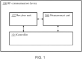
- Fig. 1 shows an illustrative embodiment of an RF communication device 100.
- the RF communication device 100 comprises a receiver unit 102, a controller 104 and a measurement unit 106.
- the receiver unit 102 is configured to receive at least one radio frequency signal, wherein the receiver unit has a variable initial phase.
- the controller 104 is configured to change said initial phase.
- the measurement unit 106 is configured to measure a plurality of amplitudes and/or phases of the radio frequency signal, wherein each of said amplitudes and/or phases of the radio frequency signal corresponds to a different initial phase of the receiver unit.
- the initial phase of the receiver may specifically refer to a clock offset applied to a mixer comprised in the receiver.
- the initial phase may refer to a clock offset applied to other components of the receiver, such as a baseband amplifier (BBA) or baseband processor and an analog-to-digital converter (ADC).
- BBA baseband amplifier
- ADC analog-to-digital converter
- the initial phase of the receiver may correspond to the initial phase of the mixer clock, which can be shifted by a clock generator.
- the clocks of the following blocks in the receiver i.e., BBA and ADC
- the initial phase refers to a signal processed by the receiver unit, in particular to the clock signal provided to the mixer and optionally to other components of the receiver unit.
- a variable initial phase means that the initial phase is adjustable, or in other words that the clock offset applied to the mixer and the other components can be adjusted.
- the controller is configured to rotate the initial phase of the receiver unit in order to obtain a plurality of different initial phases. Thereby, it may be achieved that a suitable set of initial phases is selected, which may be combined to increase the accuracy of the measurement of the amplitude and/or phase of a received RF signal. Furthermore, in one or more embodiments, the controller is configured to rotate the initial phase along an IQ-plane, such that the different initial phases are equidistant phase locations along the IQ-plane. Thereby, a particularly suitable set of initial phases is obtained, which may be combined to increase the measurement accuracy. In a practical implementation, the controller is configured to rotate the initial phase of the receiver unit across a full trigonometric circle or across a part of said trigonometric circle.
- the RF communication device further comprises a processing unit configured to calculate an average value of the plurality of measured amplitudes and/or phases of the radio frequency signal.
- the processing unit may be a stand-alone unit within the RF communication device or be integrated into the measurement unit, for example.
- the processing unit is configured to calculate the average of the measured phases after adding a receiver clock phase shift for each of the measured phases. Thereby, an accurate phase value may be produced, based on the combination of the measured phases at different initial phases of the receiver unit.
- the RF communication device further comprises a clock recovery unit configured to lock a mixer clock of the receiver unit to the phase of the radio frequency signal.
- the receiver unit may be phase-and-frequency locked on the input signal.
- the RF communication device further comprises a transmitter unit and a reference clock, wherein the reference clock is shared between the receiver unit and the transmitter unit, and wherein the controller is further configured to change an initial phase of the transmitter unit.
- the measurement unit may be configured to measure a plurality of further amplitudes and/or phases of the radio frequency signal, wherein each of said further amplitudes and/or phases of the radio frequency signal corresponds to a different initial phase of the transmitter unit.
- the RF communication device may further comprise a processing unit configured to calculate an average value of the plurality of measured further amplitudes and/or phases of the radio frequency signal.
- a variable phase shift may be applied to the transmitter unit of the RF communication device, for example to properly calibrate an off-chip element, such as a matching network.
- the RF communication device may be implemented as a near field communication (NFC) device and/or a wireless charging device.
- the RF communication device may be configured to perform a low-power card detection for NFC or NFC-based wireless charging. Both the low-power card detection and the wireless charging may require an accurate estimation of the amplitude and/or phase of the received signal.
- Fig. 2 shows an illustrative embodiment of a method 200 of operating an RF communication device.
- the method 200 comprises the following steps.
- a receiver unit comprised in the RF communication device receives at least one radio frequency signal, wherein the receiver unit has a variable initial phase.
- a controller comprised in the RF communication device changes said initial phase.
- a measurement unit comprised in the RF communication device measures a plurality of amplitudes and/or phases of the radio frequency signal, wherein each of said amplitudes and/or phases of the radio frequency signal corresponds to a different initial phase of the receiver unit.
- a more accurate estimation of the amplitude and/or phase of the received signal may be achieved.
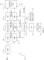
- Fig. 3 shows another illustrative embodiment of an RF communication device 300.
- a possible implementation is shown of an RF communication device according to the present disclosure.
- the skilled person will appreciate that the presently disclosed RF communication device may also be implemented in a different manner, with less or more components than the RF communication device 300 shown in Fig. 3 .
- the RF communication device 300 comprises an RF front-end (RFFE) 302 couped to an I-channel and a Q-channel receiver path.
- the I-channel receiver path comprises a mixer 302, a baseband amplifier 306, and an analog-to-digital converter 308.
- the Q-channel receiver path comprises a mixer 310, a baseband amplifier 312, and an analog-to-digital converter 314.
- the RF communication device comprises an amplitude and phase measurement unit 316, i.e., a measurement unit of the kind set forth above.
- the RF communication device 300 comprises a clock generator 318, a phase-locked loop 320, an XTAL/reference clock 322, and a finite state machine 324 for controlling the amplitude and/or phase measurement.
- the receiver system shown in Fig. 3 includes a crystal (XTAL) 322 functioning as a reference clock, a phase-locked loop (PLL) 320, and a clock generator 318 which provides all required clocks to the receiver.
- XTAL crystal
- PLL phase-locked loop
- Fig. 3 shows a possible implementation of an RF communication device according to the present disclosure. In other possible implementations, the receiver might use a carrier recovery loop to operate without any XTAL or external clock.
- the receiver includes an RF front-end (RFFE) 302, mixers 304, 310 (either continuous-time or discrete-time/ sampling mixers), baseband processing units 306, 312 which might include some gain (fixed or variable, continuous or discrete-time) and some filtering (continuous or discrete-time), analog-to-digital converters (ADCs) 308, 314, an amplitude-and/or-phase measurement unit 316, and a finite state machine 324 that controls the amplitude and/or phase measurement.
- the initial phase of the receiver may correspond to the initial phase of the mixer clock (i.e., clk_mix_i and clk_mix_q in Fig.
- the initial phase of the receiver may correspond to the initial phase of the baseband processing units 306, 312 (i.e., clk_bba_i and clk_bba_q) and the initial phase of the ADCs 308, 314 (i.e., clk_adc_i and clk_adc_q).
- changing or rotating the initial phase of the receiver means that the clocks provided to the mixers 304, 310, and optionally the clocks provided to the baseband processing units 306, 312 and ADCs 308, 314, are varied in steps.
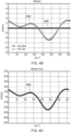
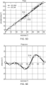
- Figs. 4A to 4E show a real IQ constellation 400 and an ideal IQ constellation 402, a real modulus 404 and an ideal modulus 406, a modulus error 408, a real phase 410 and an ideal phase 412, and a phase error 414, respectively.
- Ioff represents the DC offset on the I-path
- Qoff represents the offset on the Q-path.
- the amplitude measurement error may be as large as 25% and the phase error as large as 14°, depending on the initial phase of the receiver unit.
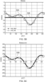
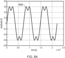
- Figs. 6A to 6C show an input signal 600 of the RF communication device, a measured amplitude 602 and an averaged amplitude 604 of the input signal, and a measured phase 606 and an averaged phase 608 of the input signal, respectively. More specifically, it is shown that by applying one or more of the principles disclosed herein a significant error reduction may also be achieved with a highly distorted input signal. It is noted that the same IQ impairments (offset error, gain error, phase error) as shown in Figs. 5A to 5F apply in this scenario as well. In particular, it may be observed that a significant error reduction in the amplitude and phase measurements may be achieved by a computation at 16 different angles.
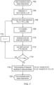
- Fig. 7 shows another illustrative embodiment of a method 700 of operating an RF communication device.
- the method 700 comprises the following steps.
- the amplitude and/or phase measurement is started.
- an initialization step is performed.
- the clock phase of the mixer comprised in the receiver unit is adjusted.
- the clock phase of other components such as a baseband processing unit and analog-to-digital converter, may be adjusted.
- I and Q samples are acquired, at 710, the corresponding amplitude and phase are calculated, and at 712, the results are stored in a table before further processing.
- Fig. 7 shows a suitable sequencing which allows rotating across the trigonometric circle, and which significantly reduces the amplitude and phase errors caused by IQ impairments.
- the initial phase shift of the receiver unit is adjusted in order to implement this phase rotation, which facilitates increasing the accuracy of amplitude and phase measurements. It is noted that the gain settings of the receiver unit may be frozen during this sequencing.
- the principles disclosed herein are not limited to a specific algorithm for calculating the amplitude and phase.
- any suitable algorithm may be used for combined the measured amplitudes and/or phases obtained for the different initial phases of the receiver unit.
- a Cordic algorithm may be used for iteratively calculating the amplitude and phase.
- the angle may be calculated offline by a CPU using any suitable arc-tangent function means (e.g., LUT, atan, atan2).
- time-averaging may be applied to reduce the impact of noise.
- the receiver unit may include a clock recovery system in order to be phase-and-frequency locked on the input RF signal.
- the receiver unit may be synchronized to a transmitter unit included in the same chip.
- an external matching network or filter may be calibrated by applying one or more of the principles disclosed herein.
- the phase rotation may be performed across the full trigonometric circle, or across a part of the trigonometric circle (e.g., 1, 2 or 3 quadrants).
Landscapes
- Engineering & Computer Science (AREA)
- Computer Networks & Wireless Communication (AREA)
- Signal Processing (AREA)
- Circuits Of Receivers In General (AREA)
Priority Applications (3)
| Application Number | Priority Date | Filing Date | Title |
|---|---|---|---|
| EP22306501.2A EP4351024A1 (de) | 2022-10-06 | 2022-10-06 | Hf-kommunikationsvorrichtung und betriebsverfahren |
| US18/469,164 US12348353B2 (en) | 2022-10-06 | 2023-09-18 | RF communication device and operating method |
| CN202311252197.3A CN117858054A (zh) | 2022-10-06 | 2023-09-26 | Rf通信装置和操作方法 |
Applications Claiming Priority (1)
| Application Number | Priority Date | Filing Date | Title |
|---|---|---|---|
| EP22306501.2A EP4351024A1 (de) | 2022-10-06 | 2022-10-06 | Hf-kommunikationsvorrichtung und betriebsverfahren |
Publications (1)
| Publication Number | Publication Date |
|---|---|
| EP4351024A1 true EP4351024A1 (de) | 2024-04-10 |
Family
ID=83902791
Family Applications (1)
| Application Number | Title | Priority Date | Filing Date |
|---|---|---|---|
| EP22306501.2A Pending EP4351024A1 (de) | 2022-10-06 | 2022-10-06 | Hf-kommunikationsvorrichtung und betriebsverfahren |
Country Status (3)
| Country | Link |
|---|---|
| US (1) | US12348353B2 (de) |
| EP (1) | EP4351024A1 (de) |
| CN (1) | CN117858054A (de) |
Citations (2)
| Publication number | Priority date | Publication date | Assignee | Title |
|---|---|---|---|---|
| US20050270095A1 (en) * | 2004-06-04 | 2005-12-08 | Andrew Corporation, A Delaware Corporation | Paralleling digital-input amplifiers |
| US20150229417A1 (en) * | 2014-02-10 | 2015-08-13 | Spirent Communications, Inc. | Automatic phase calibration |
Family Cites Families (17)
| Publication number | Priority date | Publication date | Assignee | Title |
|---|---|---|---|---|
| DE1129180B (de) * | 1961-03-30 | 1962-05-10 | Telefunken Patent | Empfangseinrichtung fuer Impulsuebertragung durch quantisierte Phasenmodulation eines Traegers |
| US5677934A (en) * | 1992-12-30 | 1997-10-14 | Nokia Mobile Phones Limited | Multipath propagation compensation in a TDMA system |
| US5497400A (en) * | 1993-12-06 | 1996-03-05 | Motorola, Inc. | Decision feedback demodulator with phase and frequency estimation |
| US5537121A (en) * | 1995-04-28 | 1996-07-16 | Trimble Navigation Limited | Carrier phase multipath reduction technique |
| US6134282A (en) * | 1997-06-18 | 2000-10-17 | Lsi Logic Corporation | Method for lowpass filter calibration in a satellite receiver |
| US20060074558A1 (en) * | 2003-11-26 | 2006-04-06 | Williamson Walton R | Fault-tolerant system, apparatus and method |
| JP4381945B2 (ja) * | 2004-09-30 | 2009-12-09 | 株式会社ルネサステクノロジ | 受信機、受信方法及び携帯無線端末 |
| JP2006261714A (ja) * | 2005-03-15 | 2006-09-28 | Renesas Technology Corp | 通信用半導体集積回路および携帯通信端末 |
| US7643600B2 (en) * | 2006-11-30 | 2010-01-05 | Silicon Laboratories, Inc. | Techniques for performing gain and phase correction in a complex radio frequency receiver |
| US8064863B1 (en) * | 2008-02-14 | 2011-11-22 | Rf Micro Devices, Inc. | Image rejection calibration |
| FR2932344B1 (fr) * | 2008-06-06 | 2010-06-04 | Thales Sa | Procede de poursuite de la phase d'un signal module par modulation a phase continue et dispositif de synchronisation mettant en oeuvre le procede. |
| US9634878B1 (en) * | 2011-09-08 | 2017-04-25 | See Scan, Inc. | Systems and methods for data transfer using self-synchronizing quadrature amplitude modulation (QAM) |
| US8600319B2 (en) * | 2011-10-14 | 2013-12-03 | Intel Mobile Communications GmbH | Feedback receiver for antenna tuner calculations |
| US8909150B2 (en) * | 2012-03-14 | 2014-12-09 | Nokia Corporation | Method, apparatus, and computer program product for short-range wireless communication |
| US9806771B1 (en) | 2016-08-01 | 2017-10-31 | Nxp B.V. | Method and system for high resolution tuning of the phase for active load modulation in a NFC system |
| US20180275281A1 (en) * | 2017-03-24 | 2018-09-27 | Northrop Grumman Systems Corporation | High order phase optimized transmission via general lagrangian multiplier |
| US10735115B2 (en) | 2018-07-31 | 2020-08-04 | Nxp B.V. | Method and system to enhance accuracy and resolution of system integrated scope using calibration data |
-
2022
- 2022-10-06 EP EP22306501.2A patent/EP4351024A1/de active Pending
-
2023
- 2023-09-18 US US18/469,164 patent/US12348353B2/en active Active
- 2023-09-26 CN CN202311252197.3A patent/CN117858054A/zh active Pending
Patent Citations (2)
| Publication number | Priority date | Publication date | Assignee | Title |
|---|---|---|---|---|
| US20050270095A1 (en) * | 2004-06-04 | 2005-12-08 | Andrew Corporation, A Delaware Corporation | Paralleling digital-input amplifiers |
| US20150229417A1 (en) * | 2014-02-10 | 2015-08-13 | Spirent Communications, Inc. | Automatic phase calibration |
Also Published As
| Publication number | Publication date |
|---|---|
| CN117858054A (zh) | 2024-04-09 |
| US20240121148A1 (en) | 2024-04-11 |
| US12348353B2 (en) | 2025-07-01 |
Similar Documents
| Publication | Publication Date | Title |
|---|---|---|
| US9948347B2 (en) | Calibrating a transceiver circuit | |
| CN103748794B (zh) | 一种用于测量发射路径的复数增益的方法和设备 | |
| EP1671417B1 (de) | Empfänger mit einer oszillationsschaltung zur erzeugung eines bildzurückweisungs-kalibrationstons | |
| US20060068739A1 (en) | Receiver, receiving method and portable wireless apparatus | |
| US20080233900A1 (en) | Method and system for calibration in an fm transceiver system with off-chip control | |
| CN106803775A (zh) | 用于收发机校准的装置和方法 | |
| US20110182335A1 (en) | Calibration signal generator | |
| KR100710125B1 (ko) | Iq 불일치 및 반송파 누설을 보상하는 송수신 회로 및 그제어 방법 | |
| WO2001024420A1 (en) | Method and apparatus for in the field wireless device calibration | |
| US8384485B2 (en) | Reducing spurs in injection-locked oscillators | |
| CN101610090A (zh) | 一种零中频发射机和校准零中频发射信号的方法 | |
| JP4087850B2 (ja) | 入力信号を出力信号にダウンミキシングする装置および方法 | |
| US20220209873A1 (en) | Analyzing the frequency stability of radio transceiver apparatus | |
| EP3977623A1 (de) | Vorrichtung und verfahren zur schätzung von dc-offset | |
| US20230097689A1 (en) | Coarse and fine compensation for frequency error | |
| US8064863B1 (en) | Image rejection calibration | |
| US8228970B2 (en) | Signal processing device and wireless apparatus | |
| US7496340B1 (en) | I/Q mismatch calibration of direct conversion receivers using radio frequency noise | |
| US12348353B2 (en) | RF communication device and operating method | |
| US12301391B2 (en) | Near-field communication receiver and operating method thereof | |
| US8942655B2 (en) | Integrated circuit, wireless communication unit and method for determining quadrature imbalance | |
| US10666491B2 (en) | Signal imbalance detection systems and methods | |
| US6816559B1 (en) | FSK modulation transceiver | |
| CN100576830C (zh) | 补偿直流偏移、增益偏移与相位偏移的方法及校正系统 | |
| US12184469B2 (en) | Electronic device and operating method to compensate for in-phase/quadrature imbalance |
Legal Events
| Date | Code | Title | Description |
|---|---|---|---|
| PUAI | Public reference made under article 153(3) epc to a published international application that has entered the european phase |
Free format text: ORIGINAL CODE: 0009012 |
|
| STAA | Information on the status of an ep patent application or granted ep patent |
Free format text: STATUS: THE APPLICATION HAS BEEN PUBLISHED |
|
| AK | Designated contracting states |
Kind code of ref document: A1 Designated state(s): AL AT BE BG CH CY CZ DE DK EE ES FI FR GB GR HR HU IE IS IT LI LT LU LV MC ME MK MT NL NO PL PT RO RS SE SI SK SM TR |
|
| STAA | Information on the status of an ep patent application or granted ep patent |
Free format text: STATUS: REQUEST FOR EXAMINATION WAS MADE |
|
| 17P | Request for examination filed |
Effective date: 20241010 |
|
| RBV | Designated contracting states (corrected) |
Designated state(s): AL AT BE BG CH CY CZ DE DK EE ES FI FR GB GR HR HU IE IS IT LI LT LU LV MC ME MK MT NL NO PL PT RO RS SE SI SK SM TR |