EP4351043A1 - Système optique pour modulation de phase - Google Patents
Système optique pour modulation de phase Download PDFInfo
- Publication number
- EP4351043A1 EP4351043A1 EP22382931.8A EP22382931A EP4351043A1 EP 4351043 A1 EP4351043 A1 EP 4351043A1 EP 22382931 A EP22382931 A EP 22382931A EP 4351043 A1 EP4351043 A1 EP 4351043A1
- Authority
- EP
- European Patent Office
- Prior art keywords
- unit
- polarization
- optical
- optical system
- polarization state
- Prior art date
- Legal status (The legal status is an assumption and is not a legal conclusion. Google has not performed a legal analysis and makes no representation as to the accuracy of the status listed.)
- Pending
Links
Images


Classifications
-
- H—ELECTRICITY
- H04—ELECTRIC COMMUNICATION TECHNIQUE
- H04L—TRANSMISSION OF DIGITAL INFORMATION, e.g. TELEGRAPHIC COMMUNICATION
- H04L9/00—Cryptographic mechanisms or cryptographic arrangements for secret or secure communications; Network security protocols
- H04L9/08—Key distribution or management, e.g. generation, sharing or updating, of cryptographic keys or passwords
- H04L9/0816—Key establishment, i.e. cryptographic processes or cryptographic protocols whereby a shared secret becomes available to two or more parties, for subsequent use
- H04L9/0852—Quantum cryptography
- H04L9/0858—Details about key distillation or coding, e.g. reconciliation, error correction, privacy amplification, polarisation coding or phase coding
-
- H—ELECTRICITY
- H04—ELECTRIC COMMUNICATION TECHNIQUE
- H04B—TRANSMISSION
- H04B10/00—Transmission systems employing electromagnetic waves other than radio-waves, e.g. infrared, visible or ultraviolet light, or employing corpuscular radiation, e.g. quantum communication
- H04B10/70—Photonic quantum communication
-
- H—ELECTRICITY
- H04—ELECTRIC COMMUNICATION TECHNIQUE
- H04B—TRANSMISSION
- H04B10/00—Transmission systems employing electromagnetic waves other than radio-waves, e.g. infrared, visible or ultraviolet light, or employing corpuscular radiation, e.g. quantum communication
- H04B10/50—Transmitters
- H04B10/501—Structural aspects
- H04B10/503—Laser transmitters
- H04B10/505—Laser transmitters using external modulation
Definitions
- the present invention relates to an optical system for phase modulation in optical and quantum communication, in particular in Quantum Key Distribution.
- QKD Quantum Key Distribution
- QKD approaches use quantum states of light as information carriers, as for example disclosed in Gisin, Nicolas, et al. "Quantum cryptography.” Reviews of modern physics 74.1 (2002): 145 , and thus QKD communications represent a particular type of optical communications that, in general, operate over optical channels such as optical fiber and free-space.
- the implementation of QKD protocols requires encoding into one or several degrees of freedom (DoF) of quantum states of light.
- DoF degrees of freedom
- the QKD protocols can be divided into Discrete Variable (DV) and Continuous Variable (CV) QKD protocol families, respectively.
- BB84 uses a set of four quantum states that constitute two mutually-unbiased bases (MUBs).
- MUBs mutually-unbiased bases
- the two mutually-unbiased bases used in the BB84 protocol may be selected from the following set of three mutually-unbiased polarization bases:
- the Diagonal/Anti-Diagonal and Circular Left/Circular Right bases will be used. However, this is merely for the sake of simplicity.
- the protocol begins with the transmitter, canonically labeled "Alice,” preparing single-photon pulses. In each pulse, Alice randomly encodes a bit by impinging the light field with a polarization from the set of four states. Alice keeps track of both the encoded bit and encoding basis for each pulse but does not reveal these values.
- the polarization encoded signals are transmitted to the receiver (labeled "Bob") through a quantum channel (typically either optical fiber or free-space).
- Bob decodes the transmitted bits by measuring their polarizations. To do so, Bob randomly selects a detection basis (either the Diagonal or the Circular basis).
- Bob's choice of measurement basis is independent of Alice's encoding basis.
- the emission and detection bases coincide which will, a priori, occur with uniform random probability of 50%
- Bob will decode a bit that is, in principle, perfectly correlated to the one encoded by Alice. However, when Bob choses the wrong basis, the generated bits present no correlation.
- Alice and Bob share a partially correlated key called the "raw-key.”
- a key parameter of any QKD implementation is the mean Quantum Bit Error Rate (QBER), which quantifies the probability of errors in the sifted-keys.
- QBER Quantum Bit Error Rate
- Any drop in correlation levels is attributed to external intervention by a channel eavesdropper (labeled "Eve").
- the maximum amount of information that Eve can obtain from the key generation process is determined by this drop in correlation.
- the remaining data is used to extract a secret key by means of error-correction and privacy amplification algorithms, as for example described in Gisin, Nicolas, et al.
- a simplified variant of the standard four state BB84 QKD protocol uses only three states.
- two of the three states must resemble an orthogonal basis, and the remaining one must belong to a mutually unbiased basis (e.g.,
- the security of this simplified protocol is analogous to the standard BB84 protocol.
- the two states that complete a basis are used to encode the 0 and 1 bits and the remaining polarization state is used estimate the quantity of information obtained by the eavesdropper in the key generation process.
- BB84 and DV-QKD protocols in general rely on single photons pulses to encode the random bits and generate the secret key.
- a practical approach to generating single-photon pulses is to strongly attenuated laser pulses.
- the coherent states that are generated by a laser used in this regime exhibit a Poissonian distribution in the number of photons per pulse.
- This opens a security problem, because Eve could obtain information from the pulses that carry more than one photon by means of the photon number-splitting attacks.
- the "Decoy-State method" was proposed in Lo, Hoi-Kwong, Xiongfeng Ma, and Kai Chen.
- decoy state quantum key distribution Physical review letters 94.23 (2005): 230504 .
- the user estimates the number of quantum states received with a single photon by distributing additional signals, called “decoy states.” These decoy signal presents the same polarization random distribution as the signals used for generating the key, but differ in their mean photon number. This method is widely used as it extends the maximum achievable distance between the intervening parties (maximum tolerated loss) when Poissonian single-photon sources are used.
- each polarization state is produced by using an individual laser with passive polarization control components, such as waveplates, polarizers, or polarization maintaining fibers.
- passive polarization control components such as waveplates, polarizers, or polarization maintaining fibers.
- transmitters have been developed which are based on a single light source, as for example described in Grünenfelder, F., Boaron, A., Rusca, D., Martin, A., & Zbinden, H. (2020), Performance and security of 5 GHz repetition rate polarization-based quantum key distribution, Applied Physics Letters, 117(14), 144003 .
- Most such schemes begin with the generation of an initial polarization superposition state, e.g:
- D ⁇
- D represents the linear Diagonal polarization state of light and H and V the Vertical and Horizontal polarization modes, respectively. Then by impinging a relative phase difference between these two polarization modes (H and V) it is possible to achieve the required set of polarization states.
- the optical system is configured to apply a relative phase modulation between two orthogonal polarization modes using a double pass configuration, wherein the system is configured to act independently on each polarization state.
- double pass configuration refers to a configuration in which at least one of the polarization modes, in particular both, passes through at least some of the optical elements of the optical system at least twice.
- the at least some of the optical elements comprise optical elements that modify the polarization of the at least one of the polarization modes.
- the system may be designed such that it is inherently stable against mechanical and/or thermal fluctuations.
- the reason for this is that such fluctuations occur on timescales that are typically orders of magnitudes larger than the roundtrip time of the polarization modes in the optical system.
- the stability can be enhanced even further if at least some of the optical elements are passive elements, such as a Faraday mirror.
- the optical system may be part of a transmitter for optical communication for fiber-based and/or free-space based optical communication.
- it may operate as a polarization modulator and/or intensity modulator in such a transmitter.
- the inventors of the present application have recognized that, by acting independently on the polarization states and using a double pass system, an efficient and robust system can be realized.
- active optical modulators such as electro-optical modulators (EOMs) or acousto-optical modulators (AOMs) are used, this may lower the power requirements of the system.
- EOMs electro-optical modulators
- AOMs acousto-optical modulators
- the optical system may comprise a polarization state preparation unit which is configured to transform an initial polarization state of an optical pulse, in particular a laser pulse, to a superposition of two orthogonal polarization modes, and an active polarization state control unit to apply the relative phase modulation between the orthogonal polarization states by individually applying a phase value to the each of the orthogonal polarization modes.
- a polarization state preparation unit which is configured to transform an initial polarization state of an optical pulse, in particular a laser pulse, to a superposition of two orthogonal polarization modes
- an active polarization state control unit to apply the relative phase modulation between the orthogonal polarization states by individually applying a phase value to the each of the orthogonal polarization modes.
- the two orthogonal polarization modes, between which the relative phase modulation is generated may, in particular, be the states "H” and "V” as defined above.
- the polarization modes may comprise
- D ⁇
- the polarization state preparation unit may be configured to transform the initial polarization state into the superposition of the two orthogonal polarization modes using a combination of free-space polarizers and waveplates.
- the plurality of waveplates and free-space polarizers may be coupled to polarization maintaining fibers, wherein the propagation modes of the fibers coincide with
- the invention is not restricted to the use of
- the polarization state preparation unit may be configured to transform the initial polarization state into the superposition of the two orthogonal polarization modes using a polarization maintaining circulator with one of its outputs connected to a polarization-maintaining fiber with propagation axis rotated by 45°.
- the initial polarization of the pulses which may be aligned with one of the propagation axes of a polarization-maintaining fiber, may be coupled in equal proportions to the two propagation modes of the polarization-maintaining fiber.
- the active polarization state control unit may be configured to individually modify the respective phases of the orthogonal polarization modes.
- the optical system may be configured to prepare, from a single initial optical pulse, two polarization states, which can, for example, be used to encode classical bits.
- the optical system may further act on these polarization states individually.
- the different relative phases required for a particular protocol or implementation of an optical communication method, in particular QKD may be generated in a robust and efficient way.
- pulses with different polarization states can be generated in a flexible and efficient manner.
- the active polarization state control unit may comprise a time-demultiplexing unit that is configured to apply a specific delay to each of the orthogonal polarization modes.
- the time-demultiplexing unit may, for example, comprise an unbalanced polarization Mach-Zehnder interferometer (UMZI) that is configured to de-multiplex the two polarization modes in time. It is noted that the delay applied by the time-demultiplexing unit should be greater than the pulse width of the optical pulse.
- the double pass unit may comprise a polarization based Sagnac loop, in particular a fiber loop.
- the active polarization state control unit may further comprise a phase modulation unit that is configured to individually apply a phase value to the respective time-demultiplexed orthogonal polarization modes.
- the phase modulation unit may comprise an active device, for example a phase modulator, in particular an electro-optical modulator (EOM).
- EOM electro-optical modulator
- the phase modulation unit may comprise two or more phase modulators in series, where their respective modulation axes are rotated by 90°.
- One or more of the two or more phase modulators may be active devices, in particular EOMs.
- EOMs active devices
- Such a configuration may further reduce the voltage values required to generate the different relative phase modulations. Further, if one of the two or more phase modulators fails, the optical system would still be able to fulfil its function by adapting the voltage values accordingly. Thus, such a configuration may be useful for application where high redundancy of the optical system is required.
- the active polarization state control unit may further comprise a double pass unit configured to enable multiple passages of the respective time-demultiplexed polarization modes through the phase modulation unit and/or the time-demultiplexing unit.
- the double pass unit may be configured to further apply a rotation, in particular by 90°, to the respective time-demultiplexed polarization modes.
- the double pass unit may be configured to flip or swap the polarization modes.
- the double pass unit may, for example, comprise a Faraday Mirror or Faraday Rotator.
- the double pass unit may comprise a polarization based Sagnac loop, in particular a fiber loop mirror.
- phase applied by the phase modulation unit is typically dependent on the voltage applied to or used by an active element of the phase modulation unit, for example an EOM.
- the voltage applied to or used by the active element of the phase modulation unit may be lower in the described double pass configuration.
- the required modulation voltage values may be halved compared to single-path schemes.
- the double pass unit causes the time-demultiplexed polarization modes to re-enter the time-demultiplexing unit from the opposite direction, the time-demultiplexed polarization modes may be re-combined to an optical pulse with a specific desired polarization mode.
- the combined effect of the time de-multiplexing unit, the active polarization state control unit, and the double pass unit may provide the optical system with the ability to generate different polarization states using low operating voltage compared to standard devices based on the same phase modulators. Further, as the polarizations are time-multiplexed, joint modulation phase effects may be avoided.
- the active polarization state control unit may comprise a spatial de-multiplexing unit with at least two optical branches.
- the spatial de-multiplexing unit may be configured to pass each of the two orthogonal polarization modes through a different of the at least two optical branches.
- the spatial de-multiplexing unit may comprise a UMZI.
- a phase modulator may be arranged in at least one of the two optical branches of the spatial de-multiplexing unit. As such, the polarization mode passing through this branch will be subject to a phase modulation that is different from a phase modulation that is applied to the polarization mode that passes through the other optical branch. It is also possible that a phase modulator is arranged in each of the at least two optical branches.
- the spatial de-multiplexing unit may further be configured to re-combine the optically/spatially demultiplexed modes when they exit the spatial de-multiplexing unit.
- the embodiments using a spatial de-multiplexing unit may allow for a higher repetition rate compared to those using a time de-multiplexing unit.
- the optical system may further include a pulse generation unit.
- the pulse generation unit may be configured to generate short optical pulses with a length between 50 ps and 1000 ps.
- the pulse generation unit may be configured to generate optical pulses with a pre-determined polarization.
- the pulse generation unit may be configured to generate optical pulses with the initial polarization state.
- the pulse generation unit may comprise a laser.
- the pulse generation unit may comprise a single laser configured to generate faint coherent pulses, where the term "faint" is used in accordance with its usual understanding in the art to indicate pulses exhibiting Poissonian photon number distribution with a mean value lower than one photon per pulse. Using only one laser may ensure that no wavelength distinguishability attack is possible. It may also reduce the number active parts of the transmitter compared with the multiple laser schemes.
- the pulse generation unit may comprise a single directly driven distributed feedback (DFB) laser to generate the optical pulses.
- the optical system may comprise one or more optical components to prepare the generated optical pulses into the initial polarization state.
- the optical system may further comprise an electronic control unit configured to control the pulse generation unit and/or the active polarization state unit to allow synchronized operation with other devices and/or to control the polarization modulation.
- the electronic control unit may be configured to generate analog and/or digital signals with a pre-determined timing to control the polarization modulation.
- the electronic control unit may be configured to generate a signal pattern to generate the different polarization states.
- the signal pattern may comprise at least a first signal and one or more second signals.
- the first signal may be a digital signal sent to the pulse generation unit to trigger the optical pulse generation. The period of this first signal may determine the symbol repetition rate of the system.
- the one or more second signals may be used to generate the relative phase modulation, which determines the prepared polarization states.
- the one or more second signals may cause a pre-determined voltage to be applied to the active element of the phase modulation unit, in particular an EOM, for a pre-determined time.
- the signals may be digital signals or analog signals.
- a pattern that minimizes the voltage required for preparing each polarization state may depend on a relation of the different optical path delays within the optical system.
- e 1 , e 2 , l 1 and l 2 For the case of two polarization modes which pass though the optical system with a time-demultiplexing unit twice, four distinct time points may be designated as e 1 , e 2 , l 1 and l 2 .
- “e” is short for early and “l” for late, representing the order of the polarization pulses exiting the time-demultiplexing unit, in particular, the UMZI.
- e refers to the time-demultiplexed polarization mode exiting the time-demultiplexing unit first
- l refers to the time-demultiplexed polarization mode exiting the time-demultiplexing unit second.
- the subscript denotes whether the pulse is on the outbound, i.e. first, pass through the phase modulator modulation unit, indicated by index "1", or the inbound, i.e. second, pass through the phase modulator modulation unit, indicated by index "2".
- the time delay dt TDU added by the time-demultiplexing unit may be smaller than the total roundtrip time dt RT after the time-demultiplexing unit, which may include the time it takes to pass through the phase modulation unit a first time, the double pass unit (e.g., the Faraday mirror), and the phase modulation unit a second time.
- the order of the pulses passing through phase modulation unit may be as follows: e1, l1 e2, l2.
- the one or more second signals of the signal pattern may, for example, cause the following voltages to be applied to an active element of the phase modulation unit, in particular an EOM, in temporal order:
- the passing order of the pulses through the phase modulation unit may be the following: e1, e2, 11, 12.
- the one or more second signals of the signal pattern may, for example, cause the following voltages to be applied to an active element of the phase modulation unit, in particular an EOM, in temporal order:
- the temporal evolution of the initial polarization mode of the optical pulse in an embodiment of the optical system which is implemented such that dt TDU ⁇ dt RT may be mathematically described as follows in terms of the polarization modes
- ⁇ t0 ⁇
- ⁇ t 1 ⁇ e i ⁇ e 1
- ⁇ t 2 ⁇ ⁇ e i ⁇ e 1 + ⁇ e 2
- ⁇ t3 ⁇
- ⁇ xy represents the phase gained by the polarized pulse as it passes through the phase modulation unit at the time x y .
- the times t0 to t3 denote the following times: At time t0, the optical pulse has not yet entered the time-demultiplexing unit. At time t1, both e and I have passed the phase modulation unit for the first time. At time t2, both e and I have passed the phase modulation unit for the second time. At time t3, both e and I have passed the time-demultiplexing unit for the second time, such that they are again multiplexed in time.
- the optical system may further comprise an intensity modulation unit configured to modify the intensity of the optical pulse.
- the intensity modulation unit may, for example, comprise a polarization modulator followed by a linear polarizer. In this way, the relative intensity of the pulses may be selected by changing the polarization states from parallel to orthogonal polarization states respect to the one transmitted by the polarizer.
- the intensity modulation unit may be located upstream of active polarization state control unit.
- One or more of the sub-units of the optical system may be provided as a photonic integrated circuit, in particular formed of optical waveguides.
- optical waveguide devices may be used, such as integrated electro-optic phase and intensity modulators, delay lines, splitters and couplers.
- the optical system may be realized in a compact manner.
- the optical system may further be configured to be coupled to free-space and/or fiber optical channels input and/or output channels. Thus, it may be used in any optical communication system.
- the optical system may further comprise one or more power meters.
- the power meters may be used, for example, to estimate an output mean photon number per pulse or a balance between
- the invention further provides a transmitter for optical communication for either fiber-based or free-space based optical communication comprising the optical system, wherein the optical system may comprise one or more of the above-defined features.
- the transmitter may be configured to implement a Quantum Key Distribution, QKD, protocol with polarization encoding and intensity modulation, in particular as BB84-like protocols with 3 states or 4 states including the implementation of a decoy state method.
- QKD Quantum Key Distribution
- BB84-like protocols with 3 states or 4 states including the implementation of a decoy state method.
- the invention further provides a method for applying a relative phase to orthogonal optical polarization modes comprising:
- the method may further comprise re-combining the demultiplexed orthogonal polarization modes after the respective phase modulations have been applied.
- the method may be performed by an optical system which comprises one or more of the above-defined features.
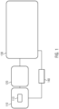
- FIG. 1 schematically shows a transmitter 100 for optical communication.
- the transmitter 100 comprises a pulse generation unit 110, a polarization state preparation unit 120, an active polarization state control unit 130, and an electronic control unit 140.
- the pulse generation unit 110 comprises a high bandwidth driven DFB laser 113 driven by an electrical pulse generator 111 and an electrical driver 112.
- the polarization state preparation unit 120 comprises a plurality of optical elements in a free-space configuration and is configured to transform an initial polarization state of an optical pulse generated by the pulse generation unit 110 into a superposition of two orthogonal polarization modes.
- the active polarization state control unit 130 is configured to time-demultiplex or spatially/optically demultiplex the two orthogonal polarization modes and individually apply a phase value to each of the orthogonal polarization modes. Embodiments of the active polarization state control unit 130 are described in the following with respect to Figures 2 and 3 .
- the electronic control unit 140 is configured to communicate with the pulse generation unit 110 and the active polarization state control unit 130.
- the electronic control unit 140 is further configured to generate signal patterns to control the pulse generation unit 110 and the active polarization state control unit 130 in order to generate an optical pulse with a desired polarization state. Examples of the signal patters are described with reference to Figures 4 and 5 below.
- FIG. 2 shows an embodiment of the active polarization state control unit 130 comprising a time-demultiplexing unit 131, a phase modulation unit 132, and a double pass unit 133.
- the time-demultiplexing unit 131 comprises a polarization based unbalanced polarization Mach-Zehnder interferometer (UMZI).
- the phase modulation unit 132 comprises an electro-optical modulator (EOM).
- EOM electro-optical modulator
- the double pass unit 133 comprises a Faraday mirror.
- the inbound path of an optical pulse through the active polarization state control unit 130 is indicated by the arrows in Figure 2 .
- An optical pulse comprising two orthogonal polarization modes first enters the time-demultiplexing unit 131, which separates the two orthogonal polarization modes by a time delay dt TDU , resulting in an early mode e, and a late mode I. This is indicated by the loops shown in the upper branch of the time-demultiplexing unit 131.
- the early mode e and the late mode I then pass through the phase modulation unit 132 at different times.
- the phase modulation unit 132 applies a pre-determined phase value individually to the modes e and I.
- the modes e and I pass through the double pass unit 133, which reflects the modes and inverts their polarization. This is indicated by the U-shaped arrow located near the double pass unit 133.
- the modes e and I then pass through the phase modulation unit 132 a second time, and a pre-determined phase value is applied individually to the modes e and I a second time.
- the modes e and I pass through the time-demultiplexing unit 131 in opposite direction, such that they re-combine again.
- the resulting optical pulse will have a polarization state that is determined by the phase values applied to the modes e and I in during their passes through the phase modulation unit 132.
- FIG 3 shows another embodiment of the active polarization state control unit 130 comprising a spatial demultiplexing unit 134.
- the spatial demultiplexing unit 134 comprises a UMZI with two optical branches. It can be seen that a phase modulator 135 is arranged in the lower of the optical branches of the UMZI.
- the phase modulator 135 may comprise an EOM. It is noted that the arrangement of the phase modulator 135 in the upper branch is merely illustrative. Further, it is possible that a second phase modulator (not shown) is arranged in the lower branch of the UMZI.
- the inbound path of an optical pulse through the active polarization state control unit 130 is also indicated by the arrows in Figure 3 .
- An optical pulse comprising two orthogonal polarization modes first enters spatial demultiplexing unit 134, which separates the two orthogonal polarization modes and sends it along the two different optical branches.
- the polarization mode passing through the lower branch of the UMZI passes through the phase modulator 135, and an individual phase is applied to the mode.
- the polarization modes are re-combined and reflected back by the double pass unit 133, in particular the Faraday mirror, for a second pass through the phase modulator 135. This is indicated by the U-shaped arrow located near the double pass unit 133.
- the resulting optical pulse will have a polarization state that is determined by the phase values applied to the mode passing through the phase modulator 135.
- Figure 4 schematically shows digital signal patterns generated by the electronic control unit 140 for an embodiment of the polarization state control unit 130 as illustrated in Figure 2 , where the time delay dt TDU added by the time-demultiplexing unit 131 is smaller than the total roundtrip time dt RT after the time-demultiplexing unit 131, dt TDU ⁇ dt RT .
- the signal patterns are digital signal patterns used to generate the final states
- the initial polarization state prepared, e.g., by the polarization state preparation unit 120 is the state
- the voltages applied to the phase modulation unit 132 are set to alternate between a first value V 1 and a second value V 2 whenever one of the modes e and I passes through the phase modulation unit 132. It can further be seen that the sequence of voltage values is inverted when comparing the sequence to obtain the final polarization state
- a total relative phase of ⁇ 2 is added between the modes e and I.
- L ⁇ a total relative phase of ⁇ ⁇ 2 is added between the modes e and I.
- the voltage value applied to the phase modulation unit 132 is kept at a constant value, thus that no relative phase is added between the modes a and I.
- Figure 5 schematically shows digital signal patterns generated by the electronic control unit 140 for an embodiment of the polarization state control unit 130 as illustrated in Figure 2 , where the time delay dt TDU added by the time-demultiplexing unit 131 is larger than the total roundtrip time dt RT after the time-demultiplexing unit 131, dt TDU > dt RT .
- the signal patterns are digital signal patterns used to generate the final states
- the initial polarization state prepared, e.g., by the polarization state preparation unit 120 is the state
- the horizontal axis denotes time. From top to bottom, Figure 5 shows:
- the voltage applied to the phase modulation unit 132 is set to a first value V 1 when the mode e passes through the phase modulation unit 132 for the first and second time, and to a second value V 2 when the mode I passes through the phase modulation unit 132 for the first and second time.
- the voltage applied to the phase modulation unit 132 is set to the second value V 2 when the mode e passes through the phase modulation unit 132 for the first and second time, and to the first value V 1 when the mode I passes through the phase modulation unit 132 for the first and second time.
- a ⁇ the voltage value applied to the phase modulation unit 132 is kept at a constant value.
- signal patterns are exemplary and different signal patterns may be used to obtain different final polarizations.
- a sequence resulting in a relative phase between the modes e and I would result in a final polarization state final polarization state
- the optical system can be used to prepare at least three different polarization states from an initial optical pulse.
- the system can, in particular, be used for the implementation of the BB84 protocol with three states.
- the voltage values may be adjusted gradually as the modes e and I pass through the phase modulation unit 132 instead of binary as shown in Figures 4 and 5 .
Landscapes
- Engineering & Computer Science (AREA)
- Physics & Mathematics (AREA)
- Electromagnetism (AREA)
- Computer Networks & Wireless Communication (AREA)
- Signal Processing (AREA)
- Optics & Photonics (AREA)
- Theoretical Computer Science (AREA)
- Computer Security & Cryptography (AREA)
- Optical Modulation, Optical Deflection, Nonlinear Optics, Optical Demodulation, Optical Logic Elements (AREA)
- Optical Communication System (AREA)
Priority Applications (2)
| Application Number | Priority Date | Filing Date | Title |
|---|---|---|---|
| EP22382931.8A EP4351043A1 (fr) | 2022-10-05 | 2022-10-05 | Système optique pour modulation de phase |
| US18/376,681 US20240137215A1 (en) | 2022-10-05 | 2023-10-04 | Optical System for Phase Modulation |
Applications Claiming Priority (1)
| Application Number | Priority Date | Filing Date | Title |
|---|---|---|---|
| EP22382931.8A EP4351043A1 (fr) | 2022-10-05 | 2022-10-05 | Système optique pour modulation de phase |
Publications (1)
| Publication Number | Publication Date |
|---|---|
| EP4351043A1 true EP4351043A1 (fr) | 2024-04-10 |
Family
ID=83691387
Family Applications (1)
| Application Number | Title | Priority Date | Filing Date |
|---|---|---|---|
| EP22382931.8A Pending EP4351043A1 (fr) | 2022-10-05 | 2022-10-05 | Système optique pour modulation de phase |
Country Status (2)
| Country | Link |
|---|---|
| US (1) | US20240137215A1 (fr) |
| EP (1) | EP4351043A1 (fr) |
Citations (2)
| Publication number | Priority date | Publication date | Assignee | Title |
|---|---|---|---|---|
| US6188768B1 (en) * | 1998-03-31 | 2001-02-13 | International Business Machines Corporation | Autocompensating quantum cryptographic key distribution system based on polarization splitting of light |
| US20040005056A1 (en) * | 2000-09-07 | 2004-01-08 | Tsuyoshi Nishioka | Optical signal transmitter and optical signal transmitting method |
Family Cites Families (31)
| Publication number | Priority date | Publication date | Assignee | Title |
|---|---|---|---|---|
| US4952014A (en) * | 1987-10-19 | 1990-08-28 | At&T Bell Laboratories | Optical systems with thin film polarization rotators and method for fabricating such rotators |
| US6175669B1 (en) * | 1998-03-30 | 2001-01-16 | The Regents Of The Universtiy Of California | Optical coherence domain reflectometry guidewire |
| JP3981969B2 (ja) * | 2000-07-31 | 2007-09-26 | 日本電気株式会社 | 量子回路 |
| US6577789B1 (en) * | 2001-09-26 | 2003-06-10 | Onetta, Inc. | Double-pass optical amplifiers and optical network equipment |
| US6690590B2 (en) * | 2001-12-26 | 2004-02-10 | Ljubisav S. Stamenic | Apparatus for regulating the delivery of power from a DC power source to an active or passive load |
| US20040208646A1 (en) * | 2002-01-18 | 2004-10-21 | Seemant Choudhary | System and method for multi-level phase modulated communication |
| US6897434B1 (en) * | 2002-02-28 | 2005-05-24 | Northwestern University | All-fiber photon-pair source for quantum communications |
| US7157687B1 (en) * | 2002-10-07 | 2007-01-02 | General Photonics Corporation | Optical devices with folded optical path designs |
| US7068411B2 (en) * | 2004-01-29 | 2006-06-27 | Lucent Technologies Inc. | Method and apparatus for optical sampling |
| CN1651947A (zh) * | 2004-02-02 | 2005-08-10 | 中国科学技术大学 | 一种偏振控制编码方法、编码器和量子密钥分配系统 |
| US8265280B2 (en) * | 2004-11-05 | 2012-09-11 | Nucrypt Llc | System and method of entangled photons generation |
| JP4795692B2 (ja) * | 2005-01-07 | 2011-10-19 | 株式会社日立製作所 | 光送信機、光送受信システム、および量子光生成器 |
| US20070196109A1 (en) * | 2006-02-22 | 2007-08-23 | Al-Chalabi Salah A | Secure optical communication system |
| US7289263B1 (en) * | 2006-08-02 | 2007-10-30 | Coherent, Inc. | Double-pass fiber amplifier |
| US7974534B2 (en) * | 2006-08-11 | 2011-07-05 | Purdue Research Foundation | Wideband microwave and millimeter wave filters using photonic spectral filtering |
| US20090185689A1 (en) * | 2008-01-18 | 2009-07-23 | Magiq Technologies, Inc. | QKD system and method with improved signal-to-noise ratio |
| FR2950746B1 (fr) * | 2009-09-30 | 2013-09-06 | Alcatel Lucent | Modulateur avec marquage de polarisation |
| JP5904694B2 (ja) * | 2009-12-10 | 2016-04-20 | 株式会社東芝 | サニャック干渉型光電流センサ |
| US8543000B2 (en) * | 2010-09-10 | 2013-09-24 | Fujitsu Limited | System and method for reducing polarization dependent loss cross-talk effects |
| US9720437B2 (en) * | 2012-05-10 | 2017-08-01 | The Mitre Corporation | Method and apparatus for quantum mechanical entanglement protection |
| KR101466213B1 (ko) * | 2012-10-18 | 2014-11-27 | 에스케이 텔레콤주식회사 | 양자 암호키 분배 시스템에 있어서 차동 광위상변조 방법 및 장치 |
| US9304257B2 (en) * | 2014-03-31 | 2016-04-05 | Lumentum Operations Llc | Wavelength selective switch using orthogonally polarized optical beams |
| US9876580B2 (en) * | 2014-04-22 | 2018-01-23 | Kabushiki Kaisha Toshiba | Optical device |
| US9531147B2 (en) * | 2014-11-21 | 2016-12-27 | Photonics Industries Int'l. | Pulse picking laser |
| WO2016191679A1 (fr) * | 2015-05-28 | 2016-12-01 | Massachusetts Institute Of Technology | Appareils et procédés de distribution quantique de clés |
| US10781688B2 (en) * | 2016-02-29 | 2020-09-22 | Halliburton Energy Services, Inc. | Fixed-wavelength fiber optic telemetry |
| US10382141B2 (en) * | 2017-07-12 | 2019-08-13 | The United States Of America, As Represented By The Secretary Of Commerce | Communication linker for communication linking |
| CN111082931B (zh) * | 2019-12-23 | 2021-04-20 | 清华大学 | 量子通信光路系统和量子通信方法 |
| EP4096509B1 (fr) * | 2020-01-31 | 2026-03-25 | The General Hospital Corporation | Génération de peigne de fréquences basée sur un verrouillage de mode de code de phase électro-optique pour tco à télémétrie circulaire |
| US11888978B1 (en) * | 2020-06-08 | 2024-01-30 | Cable Television Laboratories, Inc. | Systems and methods for measurement-device-independent quantum key distribution |
| WO2022035652A1 (fr) * | 2020-08-11 | 2022-02-17 | Chongchang Mao | Cristal liquide insensible à la polarisation sur silicium |
-
2022
- 2022-10-05 EP EP22382931.8A patent/EP4351043A1/fr active Pending
-
2023
- 2023-10-04 US US18/376,681 patent/US20240137215A1/en active Pending
Patent Citations (2)
| Publication number | Priority date | Publication date | Assignee | Title |
|---|---|---|---|---|
| US6188768B1 (en) * | 1998-03-31 | 2001-02-13 | International Business Machines Corporation | Autocompensating quantum cryptographic key distribution system based on polarization splitting of light |
| US20040005056A1 (en) * | 2000-09-07 | 2004-01-08 | Tsuyoshi Nishioka | Optical signal transmitter and optical signal transmitting method |
Non-Patent Citations (5)
| Title |
|---|
| GISIN, NICOLAS ET AL.: "Quantum cryptography", REVIEWS OF MODERN PHYSICS, vol. 74, no. 1, 2002, pages 145 |
| GRUNENFELDER, F.BOARON, A.RUSCA, D.MARTIN, A.ZBINDEN, H.: "Performance and security of 5 GHz repetition rate polarization-based quantum key distribution", APPLIED PHYSICS LETTERS, vol. 117, no. 14, 2020, pages 144003, XP012250675, DOI: 10.1063/5.0021468 |
| KO, HEASIN ET AL.: "High-speed and high-performance polarization-based quantum key distribution system without side channel effects caused by multiple lasers", PHOTONICS RESEARCH, vol. 6, no. 3, 2018, pages 214 - 219 |
| LO, HOI-KWONGXIONGFENG MAKAI CHEN: "Decoy state quantum key distribution", PHYSICAL REVIEW LETTERS, vol. 94, no. 23, 2005, pages 230504 |
| WANG, JINGBERNARDO A. HUBERMAN: "Future of Information and Communication Conference", 2022, SPRINGER, article "A Guide to the Deployment of Global Quantum Key Distribution Networks" |
Also Published As
| Publication number | Publication date |
|---|---|
| US20240137215A1 (en) | 2024-04-25 |
Similar Documents
| Publication | Publication Date | Title |
|---|---|---|
| US8374350B2 (en) | Quantum communication system | |
| EP4178152A1 (fr) | Système de communication quantique ayant des impulsions divisées en segments temporels et procédés associés | |
| JP2951408B2 (ja) | 量子暗合化システムおよび方法 | |
| US9401766B2 (en) | Quantum communication network | |
| US8433070B2 (en) | Systems and methods for stabilization of interferometers for quantum key distribution | |
| CN104092538B (zh) | 多用户波分复用qkd网络系统及其密钥分发与共享方法 | |
| JP2019522434A (ja) | 位相偏波多自由度変調qkdネットワークシステム及びその方法 | |
| CN103546280A (zh) | 用于量子密码通信的编码器和解码器 | |
| JP2014147068A (ja) | 変調ユニット | |
| EP4096120B1 (fr) | Émetteur, système et procédé de communication | |
| EP4178123B1 (fr) | Système de communication quantique ayant au moins une lame d'onde pour modifier la polarisation d'impulsion et procédés associés | |
| WO2022189523A1 (fr) | Émetteur de distribution de clé quantique | |
| EP4096119B1 (fr) | Émetteur optique, système et procédé de communication | |
| EP4351043A1 (fr) | Système optique pour modulation de phase | |
| Kumavor et al. | Experimental multiuser quantum key distribution network using a wavelength-addressed bus architecture | |
| US12225116B1 (en) | Quantum key distribution network with centralized optical pulse generation | |
| Agnesi et al. | Time-bin Quantum Key Distribution exploiting the iPOGNAC polarization moulator and Qubit4Sync temporal synchronization | |
| US20260121843A1 (en) | Method and system for ongoing spectral feedback and control during quantum key distribution using data analysis | |
| RU2814445C1 (ru) | Система квантовой криптографии на запутанных поляризационных состояниях фотонов с активным выбором базиса измерения | |
| Agnesi et al. | Simple and robust QKD system with Qubit4Sync temporal synchronization and the POGNAC polarization encoder | |
| EA052235B1 (ru) | Система квантовой криптографии на запутанных поляризационных состояниях фотонов с активным выбором базиса измерения | |
| STEFANESCU et al. | QUANTUM CRYPTOGRAPHY IN CHAOTIC SYNCHRONIZED SYSTEMS | |
| Bogdanski et al. | Sagnac quantum key distribution over telecom fiber networks | |
| Kumavor et al. | Demonstration of a six-user quantum key distribution network on a bus architecture | |
| WO2024181891A1 (fr) | Système de cryptographie quantique avec sélection active de la base de mesure |
Legal Events
| Date | Code | Title | Description |
|---|---|---|---|
| PUAI | Public reference made under article 153(3) epc to a published international application that has entered the european phase |
Free format text: ORIGINAL CODE: 0009012 |
|
| STAA | Information on the status of an ep patent application or granted ep patent |
Free format text: STATUS: THE APPLICATION HAS BEEN PUBLISHED |
|
| AK | Designated contracting states |
Kind code of ref document: A1 Designated state(s): AL AT BE BG CH CY CZ DE DK EE ES FI FR GB GR HR HU IE IS IT LI LT LU LV MC ME MK MT NL NO PL PT RO RS SE SI SK SM TR |
|
| STAA | Information on the status of an ep patent application or granted ep patent |
Free format text: STATUS: REQUEST FOR EXAMINATION WAS MADE |
|
| 17P | Request for examination filed |
Effective date: 20241004 |
|
| RBV | Designated contracting states (corrected) |
Designated state(s): AL AT BE BG CH CY CZ DE DK EE ES FI FR GB GR HR HU IE IS IT LI LT LU LV MC ME MK MT NL NO PL PT RO RS SE SI SK SM TR |