EP4354082A2 - Dispositif micromécanique de mesure et de stockage autonome en énergie d'un signal de déplacement mécanique - Google Patents
Dispositif micromécanique de mesure et de stockage autonome en énergie d'un signal de déplacement mécanique Download PDFInfo
- Publication number
- EP4354082A2 EP4354082A2 EP24153189.6A EP24153189A EP4354082A2 EP 4354082 A2 EP4354082 A2 EP 4354082A2 EP 24153189 A EP24153189 A EP 24153189A EP 4354082 A2 EP4354082 A2 EP 4354082A2
- Authority
- EP
- European Patent Office
- Prior art keywords
- locking
- mechanical
- strain
- displacement
- maximum value
- Prior art date
- Legal status (The legal status is an assumption and is not a legal conclusion. Google has not performed a legal analysis and makes no representation as to the accuracy of the status listed.)
- Pending
Links
Images


Classifications
-
- G—PHYSICS
- G01—MEASURING; TESTING
- G01B—MEASURING LENGTH, THICKNESS OR SIMILAR LINEAR DIMENSIONS; MEASURING ANGLES; MEASURING AREAS; MEASURING IRREGULARITIES OF SURFACES OR CONTOURS
- G01B5/00—Measuring arrangements characterised by the use of mechanical techniques
- G01B5/30—Measuring arrangements characterised by the use of mechanical techniques for measuring the deformation in a solid, e.g. mechanical strain gauge
-
- G—PHYSICS
- G01—MEASURING; TESTING
- G01B—MEASURING LENGTH, THICKNESS OR SIMILAR LINEAR DIMENSIONS; MEASURING ANGLES; MEASURING AREAS; MEASURING IRREGULARITIES OF SURFACES OR CONTOURS
- G01B21/00—Measuring arrangements or details thereof, where the measuring technique is not covered by the other groups of this subclass, unspecified or not relevant
- G01B21/32—Measuring arrangements or details thereof, where the measuring technique is not covered by the other groups of this subclass, unspecified or not relevant for measuring the deformation in a solid
-
- G—PHYSICS
- G01—MEASURING; TESTING
- G01B—MEASURING LENGTH, THICKNESS OR SIMILAR LINEAR DIMENSIONS; MEASURING ANGLES; MEASURING AREAS; MEASURING IRREGULARITIES OF SURFACES OR CONTOURS
- G01B5/00—Measuring arrangements characterised by the use of mechanical techniques
- G01B5/0011—Arrangements for eliminating or compensation of measuring errors due to temperature or weight
- G01B5/0014—Arrangements for eliminating or compensation of measuring errors due to temperature or weight due to temperature
-
- G—PHYSICS
- G01—MEASURING; TESTING
- G01B—MEASURING LENGTH, THICKNESS OR SIMILAR LINEAR DIMENSIONS; MEASURING ANGLES; MEASURING AREAS; MEASURING IRREGULARITIES OF SURFACES OR CONTOURS
- G01B7/00—Measuring arrangements characterised by the use of electric or magnetic techniques
- G01B7/16—Measuring arrangements characterised by the use of electric or magnetic techniques for measuring the deformation in a solid, e.g. by resistance strain gauge
-
- G—PHYSICS
- G06—COMPUTING OR CALCULATING; COUNTING
- G06M—COUNTING MECHANISMS; COUNTING OF OBJECTS NOT OTHERWISE PROVIDED FOR
- G06M1/00—Design features of general application
- G06M1/08—Design features of general application for actuating the drive
- G06M1/083—Design features of general application for actuating the drive by mechanical means
-
- G—PHYSICS
- G06—COMPUTING OR CALCULATING; COUNTING
- G06M—COUNTING MECHANISMS; COUNTING OF OBJECTS NOT OTHERWISE PROVIDED FOR
- G06M1/00—Design features of general application
- G06M1/27—Design features of general application for representing the result of count in the form of electric signals, e.g. by sensing markings on the counter drum
Definitions
- the present invention relates to a device and a method for spatially resolved strain measurement at specific points on a mechanically stressed component.
- the invention particularly relates to a device for mechanical strain measurement via two connecting elements, the displacement of which is amplified by a mechanical amplifier and converted into an electrical value by an electromechanical converter.
- the invention also relates to mechanical maximum value storage and the associated possibility of energy-autonomous strain monitoring.
- Strain gauges are often used to monitor components subject to high levels of stress. Strain gauges can be used to determine strains and stresses at specific points on a mechanically stressed component with local resolution. Strain gauges are strain-sensitive electrical resistors whose resistance value increases with increasing strain or decreases with increasing compression. By measuring the resistance, the current strain can be determined extremely precisely.
- strain measurements on macroscopic components are carried out using resistive strain gauges (SGS) and piezoresistive strain measuring systems.
- the k-factor is in the range of 1.5 to 3.
- Semiconductors reach values between 20 and 100 (Schomburg, 2011; Gerlach and Dötzel, 2006). The sensitivity of the resistance change to the strain is therefore very small even at very high strains of 1%.
- strain gauges are always connected in a "Wheatstone measuring bridge" to compensate for the influence of temperature. If a quarter or half bridge is used as the measuring bridge, the strain sensitivity is also reduced to a quarter or half.
- a complex analog circuit is also required to evaluate the changes in resistance or the bridge voltage. Instrument amplifiers are usually used to amplify the weak analog electrical measurement signal (Tietze et al. 2012).
- an offset correction of the bridge voltage almost always has to be carried out, since the resistance values of the reference resistors in the measuring bridge are not identical due to manufacturing reasons and this usually results in an offset voltage on the measuring bridge.
- strain gauges Further details on strain gauges can be found in VDI/VDE 2635 Sheet 1 and Sheet 2.
- Another way of measuring strain is to attach fiber Bragg gratings to the component to be stretched.
- a light beam is introduced into an optical fiber with a fiber Bragg grating and spectrally analyzed at the other end of the conductor.
- the spectral shift of the reflected wavelength can be used to obtain information about the change in length of the conductor (Chen et al .; DE 10214984 B4 ; EP2294374B1 ; EN 102014004544 T5 ).
- FBG fiber Bragg gratings
- Light that is guided through the optical waveguide is reflected at the optical interfaces of the modified areas depending on the wavelength. The reflection of certain wavelengths results from the phase shift of the reflected light wave by 180° or 0° when it hits an optical interface.
- phase shift depends on whether the light first comes from an area with a high refractive index and hits an area with a low refractive index (0°) or whether it conversely hits an area with a low refractive index from an area with a high refractive index (180°).
- extensometers are often used to determine the strain on tensile specimens. Strain measurement is usually carried out optically and without contact and without sticking on strain gauges or FBGs. To determine the strain, markings are provided on the tensile specimen, which are optically recorded, for example, via video analysis. The displacement of the markings allows information to be obtained about the strain of the test specimen. Alternatively, interferometric principles can also be used to measure the strain. An overview of the various methods is provided by Tian et al. (2012) and EN 102010038062 B9 , EN 102015002452 T5 .
- the sensor unit in EN 69822097T2 It is a device for measuring a displacement or extension using two "electrode arrays" that can be moved relative to one another.
- the electrode arrays have a corresponding vernier structure for high-resolution measurement of the displacement.
- different electrodes are placed on top of one another.
- the electrodes themselves do not touch one another. Only a change in charge of the changed capacitance of the individual electrodes is registered. The change in the charges is converted into a digital signal using an electronic evaluation unit.
- the DE 102016202769 A1 discloses a sensor for integral or spatially resolved measurement of strains based on pre-damaged carbon fibers.
- the carbon fibers are embedded in a hardened matrix and are electrically contacted from two sides.
- the electrical resistance changes due to the stretching of the carbon fibers. If the breaking stress If the maximum stretch value of individual carbon fibers is reached during stretching, the resistance increases significantly.
- the maximum stretch value reached can be stored passively. However, there is no way to reset the stored maximum value.
- a passive device for counting strain exceedances is used in the EP 2 705 330 B1 This is a three-dimensional measuring device for attachment to a test object via two fixing points. When a specified strain limit is exceeded, the number of strain cycles is counted via a gear-based mechanism. However, the maximum strain achieved is not recorded. A gear-based mechanism also always has play, which distorts a continuous strain measurement.
- strain gauges allows continuous monitoring of the stresses that occur. Often, however, only the maximum strain peaks reached are of interest, particularly for maintenance purposes, so that the continuously recorded data is usually not needed at all and is therefore discarded.
- component monitoring using strain gauges is extremely complex, since the strain gauges are connected in a measuring bridge for temperature compensation and the signals on the measuring bridges must be processed. In addition to the electrical amplification of the bridge voltage and the offset correction, digitization and often also storage of the measurement results is required. Furthermore, a power supply is necessary for the measurement, which entails cabling of the strain gauges and the evaluation electronics.
- One object of the present invention was therefore to provide a novel micromechanical system as an alternative to classical resistance-based strain gauges, which allows continuous mechanical component monitoring in a completely energy-autonomous manner.
- a further object of the present invention was to ensure mechanical maximum value storage with such a micromechanical system and thus to enable energy-autonomous strain monitoring.
- microsystems presented here can be attached to a sample in the form of a chip for local strain monitoring in order to measure and store the current strain or the maximum strain that occurs.
- a resistance bridge with a corresponding amplifier circuit with offset correction and an electronic A/D converter are not required with this principle.
- the strain is measured purely mechanically, so that electrical parasitic effects such as thermal noise play only a minor role in contrast to resistive strain gauges.
- the micromechanical system according to the invention has the advantage over existing strain measurement systems that no continuous power supply is required for continuous monitoring using a maximum value memory and the system can be used completely self-sufficiently in terms of energy. No complex electrical amplifier circuit and no wiring in a measuring bridge are necessary, and thus no balancing of resistors.
- the system directly discretizes and digitizes the measured values in the mechanical domain. Since strain detection is a purely mechanical principle, there are no parasitic electrical effects (such as thermal noise).
- the system according to the invention is also inexpensive to manufacture, as it is preferably based on a standardized SOI technology (with many chips per wafer). Since essentially only silicon and metals, glasses or ceramics are used in production, the system is temperature-stable and environmentally friendly. There are many different options for mechanically connecting the system to a test object, e.g. by soldering, welding, gluing or bonding.
- the present invention relates to a micromechanical strain measuring system that makes it possible to determine strains on stressed components or tensile specimens with local resolution.
- the strain measurements can be used both for continuous monitoring of maintenance-intensive components and for classic material testing tests (tensile test, fatigue strength test).
- the strain measuring system according to the invention allows continuous measurement and query of the current strain on a specimen with a continuous power supply.
- the sensor already supplies a discrete or digital, preferably electrical signal.
- the strain measuring system according to the invention can be designed in such a way that it continuously monitors the strain on a component even without an electrical power supply and stores the maximum strain value achieved in a mechanical memory. Electrical energy is not required for this.
- the stored measured value can later be queried electronically at any time, e.g. via RFID ("radio-frequency identification").
- the strain measuring system according to the invention can be designed in such a way that it is possible to delete the mechanical maximum value memory in the chip with an electrical pulse in order to reset the sensor.
- the present invention relates in particular to a micromechanical measuring system for measuring strains on macroscopic objects comprising at least two connecting elements (1a, 1b) for fixing the measuring system to the measuring object to be examined and/or monitored, wherein at least one connecting element is connected to the substrate of the measuring system in a frame-fixed manner and at least one connecting element is connected directly or indirectly to the input of a mechanical amplifier, a mechanical amplifier (2) for signal amplification of the strain-induced mechanical displacement, and an electromechanical signal converter (3) for converting the amplified mechanical displacement into an electrical analog or digital signal.
- a preferred subject of the present invention is said micromechanical measuring system, which further comprises a mechanical maximum value memory (4) for mechanically storing the maximum achieved elongation of the measuring object.
- Said mechanical maximum value memory comprises a coupling (6).
- said mechanical maximum value memory (4) is based on ratchet teeth.
- a further preferred subject matter of the present invention is said micromechanical measuring system with mechanical ratchet-based maximum value memory (4), further comprising a reset mechanism (5) for erasing the mechanical maximum value memory.
- a further preferred subject matter of the present invention is said micromechanical measuring system, which further comprises a compensation mechanism (14) which is designed to compensate for an isotropic strain of a measuring object (12) and to decouple it from an axially acting strain signal.
- connecting elements in the sense of the present invention refers to devices and components that serve to connect the micromechanical measuring system and the component to be examined.
- the connecting elements have Measuring system has firmly defined positions and distances. At least one connecting element is firmly connected to the substrate of the microsystem, while at least one other can be moved translationally relative to the substrate.
- a "mechanical amplifier” in the sense of the present invention is understood to mean a component whose task is to convert an initially small translational displacement into a translational displacement with a high amplitude in order to enable a sensitive resolution of the strain.
- An “electromechanical signal converter” in the sense of the present invention is understood to mean a component whose task is to mechanically discretize the displacement at the output of the amplifier and to convert it into a discrete, preferably binary-coded electrical signal.
- a "mechanical maximum value memory” in the sense of the present invention is understood to mean a device or a component whose task is to mechanically store the maximum strain reached in discrete steps. In this way, continuous strain monitoring can be carried out without a power supply having to be continuously available. The strain value stored in the maximum value memory is always overwritten if a higher strain amplitude is registered than was previously stored.
- a "macroscopic object” in the sense of the invention is understood to be an object whose smallest geometric dimensions are larger than those of the measuring device according to the invention.
- a “measurement object” in the sense of the invention is understood to be any objects, items or components that can or should be subjected to a strain measurement or strain monitoring.
- a “flexible housing” in the sense of the invention is understood to mean a component which has a low modulus of elasticity compared to the measuring object and which is designed to transfer the strain of the measuring object to the connecting elements of the strain sensor with negligible resistance.
- a “substrate of the micromechanical strain measuring system” in the sense of the invention is understood to mean the mechanical frame of the strain sensor, i.e. a device that serves as a carrier and/or for fastening.
- a “sacrificial layer” in the sense of the invention is understood to be a material layer required for the production of the strain sensor, which mechanically connects the device layer and the handle layer and which is partially removed to expose the movable structures on the device layer.
- axial strain or "axially acting strain” in the sense of the invention is understood to mean the direction of a strain along the sensitive axis of the strain sensor according to the invention in whose direction the strain effect is to be detected.
- a “compensation mechanism” in the sense of the invention is understood to mean a component which is designed to compensate for the isotropic strain when isotropic and axial strains are superimposed and to separate it from the axial strain.
- a "mechanical input transducer” in the sense of the invention is understood to mean a component which is designed to convert a physical quantity to be measured into a displacement or strain quantity which in turn causes a relative displacement of the frame-fixed (1b) and flexible connecting elements (1a).
- a “passive” measurement/conversion or a “passive” component in the sense of the invention is understood to mean a method or device in which no active power or energy amplification of an output signal takes place.
- An “energy-autonomous" measurement or an “energy-autonomous” storage in the sense of the invention is understood to mean a method in which a physical quantity is measured and/or stored without additional external auxiliary energy. The energy for the measurement and/or storage is obtained directly from the energy of the measurement signal.
- the connecting elements (1a, 1b) of the micromechanical measuring system are arranged at a known distance on the measuring system, with at least one connecting element being connected to the substrate of the measuring system in a frame-fixed manner and at least one further element being mounted on the measuring system in a spring-loaded manner so as to be translationally or rotationally displaceable. It can be mechanically connected to the mechanical amplifier directly or indirectly via a coupling.
- the mechanical amplifier (2) converts a translational movement on the input side into an amplified, likewise translational displacement on the output side.
- the amplifier is designed to carry out a path amplification with either a constant amplification factor or a path amplification with a strain-dependent amplification.
- the mechanical amplifier is designed to implement a predefined transfer function of the amplification depending on the translational displacement on the input side and to apply it to the displacement signal on the output side.
- the strain-induced amplified displacement can be converted into a digital or analog electrical quantity, in particular via an electromechanical converter.
- the electromechanical converter is designed in the form of an electromechanical analog-digital converter (3) which is designed to convert a shift at the output of the amplifier into a discrete binary-coded parallel electrical voltage signal.
- the output binary code is preferably a dual code, Gray code, BCD code, unary code, Aiken code, Libaw-Craig code or sum code, but other binary codings are also conceivable.
- a further embodiment of the micromechanical measuring system according to the invention provides that a predefined transfer function is applied to the primary measuring signal at the input of the amplifier or the electromechanical transducer via the micromechanical amplifier and/or via the electromechanical transducer.
- the micromechanical measuring system is designed such that the maximum displacement achieved at the output of the mechanical amplifier can be fixed by a multi-stage locking mechanism.
- the micromechanical measuring system according to the invention can be designed in such a way that it carries out an autonomous continuous strain measurement of the measuring object even without a continuous electrical energy supply and stores the maximum strain value achieved in the form of a fixed displacement via a mechanical ratchet-based maximum value memory.
- a compensation mechanism (14) can be implemented on the measuring system, in particular on the flexible connecting element (1a), which is designed to compensate for a possible thermally induced isotropic strain on the measuring object (12) and to decouple it from an axially acting strain signal.
- the micromechanical measuring system can be extended by a mechanical input transducer (16) in order to record, store and/or discretize and digitize other physical measurement variables, in particular acceleration, voltage, current, magnetic field strength, electric field strength or humidity, instead of the strain on a test object.
- the connecting elements (1a, 1b) can be attached to the "handle layer” and/or the "device layer”.
- the "handle layer” and the “device layer” contain silicon and/or an additional layer ("BOX layer”) located therebetween contains silicon dioxide, which acts as a sacrificial layer.
- the fabrication of the micromechanical measuring system according to the present invention is carried out by means of lithography and/or by anisotropic etching.
- the micromechanical measuring system can be implemented in the form of a silicon chip.
- the production of the micromechanical measuring system is extended in that at least the connecting elements (1a, 1b) are materially connected to a further substrate that serves as a flexible housing (11).
- a solder and/or reactive metal layers and/or an adhesive can be deposited and structured on the surface of the flexible housing (11) or directly on the connecting elements.
- the calculation of the strain of the measuring object from the known distance of the connecting elements and the amplified signal of the distance change is carried out via the output electrical signal.
- the method according to the invention can comprise a further step between said steps (iii) and (iv), namely the storage of the maximum value of the strain achieved in a mechanical maximum value memory.
- the method according to the invention can be designed in such a way that an autonomous continuous strain measurement of the measuring object is carried out without continuous electrical energy supply and the maximum strain value achieved is stored in the form of a fixed displacement via a mechanical ratchet-based maximum value memory.
- the method according to the invention can comprise a further step between said steps (ii) and (iii), in which the existing displacement at the input of the electromechanical transducer is fixed by applying a voltage for the duration of the conversion of the displacement into an electrical quantity and is released again after completion of the signal conversion.
- the method according to the invention can comprise a further step between said steps (i) and (ii) in which a uniaxial strain in the direction of the sensitive measuring axis of the strain sensor is decoupled from a superimposed isotropic strain of the measuring object via a compensation mechanism and only the uniaxial strain is transmitted to the micromechanical amplifier.
- Fig.1 shows the main components of the micromechanical strain measuring system (10) and their arrangement comprising at least two connecting elements (1a, 1b), wherein a connecting element (1b) is connected to the substrate of the micromechanical strain measuring system (13) in a frame-fixed manner and at least one further connecting element is flexibly mounted relative to the substrate of the micromechanical strain measuring system (13) and the geometric distance between all connecting elements is known.
- the connecting elements establish a mechanical coupling between the micromechanical strain measuring system (10) and the measurement object (12).
- the micromechanical strain measuring system also comprises a mechanical amplifier (2) and an electro-mechanical signal converter (3).
- the strain sensor also includes a coupling (6) and a mechanical maximum value memory (4) in an extended version.
- the order and arrangement of the main components can vary.
- the application and handling of the micromechanical strain measuring system is similar to that of a strain gauge.
- the strain sensor (10) is, as in Fig.2 shown, in the form of a chip, it is glued/joined in a form-fitting manner to the surface of a measuring object (12) to be examined.
- the chip is connected to the workpiece via at least two defined points, the connecting elements (1a, 1b).
- the distance between the connecting elements (1a, 1b) is precisely known and is determined by a geometry on the chip.
- At least one of the connecting elements is softly mounted on the chip via spring elements (1a) and can be moved translationally or rotationally with little effort.
- the other connection point (1b) is rigidly and frame-fixedly connected to the substrate/frame of the chip.
- both connecting elements are mechanically connected to the measuring object (12), as in Fig.3 shown.
- the chip is not mounted directly on the measuring object (12), but as in Fig.4 shown indirectly via a flexible housing (11).
- a flexible circuit board is used, on which the micromechanical strain measurement system (10) is mounted via the two connecting elements (1a, 1b).
- the flexible housing (11) is in turn attached to the measuring object (12).
- the flexible housing first absorbs the strain of the measuring object (12) and then transfers it to the actual strain sensor.
- the housing is an advantageous extension to protect the mechanical strain sensor from dirt or moisture or to optimize the assembly of the "strain sensor and housing" assembly, e.g. by means of large adhesive surfaces.
- Glass, silicon, ceramic or glass-ceramic substrates are particularly suitable as materials for the flexible housing.
- the use of a material with a thermal expansion coefficient adapted to the measurement object (12) is also conceivable.
- the micromechanical strain measuring system (10) can preferably be hermetically sealed and connected to the flexible housing (11) using anodic, eutectic or fusion bonding. By choosing the material for the flexible housing (11), the difference in thermal linear expansion between the measurement object and the micromechanical strain measuring system is taken into account during the measurement and can thus be compensated in order to prevent thermally induced mechanical stress in the measuring system.
- Fig.5 shows a possible embodiment of the strain sensor (10).
- the connecting elements (1a, 1b) are displaced relative to one another on the chip using the micromechanical strain measuring system.
- the relative displacements experienced by the connection points/connecting elements are very small, as can be seen in the example above, so that the displacement amplitude (here 10 ⁇ m) must be amplified by a mechanical amplifier (2) in the form of a lever mechanism.
- a mechanical amplifier (2) is used, which converts the small displacement at the amplifier input (2.1) into a larger displacement at the amplifier output (2.2).
- the amplified displacement is transmitted at the output to a translatory-guided rotor (8).
- the mechanical amplifier (2) is also designed to implement a predefined transfer function of the gain depending on the displacement. In addition to a constant path gain, non-linear gain curves are also achieved. depending on the input displacement. With the help of the amplifier (2) it is thus possible to adapt the sensitivity curve of the strain measurement for different value ranges.
- an electromechanical signal converter (3) is implemented at the output of the mechanical amplifier (2).
- a geometric coding in the form of contact electrodes (3.1.1) can be engraved on the rotor (8) that is mounted on the amplifier output (2.2).
- several frame-fixed but flexibly mounted counter electrodes (3.1.2) can be located next to the rotor (8), which either come into contact with the contact electrodes on the rotor or move very close to them as soon as the rotor is moved translationally.
- the electrodes mounted on the rotor (3.1.1) and the electrodes mounted on the frame (3.1.2) are initially galvanically isolated when the rotor is not deflected.
- an electrical direct or alternating voltage U 0 is introduced and applied to the rotor (8), for example via a conductive guide spring (7).
- the voltage is tapped at the contact electrodes (3.1.2) fixed to the frame and measured.
- the electrical potential at the counter electrodes (3.1.2) is pulled to a known and fixed potential via high-resistance pull-down or pull-up resistors (3.1.5), as long as the counter electrodes (3.2.1) fixed to the frame do not touch the movable finger electrodes on the rotor (3.1.1).
- the strain sensor as described above is capable of continuously carrying out strain measurements. No values are stored mechanically yet.
- the strain measurement is therefore only active as described above, i.e. only possible using an electrical energy source.
- continuous querying of the measured values is often not necessary. Often the information as to whether a certain maximum strain value has been reached or exceeded is sufficient.
- a mechanical maximum value memory (4) is implemented on the rotor in addition to the electromechanical converter. This comprises, as shown in Fig.6 shown, one or more frame-fixed locking blades (4.2) and locking elements (4.1) with associated locking teeth (4.3), which fix the rotor in its maximum reached position.
- the maximum value memory can optionally be designed in such a way that it can be reset to its original state via a reset mechanism (5), whereby the stored maximum value is deleted.
- a coupling (6) can therefore be installed between one of the connecting elements (1a, 1b) and the mechanical maximum value memory (4). be implemented.
- the coupling (6) is designed to selectively transmit a force introduced by the connecting element to the mechanical maximum value memory (4) only in a direction intended for it.
- the strain sensor as previously described is able to detect strains of a measurement object without distinguishing between mechanically induced uniaxial strain and thermally induced isotropic strain as a result of thermal expansion.
- the device according to the invention is therefore expanded to include a compensation mechanism (14) which is designed to compensate for the isotropic thermal expansion of a measurement object and to decouple it from a uniaxial strain signal of the measurement object, so that purely mechanically induced temperature-independent strain measurements are possible.
- Fig. 7A shows a possible structure of the compensation mechanism (14).
- the compensation mechanism (14) is symmetrical and is installed between the amplifier input (2.1) and the flexibly mounted connecting element (1a). Any positioning within the measuring device is also possible.
- the compensation mechanism (14) comprises at least one additional flexibly mounted connecting element (1c, 1d) and at least one deflection mechanism (14.2) which is designed to transform a displacement of the connecting element (1c, 1d) in the lateral direction into a displacement in the longitudinal direction.
- the mechanism comprises a force transformer (14.1), for example in the form of a spring, which is designed to convert a displacement into a force F.
- Fig. 7A also shows the function of the compensation mechanism (14): If the measuring object (12) to be monitored expands isotropically, i.e. evenly in all directions, e.g. due to a change in temperature, the distance between the connecting elements (1a, 1b) changes in the longitudinal direction (y-direction) and the distance between the connecting elements (1c, 1d) changes in the lateral direction (x-direction). The lateral displacement of the additional connecting elements (1c, 1d) is turned into a longitudinal displacement via the deflection mechanism (14.2) and converted into a force F 1 in the longitudinal direction via the force transformer (14.1). (y-direction). The force F 1 is then applied directly or indirectly to the input of the mechanical amplifier (2.1).
- the flexibly mounted connecting element (1a) is also connected to the input of the amplifier (2.1) via a force transformer (14.1).
- a force F 2 that is equal in magnitude to but opposite to the force F 1 is generated via the flexibly mounted connecting element (1a) and the associated force transformer (14.1), so that the resulting forces at the amplifier input (2.1) compensate and there is no displacement y in the amplifier input (2.1).
- the isotropic expansion is therefore not amplified by the amplifier.
- Fig.8 shows a simplified embodiment in which the compensation mechanism (14) is mounted on the measuring device according to the invention without a maximum value memory.
- the compensation mechanism (14) can also be operated in combination with a maximum value memory.
- the order and interconnection of the components can vary.
- the device according to the invention as described so far can also be used to measure other physical quantities instead of strain measurement by means of a simple modification.
- the flexibly mounted connecting element (1a) is not connected directly to the test object (12), but to a mechanical input transducer (16). It is conceivable, for example, that in order to measure and store the amplitude of an acceleration effect on a test object (12), only the frame-mounted connecting element (1b) is mounted on the test object, while the flexibly mounted connecting element (1a) is connected to a seismic test mass (16.1).
- the deflection of the test mass (16.1) also causes a relative displacement between the frame-mounted and flexible connecting elements (1a, 1b), which is recorded, amplified, stored and directly digitized in accordance with the sensor and storage concept of the device according to the invention.
- the connecting elements (1) serve to connect the strain sensor (10) and the measurement object (12) to be examined or the housing (11) located between the measurement object (12) and the strain sensor (10).
- the connecting elements (1a, 1b) have fixed positions and distances on the strain sensor (10). The greater the distance between the connecting elements, the more sensitive the strain measurement, but the less precise the spatial resolution of the strain measurement.
- At least one connecting element is firmly connected to the substrate of the microsystem (1b), while at least one other is mounted so that it can be moved in translation relative to the substrate/frame (1a), e.g. via solid-state joints or guide springs.
- the strain of the test object is transmitted to the strain sensor (10) in the form of a displacement via the connecting elements.
- the surface of the connecting elements differs from the remaining surfaces of the micromechanical measuring system in that they have a surface topology and morphology optimized for joining.
- an additional adhesion promoter is deposited on the connecting surfaces, which allows the connecting elements to be locally bonded or soldered to a workpiece or test object, while the other surfaces of the chip are not wetted by the solder or adhesive. It is also possible to deposit solder, adhesive or reactive layers made of e.g. Ni/Al on the connecting surfaces in order to implement a local welding process.
- the mechanism is symmetrical and comprises at least two levers (2.3.1) arranged in parallel on each side.
- Each lever (2.3.1) is mounted in a rotational manner relative to the frame/substrate (13).
- the levers (2.3.1) are coupled to each other in pairs on one side via a lever connector (2.3.2).
- the multiplicative link makes it possible to achieve relatively high gain factors of preferably 1...1000 and to implement the amplifier in a very small space.
- the gain factor A total depends on its segment lengths a, b, c and d:
- a total y out y in ⁇ b a ⁇ d c
- Fig.10 shows another embodiment of the mechanical amplifier.
- m levers are connected in series via lever connectors.
- a total y out
- the joints of the two-dimensional reinforcement mechanism implemented using microsystems technology can be implemented in the form of solid-state joints in order to avoid abrasion on the joint axes.
- Sliding joints at the input and output can be dispensed with in this case, since the restoring forces of the solid-state joints and the symmetrical structure of the mechanism compensate for any transverse forces at the input or output.
- a translational displacement on the input side is thus converted into a purely translational displacement at the output. Additional sliding joints are therefore optional when using solid-state joints.
- the stiffness of the amplifier is determined by the stiffness c i of the solid joints and the reinforcement of the individual levers. The stiffer the system input, the higher the force that must be applied to move the input element of the amplifier.
- Fig. 11 shows an extended version of the amplifier (2) with implemented transfer function, which allows to apply a displacement-dependent gain factor to the input-side displacement in addition to a constant gain factor.
- the gain A total ( y in ) is a function of the input shift y in .
- a quadratically increasing strengthening of the form A total y in A total ⁇ y in 2 as well as logarithmic or root functions can be implemented on the amplifier.
- At least one of the joints on the lever mechanism that connects the lever mechanism to the substrate is replaced by at least one cam disk (2.3.4), with the predefined transfer function being implemented on the cam disk (2.3.4).
- the associated lever (2.3.1) When the associated lever (2.3.1) is deflected, it is not rotated about a point fixed to the substrate defined by a fixed joint, but moves along the cam disk (2.3.4). Since the lever slides along the cam disk, the pivot point also moves depending on the displacement, whereby the associated distance a or b or c or d and thus the gain changes depending on the displacement, as in Fig. 12 will be shown.
- the task of the electromechanical converter (3) is to convert the displacement at the output of the amplifier (2.2) into an electrical signal.
- the displacement can be measured using a capacitive converter (3.3), as in Fig. 13 shown.
- a capacitive converter 3.3
- isolated, freely movable electrodes can be implemented on the microsystem, which form a parallel plate capacitor. The electrodes can be moved relative to each other, thus allowing the capacitance of the capacitor to be varied.
- the displacement of the rotor (8) can be determined by evaluating the capacitance.
- the disadvantage of this solution is that the measuring system can only be used in combination with a capacitance measuring circuit, which means that parasitic effects such as thermal noise also influence the measured value.
- a contact-based converter is preferred.
- Fig. 14 the general operating principle of the converter is shown.
- the transducer comprises two frame-mounted and flexibly mounted counter electrodes (3.1.2) as well as finger electrode groups (3.1.3) associated with them in pairs.
- the finger electrode groups are mounted on the slider (8) of the strain sensor and can be moved translationally along the slider direction with the slider.
- the counter electrodes on the other hand, are positioned fixed to the frame along the finger electrode groups.
- a finger electrode group (3.1.3) comprises one or more finger electrodes (3.1.1), which are characterized in that they establish electrical contact with the frame-mounted counter electrodes when the slider undergoes a defined translational deflection or an impedance change occurs between the counter electrodes and finger electrodes as soon as the two electrodes are opposite each other.
- the position of the slider is clearly geometrically encoded via the arrangement of the electrodes.
- an electrical voltage U 0 is applied to the rotor.
- the voltage is measured or tapped at the counter electrodes (3.1.2) fixed to the frame.
- a first defined electrical potential for example 0 V, is present at the counter electrodes. This defined first electrical potential is ensured, for example, by pull-down or pull-up resistors on the counter electrodes fixed to the frame.
- the distance between finger electrodes and counter electrodes can be designed to overlap, so that when the finger electrodes are moved, they slide along the counter electrodes.
- the counter electrodes and finger electrodes can also be positioned at a small distance from each other as in Fig. 16b shown.
- Applying an electrical voltage between the two electrodes creates an electrostatic force that presses the flexibly mounted counter electrodes against the finger electrodes, resulting in a voltage transfer.
- the advantage of the design in which the electrodes are a short distance apart and only touch when a voltage is applied is that there is little friction between the electrodes and the electrodes only come into mechanical contact during the actual electrical reading. By applying an alternating voltage, the mechanical contact time can also be kept very short.
- the finger electrode groups (3.1.3) can be arranged either in series on the rotor (8) or in a comb structure, as Fig. 17
- the finger electrode groups (3.1.3) and the frame-mounted counter electrodes (3.1.2) are arranged parallel to the rotor axis (y-direction).
- the binary coding via the finger electrodes is in Fig. 17 exemplified in the form of Gray code, other forms of binary coding such as dual code or BCD code are also conceivable.
- an additional pair of finger and counter electrodes is added as an additional sign branch (3.1.9).
- Fig. 17 also shows, using a table, the voltages that ideally drop across the pull-down resistors depending on the rotor position y .
- the voltages tapped in parallel form a discrete electrical parallel binary signal with Gray coding.
- the voltage U s indicates the sign of the extension or displacement of the rotor in the y direction.
- a capacitive or piezoresistive transducer can also be used as a transducer.
- thermometer code e.g. 0001111
- a decimal number instead of a binary coded signal.
- the coding unit of the electro-mechanical converter is adapted to the corresponding number or coding system.
- Fig. 18 shows an embodiment for encoding a decimal number
- Fig. 19 represents an embodiment for the coding of so-called thermometer code.
- Fig. 20 shows the implementation of a coding unit for transmitting thermometer code in the overall system.
- Fig. 21 shows a further embodiment of a bi-directional strain sensor in which the electro-mechanical transducer has a comb structure, contains a sign branch (3.1.9) and Gray code was chosen as the binary coding of the finger electrode groups (3.1.3).
- Fig. 22 shows a further preferred embodiment of the signal converter (3) in combination with a mechanical maximum value memory (4).
- a predefined discrete transfer function is implemented on the micromechanical analog-digital converter (3.1).
- the distances between the locking teeth on the mechanical maximum value memory can also be adapted to the distances between the finger electrodes (3.1.1).
- the implementation of a predefined transfer function is suitable, for example, for linearization and/or for adjusting the measurement sensitivity over a defined displacement and thus measurement range.
- Fig. 22 also shows that the order of the micromechanical amplifier and electromechanical signal converter (3) can vary in the structure.
- the mechanical maximum value memory (4) can also be designed for bi-directional maximum value storage.
- a particular advantage of the electro-mechanical converter in the form of the micromechanical analog-digital converter (3.1) is the discretization and digitization of a displacement in the mechanical domain. No further active electrical components are required for the binary coding of the strain or displacement signal at the input of the converter. Due to the possibility of setting a small distance between the finger and counter electrodes, the actual strain measurement is only influenced by friction, for example, during the readout of the converter (3.1). In addition, only a number of n finger electrode groups (3.1.3) with, if necessary, an additional sign branch (3.1.9) are required for a signal resolution of n bits. This means that a high number of discretization steps is possible with minimal space requirements. In addition, any binary codes and any transfer functions can be implemented via the arrangement and size of the finger electrodes. This means that in addition to passive digitization, initial passive data processing is also possible by adapting the characteristic curve via the converter.
- Fig. 23 shows a preferred embodiment of the mechanical maximum value memory (4).
- the mechanical maximum value memory (4) is based on a locking mechanism consisting of locking blades (4.2) and at least one locking element (4.1) with locking teeth (4.3) located thereon.
- the locking elements are attached to the rotor (8), while the locking blades (4.2) are connected to the substrate/frame of the strain sensor in a frame-fixed manner.
- a reverse arrangement is also possible. If the rotor (8) is moved, the locking teeth (4.3) located on the rotor slide over the locking blades that are fixed to the frame but flexible and spring-mounted.
- the locking teeth are designed in such a way that the catches slide against each other in one direction (e.g.
- the size of the locking teeth and their distances are determined in this arrangement by the resolution of the lithography during production. The more precise the production, the smaller the distance a RZ can be implemented and the smaller the step size y s between the individual discretization steps. Furthermore, the friction angle ⁇ on the locking teeth is limited by the coefficient of static friction between the surfaces sliding against each other.
- the distance between the individual locking teeth a RZ determines the minimum step size y s of the discretized position detection. The following applies to the minimum step size y s from locking position to locking position: y S ⁇ a RZ
- the mechanical memory can be extended by additional locking mechanism pairs consisting of locking elements and Locking blades can be added as in Fig. 24 shown.
- the distance a RZ of the individual locking teeth (4.3) can be identical for each additional locking element (4.1), but can also vary.
- the size and distance of the locking teeth from one another are largely limited by the resolution of the lithography.
- a smaller step size y s can be achieved by implementing a defined offset of the locking tooth position with each additional pairing.
- the initial distance b RZ, i between the first locking tooth of an i -th locking element and the associated i -th locking blade can vary in relation to a further pairing.
- b RZ , i a RZ + i ⁇ 1 a RZ n + a offset
- a offset is a manufacturing-related offset that should be identical for all n pairs.
- y S a RS n
- the size of the ratchet teeth and their spacing are largely determined by the resolution of the lithography. Furthermore, the angle of friction on the ratchet teeth is limited by the coefficient of static friction between the surfaces sliding against each other. Since the spacing of the ratchet teeth limits the step size a RZ of the discrete steps and thus the resolution of the memory, further ratchet mechanisms can be added to the system, which are, however, offset by a RZ / n . In this way, the ratchet teeth can also assume intermediate positions independent of the lithographic resolution.
- Fig. 24 shows a locking mechanism in which the minimum lithography-related step size a RZ is divided into thirds by a second locking mechanism offset by a RZ /3 and a third by 2 a RZ /3.
- the locking mechanism shown can thus assume six fixed positions at a distance of a RZ /3, whereby a displacement of the slider by a RZ from the initial position is necessary for the first position.
- the locking tooth-based maximum value memory (4) allows displacement signals to be stored in discrete step sizes y S . However, a displacement signal is only stored if the incoming displacement is greater than the minimum step size y S of the memory, since only then is locking at the next higher locking tooth position possible.
- the design of the maximum value memory in cascaded form, in which the distance between locking blades (4.2) and locking teeth (4.3) is offset in relation to the previous pairing of locking blades and locking teeth creates the advantage that the step size of the discrete locking positions y S is smaller than the minimum distance a RZ between two consecutive locking teeth (4.3) of the same locking element (4.1). This means that displacement signals that are smaller than the distance between two locking teeth a RZ can also be stored.
- a further combination of the ratchet-based mechanical maximum value memory (4) with the mechanical amplifier (2) results in the advantage and effect that even smaller displacement signals, which are much smaller than the minimum step size of the maximum value memory y S, can be stored.
- maximum value memories with In addition to step sizes in the micrometer range, shifts in the nanometer range can also be stored.
- the mechanically stored displacement can be read out electrically at any time.
- the measurement and storage of a displacement can thus take place at a different time than the electrical reading of the mechanical memory.
- This also enables energy-autonomous measurement and storage, in which no electrical energy is required for measuring and storing, but the memory can still be read out electrically at a later time.
- a preferred reset mechanism (5) based on electrostatic actuators (5.1) is shown. Possible embodiments also include thermal actuators, which can apply a particularly high force while requiring little space on the chip.
- Fig. 26B shows how the reset mechanism releases the contact between locking blades (4.2) and locking teeth (4.3).
- the reset mechanism is connected to the locking mechanism or the locking blades via a reset clutch (5.2).
- the reset clutch has the task of unidirectionally decoupling the movements of the locking blades that occur during the storage process from the reset mechanism, but at the same time the displacement and force exerted by the Actuator to the locking mechanism, in particular to the locking blades, in order to release the locking blades from the locking teeth.
- transmitters (5.4) ensure the distribution of the force and displacement transmission from the actuator to all locking blades (4.2) to be released.
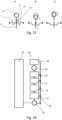
- the mechanical maximum value memory can also be designed in conjunction with a clutch (6). If the maximum value reached is stored by the locking mechanism, the rotor (8) is permanently deflected. However, if the component to be monitored then relaxes or is stressed in the opposite direction, a high force acts on the rotor (8) and thus also on the locking teeth, which could destroy the mechanism. For this reason, the maximum value memory (4) can be mechanically decoupled from the connecting element (1a, 1b) via a clutch (6).
- the clutch can consist of two opposing, mechanically separated tappets, as in Fig. 27 shown.
- One of the plungers (6.1) is attached directly to the connecting element, while the corresponding second plunger (6.2) is placed at the input of the mechanical amplifier. Displacements of the connecting element in the negative y-direction are transmitted to the second plunger via the first plunger. However, if the connecting element is deflected in the other direction, this has no effect on the second plunger and thus on the rest of the mechanism.
- the micromechanical measuring system can be used alternatively or in addition to the strain measurement for the energy-autonomous measurement of other physical quantities.
- the flexibly mounted connecting element (1a) is not connected directly to a test object (12) to be stretched, but alternatively to a mechanical Input transducer (16) designed to convert a physical quantity to be measured into a displacement or strain quantity which in turn causes a relative displacement between the frame-fixed (1b) and flexible connecting elements (1a).
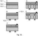
- Fig. 28 shows a possible arrangement of the individual components on the micromechanical measuring system. To restrict functions, it is conceivable that individual components could be swapped or removed. This also applies to pure strain measurement.
- Fig. 29 shows by way of example a preferred embodiment of the micromechanical measuring system in which the flexibly mounted connecting element (1a) is connected to a seismic mass (16.1) which serves as a mechanical input transducer (16) for measuring an acceleration.
- strain measuring system can be implemented using various technologies, in particular microsystem technology processes.
- SOI substrate silicon insulator
- SOI substrate silicon insulator
- These substrates comprise three layers: a so-called “device layer”, consisting made of or containing monocrystalline silicon (15.1), a buried oxide layer (BOX layer) made of SiO 2 (15.2) and a further layer made of or containing monocrystalline silicon, the buried layer (15.3).
- the device layer (15.1) carries the freely movable, two-dimensional mechanical structures such as the mechanical amplifier (2) or the maximum value memory (4), while the handle layer (15.3) can be understood as a mechanical frame that is connected to the mechanical structures of the device layer at defined locations via the SiO 2 layer of the BOX layer (15.2).
- the BOX layer (15.2) forms a sacrificial layer that is partially removed below the freely movable structures.
- both the device layer (15.1) and the handle layer (15.3) are structured. All mechanical and electromechanical components are implemented in the device layer (15.1), while the connecting elements (1a, 1b) that connect the sensor to a measurement object (12) or a flexible housing (11) are provided on the handle layer (15.3). Alternatively, the connecting elements can also be attached to the device layer.
- the handle and device layers are connected via the BOX layer (15.2), so that the mechanical displacement at the connecting elements can be transferred to the device layer.
- Fig. 30A the layer structure of the system including the electrodes (15.4) and the connecting material for the positive connection (15.5) is shown.
- Fig. 30B shows an alternative layer structure in which the handle layer (15.3) is not structured, but the device layer (15.1) is directly connected to the flexible housing (11) via the connecting material (15.5).
- Fig. 30C shows another possible arrangement in which the device layer is connected directly to the flexible housing via the connecting elements (1a, 1b, possibly 1c, 1d).
- the flexible housing (11) has a cavity in the area of the freely movable components.
- a material-locking Connection between the connecting elements (1a, 1b) and the flexible housing is also possible without connecting material, for example via anodic, eutectic or fusion bonding, provided that a suitable material such as glass or silicon is used as the substrate for the flexible housing (11).
- a solder, an adhesive and/or a stack of reactive metal layers e.g.
- the starting point for the manufacturing process is an SOI substrate or a substrate consisting of three levels, whereby the middle level (15.2) represents a sacrificial layer, the device layer level (15.1) the functional layer and the handle layer level (15.3) takes on the task of the mechanical frame (13) ( Fig. 31A ).
- a metal layer e.g. made of aluminum, is deposited on the device layer (15.1) of the wafer for electrical contact ( Fig. 31B ).
- Photolithography is then carried out, in which the desired geometry is mapped onto the device layer.
- a further etching step partially removes the previously deposited metal layer and thus structures the layer.
- the remaining photoresist on the handle layer is then removed.
- the electrodes can also be structured using a lift-off process.
- the Surfaces of the connecting elements (1a, 1b) are additionally modified, such as by deposition of a composite material (15.5) ( Fig. 31B ).
- a composite material 15.5 ( Fig. 31B ).
- an adhesion promoter or precious metal or a reactive layer stack made of e.g. Ni/Al the connection surfaces on the handle layer or the device layer are slightly modified using a lift-off process.
- the geometry of the mechanical components of the sensor is projected onto the device layer (15.1) using a further lithography process.
- the device layer (15.1) is then deep-etched through to the next layer using reactive ion deep etching ("DRIE" process) ( Fig. 31C ).
- DRIE reactive ion deep etching
- the structures on the handle layer are then etched through to the oxide layer ( Fig. 31D ).
- additional metal layers can be deposited on the deeply etched flanks of the device layer. These metal layers can be further structured using ion beam etching.
- the silicon structures are not yet freely movable up to this point.
- a hydrofluoric acid vapor or HF gas (HF vapor) process is now carried out, in which the SiO 2 layer between the handle and device layer is partially removed ( Fig. 31E ).
- Hydrofluoric acid only undercuts those structures on the device layer that are sufficiently narrow and offer a large surface area for attack. Wide structures are undercut more slowly and are therefore still firmly connected to the handle layer via the SiO 2 .
- Fig. 32 shows an alternative manufacturing process for the production of the micromechanical measuring system as well as the assembly of the measuring system on a flexible housing (11).
- Fig. 32A first shows the provision of an SOI substrate (15.1, 15.2, 15.3).
- Fig. 32B The deposition and structuring of a metal layer (15.4) is shown, which is required for the electrical connections.
- Fig. 32C After structuring the device layer (15.1) via photolithography and anisotropic etching ( Fig. 32C ) the moving structures of the micromechanical measuring system are exposed to hydrofluoric acid ( Fig. 32D).
- Fig. 32E also shows the provision a substrate (15.7) for the flexible housing.
- This substrate is preferably glass, glass ceramic, ceramic or also silicon.
- a metal layer for leading out electrodes (15.6) is also deposited and structured on the substrate (15.7) ( Fig. 32F ). Furthermore, as in Fig. 32G shown the substrate (15.7) of the flexible housing is structured by lithography and etching in such a way that cavities are created on the substrate.
- the SOI substrate and the substrate of the flexible housing are in Fig. 32H at the points of the connecting elements (1a, 1b, if necessary 1c, 1d) using a bonding process. Further connections for hermetic sealing are also possible.
- Connecting materials (15.5) such as reactive metal layers, solder or adhesive are deposited in a flat or structured manner on the surface of the flexible housing.
- manufacturing using a multi-layer structure of ceramic or metal layers is also conceivable.
- the functional layers required for the function are implemented using a ceramic or metal layer instead of silicon.
- materials can be used whose thermal expansion coefficient matches the expansion coefficient of the measurement object.
- materials such as glass ceramics (e.g. Zerodur) with particularly low thermal expansion coefficients can be used.
Landscapes
- Physics & Mathematics (AREA)
- General Physics & Mathematics (AREA)
- Measurement Of Length, Angles, Or The Like Using Electric Or Magnetic Means (AREA)
Applications Claiming Priority (2)
| Application Number | Priority Date | Filing Date | Title |
|---|---|---|---|
| DE102019131094 | 2019-11-18 | ||
| EP20208176.6A EP3822577B1 (fr) | 2019-11-18 | 2020-11-17 | Système micromécanique de mesure de déformation, procédés de fabrication et de mesure associés |
Related Parent Applications (1)
| Application Number | Title | Priority Date | Filing Date |
|---|---|---|---|
| EP20208176.6A Division EP3822577B1 (fr) | 2019-11-18 | 2020-11-17 | Système micromécanique de mesure de déformation, procédés de fabrication et de mesure associés |
Publications (2)
| Publication Number | Publication Date |
|---|---|
| EP4354082A2 true EP4354082A2 (fr) | 2024-04-17 |
| EP4354082A3 EP4354082A3 (fr) | 2024-06-12 |
Family
ID=73475883
Family Applications (3)
| Application Number | Title | Priority Date | Filing Date |
|---|---|---|---|
| EP24153205.0A Pending EP4336143A3 (fr) | 2019-11-18 | 2020-11-17 | Système de mesure micromécanique destiné à mesurer des dilatations sur un objet de mesure et à compenser une contrainte isotrope |
| EP20208176.6A Active EP3822577B1 (fr) | 2019-11-18 | 2020-11-17 | Système micromécanique de mesure de déformation, procédés de fabrication et de mesure associés |
| EP24153189.6A Pending EP4354082A3 (fr) | 2019-11-18 | 2020-11-17 | Dispositif micromécanique de mesure et de stockage autonome en énergie d'un signal de déplacement mécanique |
Family Applications Before (2)
| Application Number | Title | Priority Date | Filing Date |
|---|---|---|---|
| EP24153205.0A Pending EP4336143A3 (fr) | 2019-11-18 | 2020-11-17 | Système de mesure micromécanique destiné à mesurer des dilatations sur un objet de mesure et à compenser une contrainte isotrope |
| EP20208176.6A Active EP3822577B1 (fr) | 2019-11-18 | 2020-11-17 | Système micromécanique de mesure de déformation, procédés de fabrication et de mesure associés |
Country Status (1)
| Country | Link |
|---|---|
| EP (3) | EP4336143A3 (fr) |
Families Citing this family (8)
| Publication number | Priority date | Publication date | Assignee | Title |
|---|---|---|---|---|
| CN114295070B (zh) * | 2021-12-31 | 2024-08-20 | 澳门大学 | 长标距光纤光栅应变感测器 |
| DE102022209553B4 (de) * | 2022-09-13 | 2025-03-27 | Zf Friedrichshafen Ag | Verbindung eines auf einer Montageplatte angeordneten Sensoranordnung mit einem Messobjekt |
| DE102022209550B4 (de) * | 2022-09-13 | 2024-07-25 | Zf Friedrichshafen Ag | Verbindung eines auf einer Montageplatte angeordneten Sensoranordnung mit einem Messobjekt |
| DE102022209552B4 (de) * | 2022-09-13 | 2025-03-27 | Zf Friedrichshafen Ag | Verbindung eines auf einer Montageplatte angeordneten Sensoranordnung mit einem Messobjekt |
| CN115534921B (zh) * | 2022-11-09 | 2025-10-17 | 霍丁格必凯(苏州)电子测量技术有限公司 | 一种高铁刹车系统的数字传感器 |
| DE102023100389B3 (de) * | 2023-01-10 | 2024-05-08 | Ruhr-Universität Bochum, Körperschaft des öffentlichen Rechts | Vorrichtung und Verfahren zur energieautarken Integration eines Temperatur-Zeit-Verlaufs |
| DE102023114462B3 (de) | 2023-06-01 | 2024-11-07 | Ruhr-Universität Bochum, Körperschaft des öffentlichen Rechts | Vorrichtung und Verfahren zur Anpassung von Messbereich und Sensitivität von mikromechanischen Sensoren |
| DE102025002971A1 (de) | 2024-09-16 | 2026-03-19 | mechIC GmbH | Vorrichtung zur Dehnungsmessung und Neigungsmessung |
Citations (6)
| Publication number | Priority date | Publication date | Assignee | Title |
|---|---|---|---|---|
| DE69822097T2 (de) | 1997-11-28 | 2004-10-21 | Sarcos Inc | Dehnungsaufnehmer und dessen Verwendung |
| DE10214984B4 (de) | 2002-04-04 | 2006-01-19 | Eads Deutschland Gmbh | Aktorik- und Sensoriksystem für Verbundstrukturen |
| DE102010038062B9 (de) | 2010-10-08 | 2013-08-22 | Messphysik Materials Testing Gmbh | Ortsbestimmung und Bestimmung der Verschiebung von Orten durch berührungslose Abstandsmessung bei einer Materialprüfung |
| EP2294374B1 (fr) | 2008-06-12 | 2015-02-18 | Hottinger Baldwin Messtechnik GmbH | Capteur optique d allongement |
| DE102016202769A1 (de) | 2016-02-23 | 2017-08-24 | Technische Universität Dresden | Sensor zur integralen oder ortsaufgelösten Messung von Dehnungen basierend auf vorgeschädigten Kohlefasern |
| EP2705330B1 (fr) | 2011-04-22 | 2019-01-02 | Etat français représenté par le Délégué Général pour l'Armement | Capteur passif et réversible de déformations |
Family Cites Families (8)
| Publication number | Priority date | Publication date | Assignee | Title |
|---|---|---|---|---|
| WO2005068960A1 (fr) * | 2004-01-05 | 2005-07-28 | Case Western Reserve University | Capteurs de contrainte capacitifs |
| FR2924422B1 (fr) * | 2007-11-30 | 2009-12-25 | Commissariat Energie Atomique | Dispositif a detection par jauge de contrainte piezoresistive suspendue comportant une cellule d'amplification de contrainte. |
| FR2985721B1 (fr) * | 2012-01-12 | 2017-04-07 | Silmach | Indexation passive d'un element mobile presentant des dents |
| ITTO20130174A1 (it) * | 2013-03-05 | 2014-09-06 | St Microelectronics Srl | Dispositivo mems e relativa struttura micromeccanica con compensazione integrata delle deformazioni termo-meccaniche |
| DE102014004544A1 (de) | 2013-04-15 | 2014-10-16 | Tracto-Technik Gmbh & Co. Kg | "Gestängemagazin" |
| FR3008179B1 (fr) * | 2013-07-02 | 2015-06-12 | France Etat | Microcapteur passif et reversible de deformations |
| DE102015002452A1 (de) | 2015-02-25 | 2016-08-25 | Kiekert Aktiengesellschaft | Kraftfahrzeugschloss |
| FR3048500B1 (fr) * | 2016-03-02 | 2018-03-02 | Etat Francais Represente Par Le Delegue General Pour L'armement | Capteur de deformation permettant une discrimination de mesure en fonction de la direction de la deformation |
-
2020
- 2020-11-17 EP EP24153205.0A patent/EP4336143A3/fr active Pending
- 2020-11-17 EP EP20208176.6A patent/EP3822577B1/fr active Active
- 2020-11-17 EP EP24153189.6A patent/EP4354082A3/fr active Pending
Patent Citations (6)
| Publication number | Priority date | Publication date | Assignee | Title |
|---|---|---|---|---|
| DE69822097T2 (de) | 1997-11-28 | 2004-10-21 | Sarcos Inc | Dehnungsaufnehmer und dessen Verwendung |
| DE10214984B4 (de) | 2002-04-04 | 2006-01-19 | Eads Deutschland Gmbh | Aktorik- und Sensoriksystem für Verbundstrukturen |
| EP2294374B1 (fr) | 2008-06-12 | 2015-02-18 | Hottinger Baldwin Messtechnik GmbH | Capteur optique d allongement |
| DE102010038062B9 (de) | 2010-10-08 | 2013-08-22 | Messphysik Materials Testing Gmbh | Ortsbestimmung und Bestimmung der Verschiebung von Orten durch berührungslose Abstandsmessung bei einer Materialprüfung |
| EP2705330B1 (fr) | 2011-04-22 | 2019-01-02 | Etat français représenté par le Délégué Général pour l'Armement | Capteur passif et réversible de déformations |
| DE102016202769A1 (de) | 2016-02-23 | 2017-08-24 | Technische Universität Dresden | Sensor zur integralen oder ortsaufgelösten Messung von Dehnungen basierend auf vorgeschädigten Kohlefasern |
Non-Patent Citations (5)
| Title |
|---|
| CHEN, C ET AL.: "Femtosecond Laser-Inscribed High-Order Bragg Gratings in Large-Diameter Sapphire Fibers for High-Temperature and Strain Sensing", JOURNAL OFLIGHTWAVE TECHNOLOGY, 2018 |
| GERLACH, GW. DÖTZEL: "Fachbuchverl", CARL HANSER VERL., article "Einführung in die Mikrosystemtechnik ein Kursbuch für Studierende 2006", pages: 384 |
| SCHOMBURG, W.K.: "Introduction to Microsystem Design", 2011, SPRINGER |
| TIAN, Q. H.YAN, L. P.YANG, T.CHEN, B. Y: "In Applied Mechanics and Materials", vol. 117, 2012, TRANS TECH PUBLICATIONS, article "Recent Developments of Material Deformation Measurement", pages: 122 - 128 |
| TIETZE, U.C. SCHENKE. GAMM: "Halbleiter-Schaltungstechnik", 2012, SPRINGER-VERLAG |
Also Published As
| Publication number | Publication date |
|---|---|
| EP4336143A2 (fr) | 2024-03-13 |
| EP3822577B1 (fr) | 2024-01-24 |
| EP4336143A3 (fr) | 2024-05-15 |
| EP3822577A1 (fr) | 2021-05-19 |
| EP4354082A3 (fr) | 2024-06-12 |
Similar Documents
| Publication | Publication Date | Title |
|---|---|---|
| EP3822577B1 (fr) | Système micromécanique de mesure de déformation, procédés de fabrication et de mesure associés | |
| EP3870930B1 (fr) | Structure de mesure de dilatation dotée d'un support structuré | |
| EP2013598B1 (fr) | Dispositif de mesure de force pour mesurer la force dans le cas d'actionneurs monolithiques, procédé de mesure d'une force et utilisation du dispositif de mesure de force | |
| Ştefănescu | Handbook of Force Transducers: Characteristics and Applications | |
| EP4302059B1 (fr) | Dispositif de mesure de déformations, de contraintes, de forces et/ou de couples dans une pluralité d'axes | |
| DE19647876A1 (de) | Sensor zur Messung von mechanischen Kräften | |
| WO2006072391A1 (fr) | Dispositif de mesure de force, en particulier capteur de pression, et son procédé de production | |
| WO2011015302A1 (fr) | Ensemble et procédé pour la mesure de pression capacitive | |
| EP1612531A2 (fr) | Structure micromécanique | |
| Shokuhfar et al. | Low-cost polymeric microcantilever sensor with titanium as piezoresistive material | |
| DE102006058882B4 (de) | Separate Erfassung von Zuspann- und Reibkräften an einer Bremse | |
| WO2008040656A2 (fr) | Détecteur à microsystème électromécanique (mems) pour environnements extrêmes | |
| DE102010054970A1 (de) | Vorrichtung zum Wandeln einer Dehnung und/oder Stauchung in ein elektrisches Signal, insbesondere Dehnungsmessfolie | |
| DE102023100389B3 (de) | Vorrichtung und Verfahren zur energieautarken Integration eines Temperatur-Zeit-Verlaufs | |
| DE102008063797B4 (de) | Messgerät | |
| EP1952089A1 (fr) | Mesure de tension de revêtements avec un activateur piézoélectrique | |
| DE69425898T2 (de) | Hochpräzisionswaage und positionssensor | |
| DE4309530A1 (de) | Vorrichtung für die dynamisch-mechanische Analyse | |
| EP4481345B1 (fr) | Dispositif et procédé d'adaptation de plage de mesure et de sensibilité de capteurs micromécaniques | |
| DE102011006922B4 (de) | Messwandler für die Sensortechnik | |
| DE19857124C2 (de) | Kraftsensor-System | |
| DE102010017191B4 (de) | Differenzdrucksensor mit Absolutdruckermittlung | |
| DE102025002971A1 (de) | Vorrichtung zur Dehnungsmessung und Neigungsmessung | |
| DE19915288A1 (de) | Vorrichtung zur Untersuchung von Reibverhältnissen | |
| Subramanya et al. | MEMS and MEMS based strain gauge load cells—A review |
Legal Events
| Date | Code | Title | Description |
|---|---|---|---|
| PUAI | Public reference made under article 153(3) epc to a published international application that has entered the european phase |
Free format text: ORIGINAL CODE: 0009012 |
|
| STAA | Information on the status of an ep patent application or granted ep patent |
Free format text: STATUS: THE APPLICATION HAS BEEN PUBLISHED |
|
| AC | Divisional application: reference to earlier application |
Ref document number: 3822577 Country of ref document: EP Kind code of ref document: P |
|
| AK | Designated contracting states |
Kind code of ref document: A2 Designated state(s): AL AT BE BG CH CY CZ DE DK EE ES FI FR GB GR HR HU IE IS IT LI LT LU LV MC MK MT NL NO PL PT RO RS SE SI SK SM TR |
|
| REG | Reference to a national code |
Ref country code: DE Ref legal event code: R079 Free format text: PREVIOUS MAIN CLASS: G01B0021320000 Ipc: G01B0005000000 |
|
| PUAL | Search report despatched |
Free format text: ORIGINAL CODE: 0009013 |
|
| AK | Designated contracting states |
Kind code of ref document: A3 Designated state(s): AL AT BE BG CH CY CZ DE DK EE ES FI FR GB GR HR HU IE IS IT LI LT LU LV MC MK MT NL NO PL PT RO RS SE SI SK SM TR |
|
| RIC1 | Information provided on ipc code assigned before grant |
Ipc: G06M 1/27 20060101ALI20240506BHEP Ipc: G06M 1/08 20060101ALI20240506BHEP Ipc: G01B 21/32 20060101ALI20240506BHEP Ipc: G01B 7/16 20060101ALI20240506BHEP Ipc: G01B 5/30 20060101ALI20240506BHEP Ipc: G01B 5/00 20060101AFI20240506BHEP |
|
| STAA | Information on the status of an ep patent application or granted ep patent |
Free format text: STATUS: REQUEST FOR EXAMINATION WAS MADE |
|
| 17P | Request for examination filed |
Effective date: 20241210 |
|
| STAA | Information on the status of an ep patent application or granted ep patent |
Free format text: STATUS: EXAMINATION IS IN PROGRESS |
|
| 17Q | First examination report despatched |
Effective date: 20260212 |