EP4354155A1 - Appareil d'échantillonnage de tension et procédé associé - Google Patents
Appareil d'échantillonnage de tension et procédé associé Download PDFInfo
- Publication number
- EP4354155A1 EP4354155A1 EP21950511.2A EP21950511A EP4354155A1 EP 4354155 A1 EP4354155 A1 EP 4354155A1 EP 21950511 A EP21950511 A EP 21950511A EP 4354155 A1 EP4354155 A1 EP 4354155A1
- Authority
- EP
- European Patent Office
- Prior art keywords
- signal
- voltage division
- voltage
- differential
- switch
- Prior art date
- Legal status (The legal status is an assumption and is not a legal conclusion. Google has not performed a legal analysis and makes no representation as to the accuracy of the status listed.)
- Pending
Links
Images











Classifications
-
- G—PHYSICS
- G01—MEASURING; TESTING
- G01R—MEASURING ELECTRIC VARIABLES; MEASURING MAGNETIC VARIABLES
- G01R15/00—Details of measuring arrangements of the types provided for in groups G01R17/00 - G01R29/00, G01R33/00 - G01R33/26 or G01R35/00
- G01R15/04—Voltage dividers
-
- G—PHYSICS
- G01—MEASURING; TESTING
- G01R—MEASURING ELECTRIC VARIABLES; MEASURING MAGNETIC VARIABLES
- G01R19/00—Arrangements for measuring currents or voltages or for indicating presence or sign thereof
- G01R19/0084—Measuring voltage only
-
- G—PHYSICS
- G01—MEASURING; TESTING
- G01R—MEASURING ELECTRIC VARIABLES; MEASURING MAGNETIC VARIABLES
- G01R35/00—Testing or calibrating of apparatus covered by the other groups of this subclass
- G01R35/005—Calibrating; Standards or reference devices, e.g. voltage or resistance standards, "golden" references
Definitions
- This application relates to the field of power electronics technologies, and in particular, to a voltage sampling apparatus and a related method.
- the analog-to-digital conversion technology as an interface between an analog technology and a digital technology, is a technology of converting a voltage signal obtained through sampling into a digital signal, and is increasingly concerned by various circles, and application scenarios of the analog-to-digital conversion technology are more diversified. To meet high performance requirements in various application scenarios, people have increasingly high requirements on voltage signal sampling.
- common multi-channel voltage signal sampling technologies include two types: One is an isolation sampling technology in which a voltage signal sampled by each channel is input to a sampling chip.
- a signal processing circuit, a signal isolation circuit, an isolation circuit, and the like need to be added to process the voltage signal before the voltage signal is sent to the sampling chip.
- the other is a resistor voltage division differential sampling technology in which after a voltage division of each high-end voltage is reduced, a differential voltage is sent to a sampling chip.
- a differential resistor element needs to be selected according to the withstand voltage limitation condition of the sampling chip, to obtain a resistor voltage division ratio that meets a requirement.
- isolation sampling technology because multiple circuit modules need to be added to process a voltage signal, a problem of increasing costs of the isolation sampling technology is caused, and batch production is not facilitated.
- resistor voltage division differential sampling technology due to a manufacturing process of a resistor element or other environmental factors, a problem of an electrical characteristic deviation of the resistor element is caused, and voltage signal sampling precision is reduced.
- Embodiments of the present invention provide a voltage sampling apparatus and a related method, to provide a more simplified voltage sampling apparatus with higher sampling precision.
- an embodiment of the present invention provides a voltage sampling apparatus.
- the voltage sampling apparatus includes a differential circuit, a voltage division circuit, and a first calibration switch.
- the voltage division circuit includes a first voltage division branch and a second voltage division branch. A first output end of the differential circuit and an input end of the first voltage division branch are connected to a first end of the first calibration switch. A second output end of the differential circuit and an input end of the second voltage division branch are connected to a second end of the first calibration switch.
- the differential circuit When the first calibration switch is in an on state, the differential circuit is configured to: input a target signal to the first voltage division branch and the second voltage division branch that are connected in parallel, where the target signal is a first differential output signal output by the first output end or a second differential output signal output by the second output end.
- the voltage division circuit is configured to: receive the target signal by using the first voltage division branch and perform voltage division according to a first voltage division ratio k 1 to output a first voltage signal, and receive the target signal by using the second voltage division branch and perform voltage division according to a second voltage division ratio k 2 to output a second voltage signal, where a difference between the first voltage signal and the second voltage signal is a first deviation signal, and the first deviation signal is used to calibrate a difference between the first voltage division ratio and the second voltage division ratio.
- a differential sampling signal of the differential circuit is obtained (it should be emphasized that, to facilitate restoration, based on the sampled voltage signals, of the difference between the voltage signals actually output by the differential circuit, voltage division usually needs to be performed on the two voltage division branches according to the same ratio).
- the voltage signal provided by the differential circuit usually needs to be reduced in a voltage division manner according to a specific ratio.
- the voltage signal output by one end of the differential circuit is divided by using the first voltage division branch according to a voltage division ratio, and the voltage signal output by the other end of the differential circuit is divided by using the second voltage division branch according to a same voltage division ratio.
- the sampling chip can bear a voltage signal that is reduced by ratio by a voltage division branch.
- the voltage division branch provides a voltage signal reduction function
- capabilities namely, voltage division capabilities
- the difference between the voltage signals actually provided by the differential circuit cannot be accurately restored according to a theoretical voltage division ratio based on the voltage signal sampled by the sampling chip.
- a sampling result is inaccurate, and sampling precision is low.
- the first calibration switch is added based on a conventional technology, and the first calibration switch controls a connection status of the first voltage division branch and the second voltage division branch.
- the voltage sampling apparatus is in a calibration state, to calibrate the difference between the voltage division ratio of the first voltage division branch and the voltage division ratio of the second voltage division branch. This improves sampling precision of the voltage sampling apparatus.
- the first voltage division branch in the voltage sampling apparatus includes a plurality of series-connected resistors (for example, R1 and R2)
- the second voltage division branch includes a plurality of series-connected resistors (for example, R3 and R4)
- the voltage division ratio of the first voltage division branch is the same as that of the second voltage division branch. In other words, theoretically the difference between k 1 and k 2 is 0.
- there is a specific error between a theoretical resistance value and an actual resistance value of the resistor in each voltage division branch there is an error between a theoretical value and an actual value of k 1
- the first calibration switch is switched on, so that the first voltage division branch and the second voltage division branch are in a parallel-connected state, and the first voltage division branch and the second voltage division branch separately receive a target signal U target (the first differential output signal or the second differential output signal) output by the differential circuit, so that the difference (the first deviation signal) of the voltage signals output by the voltage division circuit can be actually measured, where the first deviation signal may indicate a deviation between the voltage division capabilities of the two voltage division branches. Therefore, the deviation is superimposed on one of the voltage division branches, so that the voltage division capabilities of the two voltage division branches are equal.
- sampling precision originally determined by superimposing two error factors (a first voltage division ratio error and a second voltage division ratio error) is converted into sampling precision determined by one error factor (the first voltage division ratio error or the second voltage division ratio error). That is, the error factor is reduced. Subsequently, only one error factor is used for calibration, so that sampling precision can be improved.
- an error of the difference between the voltage division ratios provided by the two voltage division branches can be calibrated, so that the voltage division capability of the first voltage division branch is the same as the voltage division capability of the second voltage division branch. This effectively eliminates a sampling error caused by inconsistent voltage division capabilities of the two voltage division branches, and improves sampling precision.
- the first voltage division branch and the second voltage division branch are switched from a parallel-connected state to an open-circuit state.
- the differential circuit is further configured to: input the first differential output signal to the first voltage division branch through the first output end, and input the second differential output signal to the second voltage division branch through the second output end.
- the voltage division circuit is further configured to: receive the first differential output signal by using the first voltage division branch and perform voltage division according to k 1 to output a third voltage signal, and receive the second differential output signal by using the second voltage division branch and perform voltage division according to k 2 to output a fourth voltage signal, where a difference between the third voltage signal and the fourth voltage signal is a first sampling signal.
- the voltage sampling apparatus when the first calibration switch is switched from the on state to the off state, the voltage sampling apparatus enters a sampling state, the first voltage division branch and the second voltage division branch in the voltage division circuit are switched from the parallel-connected state to the open-circuit state, and the first voltage division branch and the second voltage division branch respectively receive the different voltage signals and perform voltage division according to the respective voltage division ratios, to output a voltage signal that can be borne by the sampling chip.
- the first voltage division branch receives the voltage signal output by one end of the differential circuit
- the second voltage division branch receives the voltage signal output by the other end of the differential circuit.
- the two voltage division branches respectively perform voltage division on the two voltage signals according to the respective voltage division ratios, and determine a difference between the two voltage signals obtained through voltage division as a first differential sampling signal.
- the voltage sampling apparatus further includes a calibration module.
- the calibration module is configured to: obtain a second sampling signal through calculation based on the first deviation signal and the first sampling signal, where the second sampling signal indicates a difference between voltage signals obtained after voltage division is performed on the first differential output signal and the second differential output signal according to a same voltage division ratio, and the same voltage division ratio is the first voltage division ratio or the second voltage division ratio; and when the target signal is the first differential output signal, restore, according to kz, the second sampling signal as a sampling value of a difference between the first differential output signal and the second differential output signal; or when the target signal is the second differential output signal, restore, according to ki, the second sampling signal as a sampling value of a difference between the first differential output signal and the second differential output signal.
- the calibration module may remove, based on the first sampling signal, the foregoing first deviation signal (namely, a sampling error caused by inconsistent voltage division capabilities of the two voltage division branches) to obtain the second sampling signal, so that the sampling error caused by the inconsistent voltage division capabilities of the two voltage division branches is effectively eliminated.
- the sampling precision originally determined by superimposing the two error factors namely, the first voltage division ratio error and the second voltage division ratio error
- the sampling precision is converted into the sampling precision determined by one error factor (namely, the first voltage division ratio error or the second voltage division ratio error).
- the error factor is reduced.
- the second sampling signal is restored, according to the theoretical voltage division ratio, as a sampling value of the difference between the two voltage signals actually output by the differential circuit. This avoids the sampling error caused by the inconsistent voltage division capabilities of the two voltage division branches, and improves sampling precision.
- U sampling1 indicates the first sampling signal
- U difference1 indicates the first differential output signal
- U difference2 indicates the second differential output signal
- U difference1 (k 1 -k 2 ) and U difference2 (k 1 -k 2 ) indicate the first deviation signal
- the foregoing first deviation signal namely, the sampling error caused by the inconsistent voltage division capabilities of the two voltage division branches
- the sampling precision originally determined by superimposing the two error factors namely, the first voltage division ratio error and the second voltage division ratio error
- the sampling precision is converted into the sampling precision determined by one error factor (namely, the first voltage division ratio error or the second voltage division ratio error).
- the error factor is reduced.
- the second sampling signal is restored, according to the theoretical voltage division ratio, as the sampling value of the difference between the two voltage signals actually output by the differential circuit. This avoids the sampling error caused by the inconsistent voltage division capabilities of the two voltage division branches, and improves sampling precision.
- the first switch group and the second switch group may be designed in the differential circuit.
- the first switch group may be configured to control a voltage signal flow direction of an odd-numbered cell
- the second switch group may be configured to control a voltage signal flow direction of an even-numbered cell.
- the first calibration switch is in an on state; and when the i th first switch is in an on state and the i th second switch is in an off state, the differential circuit is specifically configured to: receive a first differential input signal output by the (2i-1) th cell, and input, by using the i th first switch that is switched on, the first differential output signal to the first voltage division branch and the second voltage division branch that are connected in parallel; or when the i th first switch is in an off state and the i th second switch is in an on state, the differential circuit is specifically configured to: receive a second differential input signal output by the 2i th cell, and input, by using the i th second switch that is switched on, the second differential output signal to the first voltage division branch and the second voltage division branch that are connected in parallel.
- the voltage sampling apparatus when the first calibration switch is switched on, the voltage sampling apparatus is in a voltage signal calibration stage.
- the first voltage division branch and the second voltage division branch receive only one same voltage signal. Therefore, the i th first switch may be switched on, and the i th second switch may be switched off, to ensure that only a voltage signal of the (2i-1) th cell is input to the differential circuit, and the differential circuit outputs only the first differential output signal.
- the i th second switch may be switched on, and the i th first switch may be switched off, to ensure that only a voltage signal of the 2i th cell is input to the differential circuit, and the differential circuit outputs only the second differential output signal.
- the deviation signal is obtained based on the first differential output signal or the deviation signal is obtained based on the second differential output signal. This can effectively eliminate the sampling error caused by the inconsistent voltage division capabilities of the two voltage division branches, and improves sampling precision based on the deviation signal.
- the first calibration switch is in an off state; and when both the i th first switch and the i th second switch are in an on state, the differential circuit is specifically configured to: receive a first differential input signal output by the (2i-1) th cell and input the first differential output signal to the first voltage division branch by using the i th first switch that is switched on, and receive a second differential input signal output by the 2i th cell and input the second differential output signal to the second voltage division branch by using the i th second switch that is switched on.
- the voltage sampling apparatus when the first calibration switch is switched off, the voltage sampling apparatus is in a voltage signal sampling stage.
- the first voltage division branch and the second voltage division branch need to receive two different voltage signals. Therefore, the i th first switch and the i th second switch may be switched on, to ensure that the differential circuit can separately receive voltage signals of the (2i-1) th cell and the 2i th cell, and the differential circuit can separately output two voltage signals (obtained based on the voltage signals of the (2i-1) th cell and the 2i th cell).
- the voltage sampling apparatus further includes a second calibration switch; one end of the second calibration switch is connected to the first end of the first calibration switch, and the other end is connected to a reference power supply; and when both the i th first switch and the i th second switch are in an off state, and the first calibration switch and the second calibration switch are in an on state, the voltage division circuit is further configured to: receive, by using the second voltage division branch, a reference voltage signal output by the reference power supply, and perform voltage division according to k 2 to output a fifth voltage signal, where the fifth voltage signal is used to calibrate k 2 .
- the sampling precision originally determined by superimposing the two error factors (the first voltage division ratio error and the second voltage division ratio error) is converted into the sampling precision determined by one error factor (the first voltage division ratio error or the second voltage division ratio error). Further, to avoid impact of the only error factor on sampling, a difference that is closer to the difference between the two voltage signals actually output by the differential circuit is obtained.
- the second calibration switch is added to the voltage sampling apparatus, is externally connected to the reference power supply, and is configured to calibrate a voltage division ratio of each voltage division branch in the voltage division circuit.
- the second voltage division branch in the voltage division circuit can receive the voltage signal output by the reference power supply, and then the second voltage division branch performs voltage division on the voltage signal and outputs the fifth voltage signal, so that a value of the fifth voltage signal can be actually measured.
- the reference power supply can output a stable and known voltage signal. Therefore, the voltage division ratio of the second voltage division branch may be obtained based on the actually measured value of the fifth voltage signal and a value of the voltage signal of the reference power supply, to calibrate the voltage division ratio of the second voltage division branch.
- the calibration module is specifically configured to: when the target signal is the first differential output signal, restore, according to the calibrated kz, the second sampling signal as the sampling value of the difference between the first differential output signal and the second differential output signal.
- the second sampling signal is restored, according to the calibrated second voltage division ratio, as the sampling value of the difference between the two voltage signals actually output by the differential circuit. This avoids a sampling error caused to sampling by the voltage division ratio, and further improves sampling precision of the voltage sampling apparatus.
- the voltage division circuit is further configured to: receive, by using the first voltage division branch, the reference voltage signal output by the reference power supply, and perform voltage division according to k 1 to output a sixth voltage signal, where the sixth voltage signal is used to calibrate k 1 .
- the first voltage division branch in the voltage division circuit can receive the voltage signal output by the reference power supply, and then the first voltage division branch performs voltage division on the voltage signal and outputs the sixth voltage signal, so that a value of the sixth voltage signal can be actually measured.
- the reference power supply can output a stable and known voltage signal. Therefore, the voltage division ratio of the first voltage division branch may be obtained based on the actually measured value of the sixth voltage signal and the value of the voltage signal of the reference power supply, to calibrate the voltage division ratio of the first voltage division branch.
- the calibration module is specifically configured to: when the target signal is the second differential output signal, restore, according to the calibrated ki, the second sampling signal as the sampling value of the difference between the first differential output signal and the second differential output signal.
- the second sampling signal is restored, according to the calibrated first voltage division ratio, as the sampling value of the difference between the two voltage signals actually output by the differential circuit. This avoids the sampling error caused to sampling by the voltage division ratio, and further improves sampling precision of the voltage sampling apparatus.
- a ground end of the first voltage division branch and a ground end of the second voltage division branch are both connected to a ground cable.
- the first voltage division branch includes M series-connected first voltage division resistors
- the second voltage division branch includes M series-connected second voltage division resistors
- M is an integer greater than 1.
- the voltage division circuit is specifically configured to: perform, by using the M series-connected first voltage division resistors, voltage division on the target signal according to k 1 to output the first voltage signal, and perform, by using the M series-connected second voltage division resistors, voltage division on the target signal according to k 2 to output the second voltage signal.
- a voltage division element may be a plurality of series-connected resistors, to implement voltage division on an input voltage signal, to output a voltage signal that meets a voltage withstand limitation condition of the sampling chip.
- the first voltage division branch and the second voltage division branch separately perform voltage division on the target signal (the first differential output signal or the second differential output signal) by using respective voltage division resistors, to output two voltage signals obtained through voltage division.
- the voltage division circuit when the first calibration switch is in an off state, is specifically configured to: perform, by using the M series-connected first voltage division resistors, voltage division on the first differential output signal according to k 1 to output the third voltage signal, and perform, by using the M series-connected second voltage division resistors, voltage division on the second differential output signal according to k 2 to output the fourth voltage signal.
- the first voltage division branch receives the first differential output signal, and performs voltage division on the signal by using the voltage division resistors, to output the voltage signal obtained through voltage division.
- the second voltage division branch receives the second differential output signal, and performs voltage division on the signal by using the voltage division resistors, to output the voltage signal obtained through voltage division.
- the voltage sampling apparatus further includes an analog-to-digital converter.
- the analog-to-digital converter is configured to: receive an output signal of the voltage division circuit, and convert the output signal from an analog signal into a digital signal, where the output signal includes the first voltage signal and the second voltage signal, or the third voltage signal and the fourth voltage signal, or the fifth voltage signal, or the sixth voltage signal.
- the voltage sampling apparatus may further include the analog-to-digital converter.
- the analog-to-digital converter can directly convert an analog signal output by the voltage division circuit into a digital signal, to facilitate subsequent digital operation.
- an embodiment of the present invention provides a voltage sampling method, applied to a voltage sampling apparatus.
- the voltage sampling apparatus includes a differential circuit, a voltage division circuit, and a first calibration switch.
- the voltage division circuit includes a first voltage division branch and a second voltage division branch. A first output end of the differential circuit and an input end of the first voltage division branch are connected to a first end of the first calibration switch. A second output end of the differential circuit and an input end of the second voltage division branch are connected to a second end of the first calibration switch.
- the method includes: when the first calibration switch is in an on state, inputting, by using the differential circuit, a target signal to the first voltage division branch and the second voltage division branch that are connected in parallel, where the target signal is a first differential output signal output by the first output end or a second differential output signal output by the second output end; receiving the target signal by using the first voltage division branch of the voltage division circuit and performing voltage division according to a first voltage division ratio k 1 to output a first voltage signal, and receiving the target signal by using the second voltage division branch and performing voltage division according to a second voltage division ratio k 2 to output a second voltage signal, where a difference between the first voltage signal and the second voltage signal is a first deviation signal, and the first deviation signal is used to calibrate a difference between the first voltage division ratio and the second voltage division ratio.
- the first voltage division branch and the second voltage division branch are switched from a parallel-connected state to an open-circuit state.
- the method further includes: inputting the first differential output signal to the first voltage division branch through the first output end of the differential circuit, and inputting the second differential output signal to the second voltage division branch through the second output end; and receiving the first differential output signal by using the first voltage division branch of the voltage division circuit and performing voltage division according to k 1 to output a third voltage signal, and receiving the second differential output signal by using the second voltage division branch and performing voltage division according to k 2 to output a fourth voltage signal, where a difference between the third voltage signal and the fourth voltage signal is a first sampling signal.
- the voltage sampling apparatus further includes a calibration module.
- the method further includes: obtaining, by using the calibration module, a second sampling signal through calculation based on the first deviation signal and the first sampling signal, where the second sampling signal indicates a difference between voltage signals obtained after voltage division is performed on the first differential output signal and the second differential output signal according to a same voltage division ratio, and the same voltage division ratio is the first voltage division ratio or the second voltage division ratio; and when the target signal is the first differential output signal, restoring, by using the calibration module according to kz, the second sampling signal as a sampling value of a difference between the first differential output signal and the second differential output signal; or when the target signal is the second differential output signal, restoring, by using the calibration module according to ki, the second sampling signal as a sampling value of a difference between the first differential output signal and the second differential output signal.
- the first calibration switch is in an on state.
- the inputting, by using the differential circuit, a target signal to the first voltage division branch and the second voltage division branch that are connected in parallel includes: when the i th first switch is in an on state and the i th second switch is in an off state, receiving, by using the differential circuit, a first differential input signal output by the (2i-1) th cell, and inputting, by using the i th first switch that is switched on, the first differential output signal to the first voltage division branch and the second voltage division branch that are connected in parallel; or when the i th first switch is in an off state and the i th second switch is in an on state, receiving, by using the differential circuit, a second differential input signal output by the 2i th cell, and inputting, by using the i th second switch that is switched on, the second differential output signal to the first voltage division branch and the second voltage division branch that are connected in parallel.
- the first calibration switch is in an off state.
- the inputting the first differential output signal to the first voltage division branch through the first output end of the differential circuit, and inputting the second differential output signal to the second voltage division branch through the second output end includes: when both the i th first switch and the i th second switch are in an on state, receiving, by using the differential circuit, a first differential input signal output by the (2i-1) th cell and inputting the first differential output signal to the first voltage division branch by using the i th first switch that is switched on, and receiving a second differential input signal output by the 2i th cell and inputting the second differential output signal to the second voltage division branch by using the i th second switch that is switched on.
- the voltage sampling apparatus further includes a second calibration switch.
- One end of the second calibration switch is connected to the first end of the first calibration switch, and the other end is connected to a reference power supply.
- the method further includes: receiving, by using the second voltage division branch of the voltage division circuit, a reference voltage signal output by the reference power supply, and performing voltage division according to k 2 to output a fifth voltage signal, where the fifth voltage signal is used to calibrate k 2 .
- the restoring, according to kz, the second sampling signal as a sampling value of a difference between the first differential output signal and the second differential output signal when the target signal is the first differential output signal includes: when the target signal is the first differential output signal, restoring, by using the calibration module according to the calibrated kz, the second sampling signal as the sampling value of the difference between the first differential output signal and the second differential output signal.
- the method further includes: receiving, by using the first voltage division branch of the voltage division circuit, the reference voltage signal output by the reference power supply, and performing voltage division according to k 1 to output a sixth voltage signal, where the sixth voltage signal is used to calibrate k 1 .
- the restoring, according to ki, the second sampling signal as a sampling value of a difference between the first differential output signal and the second differential output signal when the target signal is the second differential output signal includes: when the target signal is the second differential output signal, restoring, by using the calibration module according to the calibrated ki, the second sampling signal as the sampling value of the difference between the first differential output signal and the second differential output signal.
- a ground end of the first voltage division branch and a ground end of the second voltage division branch are both connected to a ground cable.
- the first voltage division branch includes M series-connected first voltage division resistors
- the second voltage division branch includes M series-connected second voltage division resistors
- M is an integer greater than 1.
- the receiving the target signal by using the first voltage division branch of the voltage division circuit and performing voltage division to output a first voltage signal, and receiving the target signal by using the second voltage division branch and performing voltage division to output a second voltage signal includes: performing, by using the M series-connected first voltage division resistors of the voltage division circuit, voltage division on the target signal according to k 1 to output the first voltage signal, and performing, by using the M series-connected second voltage division resistors, voltage division on the target signal according to k 2 to output the second voltage signal.
- the receiving the first differential output signal by using the first voltage division branch of the voltage division circuit and performing voltage division to output a third voltage signal, and receiving the second differential output signal by using the second voltage division branch and performing voltage division to output a fourth voltage signal includes: performing, by using the M series-connected first voltage division resistors of the voltage division circuit, voltage division on the first differential output signal according to k 1 to output the third voltage signal, and performing, by using the M series-connected second voltage division resistors, voltage division on the second differential output signal according to k 2 to output the fourth voltage signal.
- the voltage sampling apparatus further includes an analog-to-digital converter.
- the method further includes: receiving, by using the analog-to-digital converter, an output signal of the voltage division circuit, and converting the output signal from an analog signal into a digital signal, where the output signal includes the first voltage signal and the second voltage signal, or the third voltage signal and the fourth voltage signal, or the fifth voltage signal, or the sixth voltage signal.
- this application provides a terminal device.
- the terminal device has a function of implementing the method according to any one of the foregoing voltage sampling method embodiments.
- the function may be implemented by hardware, or may be implemented by hardware executing corresponding software.
- the hardware or the software includes one or more modules corresponding to the function.
- this application provides a terminal device.
- the terminal device includes a processor.
- the processor is configured to support the terminal device in performing a corresponding function in the voltage sampling method provided in the second aspect.
- the terminal device may further include a memory.
- the memory is coupled to the processor, and stores program instructions and data that are necessary for the terminal device.
- the terminal device may further include a communication interface, configured to implement communication between the terminal device and another device or a communication network.
- an embodiment of the present invention provides a computer program.
- the computer program includes instructions.
- the computer program is executed by a computer, the computer is enabled to perform a procedure in the voltage sampling method according to any one of the implementations of the second aspect.
- this application provides a chip system.
- the chip system includes a processor, configured to support an application server or a terminal device in implementing a function in the foregoing aspects, for example, generating or processing information in the foregoing methods.
- the chip system further includes a memory.
- the memory is configured to store program instructions and data that are necessary for a data sending device.
- the chip system may include a chip, or may include a chip and another discrete component.
- this application provides a semiconductor chip.
- the semiconductor chip includes the voltage sampling apparatus according to any one of the implementations of the first aspect.
- this application provides an electronic device.
- the electronic device includes the semiconductor chip according to the seventh aspect.
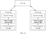
- FIG. 1A is a schematic diagram of a system architecture of an application scenario of a voltage sampling apparatus according to an embodiment of the present invention.
- the system architecture includes at least one server 10 and one or more terminals 20 (two terminals are used as an example in the figure).
- the server 10 generates a preset algorithm for analyzing a voltage signal.
- the terminal 20 may include a voltage sampling apparatus 201, N series-connected cells 202, and an operation unit 203 in this application.
- the operation unit 203 may analyze, according to the preset algorithm provided by the server 10, voltage signals that are of the N series-connected cells 202 and that are collected by the voltage sampling apparatus 201, to predict power supply capabilities of the N series-connected cells 202 or perform battery management.
- the terminal 20 in the system architecture may be specifically at least one of a battery-powered device such as a smartphone, a communication base station, a data center, a photovoltaic inverter, or an electric vehicle.
- the battery-powered device includes at least one battery product.
- the battery product includes the N series-connected cells 202 and the voltage sampling apparatus 201.
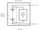
- FIG. 1B is a schematic diagram of a battery product according to an embodiment of the present invention.
- the N series-connected cells 202 of the battery product are used as a power supply system.
- the voltage sampling apparatus 201 is connected to the N series-connected cells 202, and is configured to collect voltage signals of the N series-connected cells 202.
- the server 10 pre-installs firmware in batches on another terminal 20 of a same model as the terminal.
- the firmware may include a preset algorithm for analyzing a voltage signal.
- the preset algorithm may be stored in an internal storage unit of the terminal 20, for example, a read-only memory (Read-Only Memory, ROM), namely, a default place in which system firmware and software of the terminal 20 are installed.
- ROM Read-Only Memory
- the firmware including the preset algorithm cannot be randomly read or written.
- the voltage sampling apparatus 201 in this application may periodically collect a voltage signal of each individual cell of the N series-connected cells 202, and analyze and manage the sampled voltage signals by using the operation unit 203 according to the preset algorithm, so that a voltage deviation of a single cell can be kept within an expected range. This ensures that each individual cell is not damaged during proper use, and ensures safety and stability of the N series-connected cells 202.
- system architecture corresponding to the foregoing application scenario is merely several example implementations in embodiments of the present invention.
- the application scenario and the corresponding system architecture in embodiments of the present invention include but are not limited to the foregoing descriptions.
- FIG. 2A is a schematic diagram of a voltage sampling apparatus according to an embodiment of the present invention.
- the voltage sampling apparatus 30 includes a differential circuit 301, a voltage division circuit 302, and a first calibration switch 303.
- the voltage division circuit 302 includes a first voltage division branch 3021 and a second voltage division branch 3022.
- a first output end 3011 of the differential circuit 301 and an input end of the first voltage division branch 3021 are connected to a first end 3031 of the first calibration switch 303.
- a second output end 3012 of the differential circuit 301 and an input end of the second voltage division branch 3022 are connected to a second end 3032 of the first calibration switch 303.
- FIG. 2B is a schematic diagram of a voltage signal calibration process according to an embodiment of the present invention. As shown in FIG. 2B , when the first calibration switch 303 is in an on state, the first voltage division branch 3021 and the second voltage division branch 3022 are in a parallel-connected state.
- the differential circuit 301 has two signal output ends, there are two methods for outputting a target signal.
- a first method as shown in (a) in FIG. 2B , the differential circuit 301 outputs a first differential output signal as a target signal through the first output end 3011 and separately inputs the first differential output signal to the first voltage division branch 3021 and the second voltage division branch 3022.
- a second method as shown in (b) in FIG.
- the differential circuit 301 outputs a second differential output signal as a target signal through the second output end 3012 and separately inputs the second differential output signal to the first voltage division branch 3021 and the second voltage division branch 3022. It may be understood that different output ends of the differential circuit 301 output different voltage signals. Therefore, the target signal is the first differential output signal output by the first output end 3011, or the second differential output signal output by the second output end 3012.
- the voltage division circuit 302 is configured to: receive the target signal by using the first voltage division branch 3021 and perform voltage division according to a first voltage division ratio k 1 to output a first voltage signal, and receive the target signal by using the second voltage division branch 3022 and perform voltage division according to a second voltage division ratio k 2 to output a second voltage signal, where a difference between the first voltage signal and the second voltage signal is a first deviation signal, and the first deviation signal is used to calibrate a difference between the first voltage division ratio and the second voltage division ratio.
- a difference between the first voltage signal and the second voltage signal is a first deviation signal
- the first deviation signal is used to calibrate a difference between the first voltage division ratio and the second voltage division ratio.
- the first voltage division branch 3021 of the voltage division circuit 302 receives the first differential output signal (the target signal) output by the first output end 3011, and performs voltage division on the signal by using a voltage division element in the first voltage division branch 3021 according to the first voltage division ratio to output the first voltage signal.
- the second voltage division branch 3022 of the voltage division circuit 302 receives the first differential output signal output by the first output end 3011, and performs voltage division on the signal by using a voltage division element in the second voltage division branch 3022 according to the second voltage division ratio to output the second voltage signal.
- the first voltage division branch 3021 of the voltage division circuit 302 receives the second differential output signal (the target signal) output by the second output end 3012, and performs voltage division on the signal by using a voltage division element in the first voltage division branch 3021 according to the first voltage division ratio to output the first voltage signal.
- the second voltage division branch 3022 of the voltage division circuit 302 receives the second differential output signal output by the second output end 3012, and performs voltage division on the signal by using a voltage division element in the second voltage division branch 3022 according to the second voltage division ratio to output the second voltage signal.
- the first deviation signal is obtained based on the first voltage signal and the second voltage signal. It may be understood that because the first deviation signal is a difference between two voltage signals that are actually obtained through measurement, the first deviation signal may indicate a deviation between an actual voltage division capability of the first voltage division branch 3021 and an actual voltage division capability of the second voltage division branch 3022.
- the first calibration switch is in an on state
- the first voltage division branch 3021 and the second voltage division branch 3022 are in a parallel-connected state.
- the first calibration switch 303 is switched on, so that the first voltage division branch 3021 and the second voltage division branch 3022 are in a parallel-connected state, and the first voltage division branch 3021 and the second voltage division branch 3022 separately receive a target signal U target (the first differential output signal or the second differential output signal) output by the differential circuit 3031, so that the difference (the first deviation signal) of the voltage signals output by the voltage division circuit 302 can be actually measured, where the first deviation signal may indicate a deviation between the voltage division capabilities of the two voltage division branches. Therefore, the deviation is superimposed on one of the voltage division branches, so that the voltage division capabilities of the two voltage division branches are equal.
- U target the first differential output signal or the second differential output signal
- sampling precision originally determined by superimposing two error factors (a first voltage division ratio error and a second voltage division ratio error) is converted into sampling precision determined by one error factor (the first voltage division ratio error or the second voltage division ratio error). That is, the error factor is reduced. Subsequently, only one error factor is used for calibration, so that sampling precision can be improved.
- the differential circuit 301 is further configured to: input the first differential output signal to the first voltage division branch 3021 through the first output end 3011, and input the second differential output signal to the second voltage division branch 3022 through the second output end 3012.
- the voltage division circuit 302 is further configured to: receive the first differential output signal by using the first voltage division branch 3021 and perform voltage division according to k 1 to output a third voltage signal, and receive the second differential output signal by using the second voltage division branch 3022 and perform voltage division according to k 2 to output a fourth voltage signal, where a difference between the third voltage signal and the fourth voltage signal is a first sampling signal. Specifically, as shown in FIG.
- the first calibration switch 303 when the first calibration switch 303 is switched from an on state to an off state, the first voltage division branch 3021 and the second voltage division branch 3022 in the voltage division circuit 302 are switched from a parallel-connected state to an open-circuit state, so that the first voltage division branch 3021 and the second voltage division branch 3022 can separately receive different voltage signals and perform voltage division, to output a voltage signal that meets a withstand voltage limitation condition of the chip, to obtain the first sampling signal.
- the voltage sampling apparatus 30 further includes a calibration module.
- the calibration module is configured to: obtain a second sampling signal through calculation based on the first deviation signal and the first sampling signal, where the second sampling signal indicates a difference between voltage signals obtained after voltage division is performed on the first differential output signal and the second differential output signal according to a same voltage division ratio, and the same voltage division ratio is the first voltage division ratio or the second voltage division ratio; and when the target signal is the first differential output signal, restore, according to kz, the second sampling signal as a sampling value of a difference between the first differential output signal and the second differential output signal; or when the target signal is the second differential output signal, restore, according to ki, the second sampling signal as a sampling value of a difference between the first differential output signal and the second differential output signal.
- the calibration module may remove, based on the first sampling signal, the foregoing first deviation signal (namely, a sampling error caused by inconsistent voltage division capabilities of the two voltage division branches) to obtain the second sampling signal, so that the sampling error caused by the inconsistent voltage division capabilities of the two voltage division branches is effectively eliminated.
- the sampling precision originally determined by superimposing the two error factors namely, the first voltage division ratio error and the second voltage division ratio error
- the sampling precision is converted into the sampling precision determined by one error factor (namely, the first voltage division ratio error or the second voltage division ratio error).
- the error factor is reduced.
- the second sampling signal is restored, according to the theoretical voltage division ratio, as the sampling value of the difference between the two voltage signals actually output by the differential circuit. This avoids the sampling error caused by the inconsistent voltage division capabilities of the two voltage division branches, and improves sampling precision.
- U sampling1 indicates the first sampling signal
- U difference1 indicates the first differential output signal
- U difference2 indicates the second differential output signal
- U difference1 (k 1 -k 2 ) and U difference2 (k 1 -k 2 ) indicate the first deviation signal
- the first voltage division branch 3021 and the second voltage division branch 3022 are switched from a parallel-connected state to an open-circuit state.
- the first voltage division branch 3021 receives the first differential voltage signal (U difference1 ) and performs voltage division to obtain the third voltage signal (k 1 ⁇ U difference1 ).
- the second voltage division branch 3022 receives the second differential voltage signal (U difference2 ) and performs voltage division to obtain the fourth voltage signal (k 2 ⁇ U difference2 ).
- U difference 1 ⁇ U difference 2 k 1 ⁇ U difference 1 ⁇ 1 K ⁇ k 2 ⁇ U difference 2 ⁇ 1 K
- FIG. 2C is a schematic diagram of a voltage signal sampling process according to an embodiment of the present invention. As shown in FIG.
- a first deviation signal namely, a value of U difference1 (k 1 -k 2 ) or a value of U difference2 (k 1 -k 2 )
- the calibration module restores, according to the voltage division ratio, the difference of the voltage signals actually provided by the differential circuit 301.
- the first calibration switch 303 when the first calibration switch 303 is in an on state, the deviation signal of the two branches can be obtained; and when the first calibration switch 303 is in an off state, the first sampling signal can be obtained.
- the first sampling signal can be calibrated based on the deviation signal. This effectively eliminates a sampling error caused by inconsistent voltage division capabilities of the two voltage division branches, and improves sampling precision.
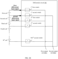
- the first switch group and the second switch group may be designed in the differential circuit 301.
- the first switch group may be configured to control a voltage signal flow direction of an odd-numbered cell
- the second switch group may be configured to control a voltage signal flow direction of an even-numbered cell.
- FIG. 2D is a schematic diagram of a differential circuit according to an embodiment of the present invention. It is assumed that N is an even number.
- one end of each first switch in the first switch group is connected to an odd-numbered cell in the N series-connected cells, and the other ends are jointly connected to the first output end 3011.
- One end of each second switch in the second switch group is connected to an even-numbered cell in the N series-connected cells, and the other ends are jointly connected to the second output end 3012.
- the first calibration switch 303 in FIG. 2A is in an on state; and when the i th first switch is in an on state and the i th second switch is in an off state, the differential circuit 301 is specifically configured to: receive a first differential input signal output by the (2i-1) th cell, and input, by using the i th first switch that is switched on, the first differential output signal to the first voltage division branch 3021 and the second voltage division branch 3022 that are connected in parallel; or when the i th first switch is in an off state and the i th second switch is in an on state, the differential circuit 301 is specifically configured to: receive a second differential input signal output by the 2i th cell, and input, by using the i th second switch that is switched on, the second differential output signal to the first voltage division branch 3021 and the second voltage division branch 3022 that are connected in parallel.
- the voltage sampling apparatus 30 is in a voltage signal calibration stage.
- the first voltage division branch 3021 and the second voltage division branch 3022 receive only one same voltage signal (the target signal mentioned above). Therefore, the i th first switch may be switched on, and the i th second switch may be switched off, to ensure that only a voltage signal of the (2i-1) th cell is input to the differential circuit 301, and the differential circuit 301 outputs only the first differential output signal.
- the i th second switch may be switched on, and the i th first switch may be switched off, to ensure that only a voltage signal of the 2i th cell is input to the differential circuit 301, and the differential circuit 301 outputs only the second differential output signal.
- a 1 st first switch may be switched on, and a 1 st second switch may be switched off, to input a voltage signal of the first cell to the differential circuit 301 to obtain the first differential output signal; or a 1 st second switch may be switched on, and a 1 st first switch is switched off, to input a voltage signal of a second cell to the differential circuit 301 to obtain the second differential output signal.
- the deviation signal is obtained based on the first differential output signal or the deviation signal is obtained based on the second differential output signal.
- the deviation signals can calibrate an error of a difference between the voltage division ratios provided by the two voltage division branches.
- the first calibration switch 303 in FIG. 2A is in an off state; and when both the i th first switch and the i th second switch are in an on state, the differential circuit 301 is specifically configured to: receive a first differential input signal output by the (2i-1) th cell and input the first differential output signal to the first voltage division branch 3021 by using the i th first switch that is switched on, and receive a second differential input signal output by the 2i th cell and input the second differential output signal to the second voltage division branch 3022 by using the i th second switch that is switched on.
- the voltage sampling apparatus 30 is in a voltage signal sampling stage.
- the first voltage division branch 3021 and the second voltage division branch 3022 receive two different voltage signals. Therefore, the i th first switch and the i th second switch may be switched on, to ensure that the differential circuit 301 can separately receive voltage signals of the (2i-1) th cell and the 2i th cell, and the differential circuit 301 can separately output two differential output signals (obtained based on the voltage signals of the (2i-1) th cell and the 2i th cell).
- FIG. 2E is a schematic diagram of a differential circuit in a voltage signal sampling stage according to an embodiment of the present invention.
- the 1 st first switch and the 1 st second switch are switched on, the voltage signal of the first cell is used as a first differential input signal, and the differential circuit 301 outputs a first differential output signal from the first output end 3011 based on the first differential input signal.
- the voltage signal of the second cell is used as a second differential input signal, and the differential circuit 301 outputs a second differential output signal from the second output end 3012 based on the second differential input signal.
- FIG. 2F is a schematic diagram of a back-to-back PMOS transistor according to an embodiment of the present invention. Because the back-to-back POMS transistor shown in the figure can prevent current backflow, the switches in the first switch group and the second switch group mentioned above may be specifically the back-to-back POMS transistor in the figure, to avoid current backflow to a cell.
- the apparatus is further optimized in the following descriptions, and is described in detail below.
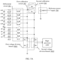
- FIG. 3A is a schematic diagram of another voltage sampling apparatus according to an embodiment of the present invention.
- the voltage sampling apparatus 30 in FIG. 2A may further include a second calibration switch 304.
- One end of the second calibration switch 304 is connected to the first end 3031 of the first calibration switch 303, and the other end is connected to a reference power supply 305.
- the voltage division circuit 302 is further configured to: receive, by using the second voltage division branch 3022, a reference voltage signal output by the reference power supply 305, and perform voltage division according to k 2 to output a fifth voltage signal, where the fifth voltage signal is used to calibrate k 2 . It should be noted that, according to the foregoing equation 2 and equation 3, it may be learned that, when an actual differential output signal (U difference1 -U difference2 ) is calculated, a coefficient before U difference1 -U difference2 affects a result.
- the second calibration switch 304 is added based on the voltage sampling apparatus 30 in FIG. 2A , and is externally connected to the reference power supply 305 and configured to calibrate a voltage division ratio of each voltage division branch in the voltage division circuit.
- the second voltage division branch 3022 in the voltage division circuit 302 can receive the voltage signal output by the reference power supply 305, and then the second voltage division branch 3022 performs voltage division on the voltage signal and outputs the fifth voltage signal.
- the reference power supply 305 can output a stable and known voltage signal.
- the voltage division ratio (k 2 ) of the second voltage division branch 3022 may be obtained based on a value of the fifth voltage signal that is output by the second voltage division branch 3022 after voltage division and a value of the voltage signal of the reference power supply 305, to calibrate the voltage division ratio of the second voltage division branch 3022.
- the calibration module is specifically configured to: when the target signal is the first differential output signal, restore, according to the calibrated kz, the second sampling signal as the sampling value of the difference between the first differential output signal and the second differential output signal. Specifically, the second sampling signal is restored, according to the calibrated second voltage division ratio, as the sampling value of the difference between the two voltage signals actually output by the differential circuit. This avoids a sampling error caused to sampling by the voltage division ratio, and further improves sampling precision of the voltage sampling apparatus.
- the voltage division circuit 302 in FIG. 3A is further configured to: receive, by using the first voltage division branch 3021, the reference voltage signal output by the reference power supply 305, and perform voltage division according to k 1 to output a sixth voltage signal, where the sixth voltage signal is used to calibrate k 1 .
- the first voltage division branch 3021 in the voltage division circuit 302 can receive the voltage signal output by the reference power supply 305, and then the first voltage division branch 3021 performs voltage division on the voltage signal and outputs the sixth voltage signal.
- the reference power supply 305 can output a stable and known voltage signal. Therefore, the voltage division ratio (ki) of the first voltage division branch 3021 may be obtained based on a value of the sixth voltage signal that is output by the first voltage division branch 3021 after voltage division and the value of the voltage signal of the reference power supply 305, to calibrate the voltage division ratio of the first voltage division branch 3021.
- the calibration module is specifically configured to: when the target signal is the second differential output signal, restore, according to the calibrated ki, the second sampling signal as the sampling value of the difference between the first differential output signal and the second differential output signal. Specifically, the second sampling signal is restored, according to the calibrated first voltage division ratio, as the sampling value of the difference between the two voltage signals actually output by the differential circuit. This avoids a sampling error caused to sampling by the voltage division ratio, and further improves sampling precision of the voltage sampling apparatus.
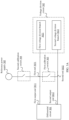
- FIG. 3B-1 and FIG. 3B-2 show a schematic diagram of a voltage sampling process based on another voltage sampling apparatus according to an embodiment of the present invention.
- the first calibration switch 303 and the second calibration switch 304 may be first switched on.
- the second voltage division branch 3022 receives the reference voltage signal output by the reference power supply 305, and performs voltage division to output the fifth voltage signal.
- the voltage division ratio k 2 of the second voltage division branch 3022 can be obtained through calculation based on the value of the fifth voltage signal and the value of the reference voltage signal.
- the first calibration switch 303 may be switched off.
- the first voltage division branch 3021 receives the reference voltage signal output by the reference power supply 305, and performs voltage division to output the sixth voltage signal.
- the voltage division ratio k 1 of the first voltage division branch 3011 can be obtained through calculation based on the value of the sixth voltage signal and the value of the reference voltage signal. Then, the second calibration switch 304 is switched off, and the first calibration switch 303 is switched on.
- the first voltage division branch 3021 and the second voltage division branch 3022 separately receive the target signal output by the differential circuit 301, and perform voltage division to separately output the first voltage signal and the second voltage signal and obtain the first deviation signal, that is, U difference1 (k 1 -k 2 ) or U difference2 (k 1 -k 2 ), based on the first voltage signal and the second voltage signal, to complete voltage signal calibration.
- the first calibration switch 303 is switched off.
- the first voltage division branch 3021 receives the first differential output signal, and performs voltage division to output the third voltage signal.
- the second voltage division branch 3022 receives the second differential output signal, and performs voltage division to output the fourth voltage signal.
- a differential sampling signal is obtained based on the third voltage signal and the fourth voltage signal, that is, U sampling -k 1 ⁇ U difference1 -k 2 ⁇ U difference2 . Further, the difference (U difference1 -U difference2 ) of the voltage signals actually output by the differential circuit 301 can be more accurately calculated according to the foregoing equation 2 or equation 3.
- a ground end of the first voltage division branch 3021 and a ground end of the second voltage division branch 3022 are both connected to a ground cable.
- the first voltage division branch 3021 includes M series-connected first voltage division resistors
- the second voltage division branch 3022 includes M series-connected second voltage division resistors
- M is an integer greater than 1.
- the voltage division circuit 302 is specifically configured to: perform, by using the M series-connected first voltage division resistors, voltage division on the target signal according to k 1 to output the first voltage signal, and perform, by using the M series-connected second voltage division resistors, voltage division on the target signal according to k 2 to output the second voltage signal.
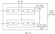
- the ground ends of the two voltage division branches in the voltage division circuit 302 are connected to the ground cable, and a voltage division element may be a plurality of series-connected resistors, to implement voltage division on an input voltage signal, to output a voltage signal that meets a voltage withstand limitation condition of the sampling chip. For example, as shown in FIG. 3C, FIG.
- 3C is a schematic diagram of a voltage division circuit according to an embodiment of the present invention.
- a voltage division element in the first voltage division branch 3021 is two series-connected resistors, that is, R1 and R2.
- a voltage division element in the second voltage division branch 3022 is two series-connected resistors, that is, R3 and R4.
- the voltage division circuit 302 when the first calibration switch 303 is in an off state, is specifically configured to: perform, by using the M series-connected first voltage division resistors, voltage division on the first differential output signal according to k 1 to output the third voltage signal, and perform, by using the M series-connected second voltage division resistors, voltage division on the second differential output signal according to k 2 to output the fourth voltage signal.
- the first voltage division branch 3021 receives the first differential output signal, and performs voltage division on the signal by using the voltage division resistors, to output the voltage signal obtained through voltage division.
- the second voltage division branch 3022 receives the second differential output signal, and performs voltage division on the signal by using the voltage division resistors, to output the voltage signal obtained through voltage division.
- FIG. 3D is a schematic diagram of still another voltage sampling apparatus according to an embodiment of the present invention.
- the voltage sampling apparatus 30 in FIG. 3A may further include an analog-to-digital converter 306.
- the analog-to-digital converter 306 is configured to: receive an output signal of the voltage division circuit 302, and convert the output signal from an analog signal into a digital signal, where the output signal includes the first voltage signal and the second voltage signal, or the third voltage signal and the fourth voltage signal, or the fifth voltage signal, or the sixth voltage signal.
- the analog-to-digital converter 306 is added based on the voltage sampling circuit in FIG. 3A , and is configured to convert an analog signal output by the voltage division circuit 302 into a digital signal, to facilitate subsequent digital operation.
- a differential sampling apparatus in a conventional technology is optimized to calibrate the voltage sampling signal. This improves sampling precision of the voltage sampling signal.
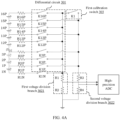
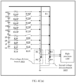
- FIG. 4A is a schematic diagram of a voltage sampling apparatus in which 16 cells are used as an example according to an embodiment of the present invention. It should be noted that in FIG. 4A , that the N series-connected cells connected to the differential circuit 301 in the voltage sampling apparatus 30 are 16 cells is used as an example, and each cell may be connected to the switch through a protective resistor.
- a voltage division element in the first voltage division branch 3021 is two series-connected resistors, that is, R1 and R2.
- a voltage division element in the second voltage division branch 3022 is two series-connected resistors, that is, R3 and R4.
- U 16P is the voltage signal of the first cell in FIG. 2D
- U 15P is the voltage signal of the second cell
- U 14P is a voltage signal of a third cell.
- U 1P is a voltage signal of a sixteenth cell.
- K16P is the 1 st first switch in FIG. 2D
- K15P is the 1 st second switch
- K14P is a 2 nd first switch.
- K1P is an 8 th second switch.
- K1 is the first calibration switch 303 in FIG. 2A .
- FIG. 4B is a flowchart of a sampling process in which 16 cells are used as an example according to an embodiment of the present invention.
- the sixteenth cell (the first cell in FIG. 2D ) is first sampled, and K16P and K1 are switched on, to obtain a first deviation signal, that is, U 16P (k 1 -k 2 ).
- FIG. 4C(a) to FIG. 4C(d) show a detailed schematic flowchart of sampling voltage signals of 16 cells according to an embodiment of the present invention.
- sampling is performed on a fifteenth cell (the second cell in FIG. 2D ), K16P and K15P are switched off, and then K15P and K1 are switched on, to obtain a first deviation signal, that is, U 15P (k 1 -k 2 ).
- U 15P enters the first voltage division branch 3021 and the second voltage division branch 3022 for voltage division, to obtain U 15P (k 1 -k 2 ).
- K1 is switched off, and K15P and K14P are switched on, to obtain a differential sampling signal U sampling15 .
- FIG. 4C(c) when K15P and K1 are switched on, U 15P enters the first voltage division branch 3021 and the second voltage division branch 3022 for voltage division, to obtain U 15P (k 1 -k 2 ).
- K1 is switched off, and K15P and K14P are switched on, to obtain a differential sampling signal U sampling15 .
- FIG. 4C(c) when K15P and K1 are switched on, U 15P enters the
- FIG. 4D is a flowchart of another sampling process in which 16 cells are used as an example according to an embodiment of the present invention.
- K16P and K15P are switched off, and then K15P and K14P are switched on, to obtain a differential sampling signal U sampling15 .
- a more actual differential output signal (U 15P -U 14P ) of the fifteenth cell can be reversely calculated according to the equation 5.
- voltage signals of the 16 cells can be collected in sequence. Details are not described herein again.
- calibration needs to be performed once before sampling is performed on each cell.
- calibration may be performed once before sampling is performed on every two cells. In other words, an odd-numbered cell and an even-numbered cell share a calibration result. This can improve a sampling speed.
- FIG. 5A is a schematic diagram of another voltage sampling apparatus in which 16 cells are used as an example according to an embodiment of the present invention. It should be noted that in FIG. 5A , that the N series-connected cells connected to the differential circuit 301 in the voltage sampling apparatus 30 are 16 cells is used as an example.
- a voltage division element in the first voltage division branch 3021 is two series-connected resistors, that is, R1 and R2.
- a voltage division element in the second voltage division branch 3022 is two series-connected resistors, that is, R3 and R4.
- U 16P is the voltage signal of the first cell in FIG.
- U 15P is the voltage signal of the second cell
- U 14P is a voltage signal of a third cell.
- U 1P is a voltage signal of a sixteenth cell.
- K16P is the 1 st first switch in FIG. 2D
- K15P is the 1 st second switch
- K14P is a 2 nd first switch.
- K1P is an 8 th second switch.
- K1 is the first calibration switch 303 in FIG. 3A .
- K2 is the second calibration switch 304 in FIG. 3A .
- FIG. 5B is a flowchart of still another sampling process in which 16 cells are used as an example according to an embodiment of the present invention.
- K1 and K2 may be first switched on, to obtain a calibrated voltage division ratio k 2 of the second voltage division branch.
- FIG. 5C(a) and FIG. 5C(b) show another detailed schematic flowchart of sampling voltage signals of 16 cells according to an embodiment of the present invention.
- FIG. 5C(a) K1 and K2 in FIG.
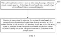
- FIG. 6 is a flowchart of a voltage sampling method according to an embodiment of the present invention.
- the method is applicable to any voltage sampling apparatus in FIG. 2A , FIG. 3A , and FIG. 3D and a device including the voltage sampling apparatus.
- the method may include the following steps S601 and S602.
- the voltage sampling apparatus includes a differential circuit, a voltage division circuit, and a first calibration switch.
- the voltage division circuit includes a first voltage division branch and a second voltage division branch. A first output end of the differential circuit and an input end of the first voltage division branch are connected to a first end of the first calibration switch. A second output end of the differential circuit and an input end of the second voltage division branch are connected to a second end of the first calibration switch.
- Step S601 When the first calibration switch is in an on state, input, by using the differential circuit, a target signal to the first voltage division branch and the second voltage division branch that are connected in parallel.
- the target signal is a first differential output signal output by the first output end or a second differential output signal output by the second output end.
- Step S602 Receive the target signal by using the first voltage division branch of the voltage division circuit and perform voltage division according to a first voltage division ratio k 1 to output a first voltage signal, and receive the target signal by using the second voltage division branch and perform voltage division according to a second voltage division ratio k 2 to output a second voltage signal.
- a difference between the first voltage signal and the second voltage signal is a first deviation signal
- the first deviation signal is used to calibrate a difference between the first voltage division ratio and the second voltage division ratio.
- the first voltage division branch and the second voltage division branch are switched from a parallel-connected state to an open-circuit state.
- the method further includes: inputting the first differential output signal to the first voltage division branch through the first output end of the differential circuit, and inputting the second differential output signal to the second voltage division branch through the second output end; and receiving the first differential output signal by using the first voltage division branch of the voltage division circuit and performing voltage division according to k 1 to output a third voltage signal, and receiving the second differential output signal by using the second voltage division branch and performing voltage division according to k 2 to output a fourth voltage signal, where a difference between the third voltage signal and the fourth voltage signal is a first sampling signal.
- the voltage sampling apparatus further includes a calibration module.
- the method further includes: obtaining, by using the calibration module, a second sampling signal through calculation based on the first deviation signal and the first sampling signal, where the second sampling signal indicates a difference between voltage signals obtained after voltage division is performed on the first differential output signal and the second differential output signal according to a same voltage division ratio, and the same voltage division ratio is the first voltage division ratio or the second voltage division ratio; and when the target signal is the first differential output signal, restoring, by using the calibration module according to kz, the second sampling signal as a sampling value of a difference between the first differential output signal and the second differential output signal; or when the target signal is the second differential output signal, restoring, by using the calibration module according to ki, the second sampling signal as a sampling value of a difference between the first differential output signal and the second differential output signal.
- the first calibration switch is in an on state.
- the inputting, by using the differential circuit, a target signal to the first voltage division branch and the second voltage division branch that are connected in parallel includes: when the i th first switch is in an on state and the i th second switch is in an off state, receiving, by using the differential circuit, a first differential input signal output by the (2i-1) th cell, and inputting, by using the i th first switch that is switched on, the first differential output signal to the first voltage division branch and the second voltage division branch that are connected in parallel; or when the i th first switch is in an off state and the i th second switch is in an on state, receiving, by using the differential circuit, a second differential input signal output by the 2i th cell, and inputting, by using the i th second switch that is switched on, the second differential output signal to the first voltage division branch and the second voltage division branch that are connected in parallel.
- the first calibration switch is in an off state.
- the inputting the first differential output signal to the first voltage division branch through the first output end of the differential circuit, and inputting the second differential output signal to the second voltage division branch through the second output end includes: when both the i th first switch and the i th second switch are in an on state, receiving, by using the differential circuit, a first differential input signal output by the (2i-1) th cell and inputting the first differential output signal to the first voltage division branch by using the i th first switch that is switched on, and receiving a second differential input signal output by the 2i th cell and inputting the second differential output signal to the second voltage division branch by using the i th second switch that is switched on.
- the voltage sampling apparatus further includes a second calibration switch.
- One end of the second calibration switch is connected to the first end of the first calibration switch, and the other end is connected to a reference power supply.
- the method further includes: receiving, by using the second voltage division branch of the voltage division circuit, a reference voltage signal output by the reference power supply, and performing voltage division according to k 2 to output a fifth voltage signal, where the fifth voltage signal is used to calibrate k 2 .
- the restoring, according to kz, the second sampling signal as a sampling value of a difference between the first differential output signal and the second differential output signal when the target signal is the first differential output signal includes: when the target signal is the first differential output signal, restoring, by using the calibration module according to the calibrated kz, the second sampling signal as the sampling value of the difference between the first differential output signal and the second differential output signal.
- the method further includes: receiving, by using the first voltage division branch of the voltage division circuit, the reference voltage signal output by the reference power supply, and performing voltage division according to k 1 to output a sixth voltage signal, where the sixth voltage signal is used to calibrate k 1 .
- the restoring, according to ki, the second sampling signal as a sampling value of a difference between the first differential output signal and the second differential output signal when the target signal is the second differential output signal includes: when the target signal is the second differential output signal, restoring, by using the calibration module according to the calibrated ki, the second sampling signal as the sampling value of the difference between the first differential output signal and the second differential output signal.
- a ground end of the first voltage division branch and a ground end of the second voltage division branch are both connected to a ground cable.
- the first voltage division branch includes M series-connected first voltage division resistors
- the second voltage division branch includes M series-connected second voltage division resistors
- M is an integer greater than 1.
- the receiving the target signal by using the first voltage division branch of the voltage division circuit and performing voltage division to output a first voltage signal, and receiving the target signal by using the second voltage division branch and performing voltage division to output a second voltage signal includes: performing, by using the M series-connected first voltage division resistors of the voltage division circuit, voltage division on the target signal according to k 1 to output the first voltage signal, and performing, by using the M series-connected second voltage division resistors, voltage division on the target signal according to k 2 to output the second voltage signal.
- the receiving the first differential output signal by using the first voltage division branch of the voltage division circuit and performing voltage division to output a third voltage signal, and receiving the second differential output signal by using the second voltage division branch and performing voltage division to output a fourth voltage signal includes: performing, by using the M series-connected first voltage division resistors of the voltage division circuit, voltage division on the first differential output signal according to k 1 to output the third voltage signal, and performing, by using the M series-connected second voltage division resistors, voltage division on the second differential output signal according to k 2 to output the fourth voltage signal.
- the voltage sampling apparatus further includes an analog-to-digital converter.
- the method further includes: receiving, by using the analog-to-digital converter, an output signal of the voltage division circuit, and converting the output signal from an analog signal into a digital signal, where the output signal includes the first voltage signal and the second voltage signal, or the third voltage signal and the fourth voltage signal, or the fifth voltage signal, or the sixth voltage signal.
- the terminal device has a function of implementing the method according to any one of the foregoing voltage sampling method embodiments.
- the function may be implemented by hardware, or may be implemented by hardware executing corresponding software.
- the hardware or the software includes one or more modules corresponding to the function.
- the terminal device includes a processor.
- the processor is configured to support the terminal device in performing a corresponding function in the voltage sampling method provided above.
- the terminal device may further include a memory.
- the memory is coupled to the processor, and stores program instructions and data that are necessary for the terminal device.
- the terminal device may further include a communication interface, configured to implement communication between the terminal device and another device or a communication network.
- An embodiment of the present invention provides a computer program.
- the computer program includes instructions.
- the computer program is executed by a computer, the computer is enabled to perform a procedure in the voltage sampling method according to any one of the foregoing embodiments.
- the chip system includes a processor, configured to support an application server or a terminal device in implementing a function in the foregoing voltage sampling apparatus, for example, generating or processing information in the foregoing method.
- the chip system further includes a memory.
- the memory is configured to store program instructions and data that are necessary for a data sending device.
- the chip system may include a chip, or may include a chip and another discrete component.
- the semiconductor chip includes the voltage sampling apparatus according to any one of the foregoing embodiments.
- the electronic device includes the foregoing semiconductor chip.
- the disclosed apparatus may be implemented in other manners.
- the described apparatus embodiment is merely an example.
- division into the units is merely logical function division and may be other division in actual implementation.
- a plurality of units or components may be combined or integrated into another system, or some features may be ignored or not performed.
- the displayed or discussed mutual connections or direct connections or communication connections may be implemented by using some interfaces.
- the indirect connections or communication connections between the apparatuses or units may be implemented in electronic or other forms.
- different modules in the apparatus may be indirectly connected by using a protection element, or may be directly connected between different modules.
- the foregoing units described as separate parts may or may not be physically separate, and parts displayed as units may or may not be physical units, may be located in one position, or may be distributed on a plurality of network units. Some or all of the units may be selected based on actual requirements to achieve the objectives of the solutions of embodiments.
- functional units in embodiments of this application may be integrated into one processing unit, or each of the units may exist alone physically, or two or more units are integrated into one unit.
- the integrated unit may be implemented in a form of hardware, or may be implemented in a form of a software functional unit.
- the integrated unit When the foregoing integrated unit is implemented in the form of a software functional unit and sold or used as an independent product, the integrated unit may be stored in a computer-readable storage medium. Based on such an understanding, the technical solutions of this application essentially, or the part contributing to the prior art, or all or some of the technical solutions may be implemented in the form of a software product.
- the software product is stored in a storage medium and includes several instructions for instructing a computer device (which may be a personal computer, a server, or a network device) to perform all or some of the steps of the methods described in embodiments of this application.
- the foregoing storage medium includes any medium that can store program code, such as a USB flash drive, a removable hard disk, a magnetic disk, an optical disc, a read-only memory (Read-Only Memory, ROM for short), or a random access memory (Random Access Memory, RAM for short).
- program code such as a USB flash drive, a removable hard disk, a magnetic disk, an optical disc, a read-only memory (Read-Only Memory, ROM for short), or a random access memory (Random Access Memory, RAM for short).
Landscapes
- Physics & Mathematics (AREA)
- General Physics & Mathematics (AREA)
- Measurement Of Current Or Voltage (AREA)
Applications Claiming Priority (1)
| Application Number | Priority Date | Filing Date | Title |
|---|---|---|---|
| PCT/CN2021/107869 WO2023000258A1 (fr) | 2021-07-22 | 2021-07-22 | Appareil d'échantillonnage de tension et procédé associé |
Publications (2)
| Publication Number | Publication Date |
|---|---|
| EP4354155A1 true EP4354155A1 (fr) | 2024-04-17 |
| EP4354155A4 EP4354155A4 (fr) | 2024-08-07 |
Family
ID=84980343
Family Applications (1)
| Application Number | Title | Priority Date | Filing Date |
|---|---|---|---|
| EP21950511.2A Pending EP4354155A4 (fr) | 2021-07-22 | 2021-07-22 | Appareil d'échantillonnage de tension et procédé associé |
Country Status (4)
| Country | Link |
|---|---|
| US (1) | US12638476B2 (fr) |
| EP (1) | EP4354155A4 (fr) |
| CN (1) | CN117413186A (fr) |
| WO (1) | WO2023000258A1 (fr) |
Families Citing this family (2)
| Publication number | Priority date | Publication date | Assignee | Title |
|---|---|---|---|---|
| CN118962547B (zh) * | 2024-07-22 | 2026-03-03 | 湖北魔方新能源科技有限公司 | 一种燃料电池电压采集精度软件补偿校准方法 |
| CN121231841B (zh) * | 2025-12-02 | 2026-03-06 | 恩智技术股份有限公司 | 电压采样方法、源载一体机、装置、设备及介质 |
Family Cites Families (16)
| Publication number | Priority date | Publication date | Assignee | Title |
|---|---|---|---|---|
| US5831427A (en) * | 1996-12-11 | 1998-11-03 | Elsyn, Inc. | Voltage measuring device for a source with unknown resistance |
| DE102005002570A1 (de) * | 2005-01-19 | 2006-07-27 | Infineon Technologies Ag | Ansteuerschaltung für zwei Schaltwandlerstufen eines Spannungswandlers |
| JP4561921B2 (ja) * | 2008-04-04 | 2010-10-13 | 株式会社デンソー | 電圧検出装置、及び電池の状態制御装置 |
| JP2011038876A (ja) * | 2009-08-10 | 2011-02-24 | Yazaki Corp | 複数組電池の電圧測定装置 |
| CN101915897A (zh) * | 2010-07-20 | 2010-12-15 | 安徽鑫龙电器股份有限公司 | 一种电池巡检仪及电池电压采集方法 |
| CN201774453U (zh) * | 2010-08-26 | 2011-03-23 | Bcd半导体制造有限公司 | 一种开关电源的电源电压检测电路 |
| JP6432201B2 (ja) * | 2014-03-17 | 2018-12-05 | 富士電機株式会社 | 半導体装置および半導体装置の製造方法 |
| CN103884900B (zh) * | 2014-03-31 | 2016-09-07 | 河南理工大学 | 一种变频调速器的直流母线电压检测装置及方法 |
| CN105629029B (zh) * | 2014-11-27 | 2018-07-06 | 华润矽威科技(上海)有限公司 | 电池包电压检测系统及检测方法 |
| CN106950407A (zh) * | 2017-02-14 | 2017-07-14 | 武汉合康动力技术有限公司 | 一种三相隔离检测电路 |
| CN108663622B (zh) * | 2017-03-30 | 2020-06-12 | 深圳市理邦精密仪器股份有限公司 | 电池组电压测量电路及电压测量系统 |
| GB201801910D0 (en) * | 2018-02-06 | 2018-03-21 | Analog Devices Global Unlimited Co | A non-contacting voltage measuring apparatus |
| JP2021005951A (ja) * | 2019-06-26 | 2021-01-14 | 日本電産サーボ株式会社 | 制御回路、及び校正システム |
| CN110174635B (zh) * | 2019-06-28 | 2021-08-31 | 蜂巢能源科技有限公司 | 高压采样板校准系统及方法 |
| JP2021043118A (ja) * | 2019-09-12 | 2021-03-18 | 株式会社豊田自動織機 | 電圧計測回路 |
| CN117716519A (zh) * | 2021-08-03 | 2024-03-15 | 索尼半导体解决方案公司 | 负电压监测电路和光接收装置 |
-
2021
- 2021-07-22 EP EP21950511.2A patent/EP4354155A4/fr active Pending
- 2021-07-22 CN CN202180098948.3A patent/CN117413186A/zh active Pending
- 2021-07-22 WO PCT/CN2021/107869 patent/WO2023000258A1/fr not_active Ceased
-
2024
- 2024-01-22 US US18/419,284 patent/US12638476B2/en active Active
Also Published As
| Publication number | Publication date |
|---|---|
| EP4354155A4 (fr) | 2024-08-07 |
| WO2023000258A1 (fr) | 2023-01-26 |
| US20240159798A1 (en) | 2024-05-16 |
| CN117413186A (zh) | 2024-01-16 |
| US12638476B2 (en) | 2026-05-26 |
Similar Documents
| Publication | Publication Date | Title |
|---|---|---|
| US20240159798A1 (en) | Voltage sampling apparatus and related method | |
| Dubarry et al. | Cell-balancing currents in parallel strings of a battery system | |
| CN101529646B (zh) | 用于监控和平衡电池组中的电池的方法和系统 | |
| Lee et al. | Development of a hardware-in-the-loop simulation system for testing cell balancing circuits | |
| CN110426645B (zh) | 多通道充放电参数校准方法及系统 | |
| EP3629439A1 (fr) | Procédé de commande de production d'énergie photovoltaïque, et système de production d'énergie photovoltaïque | |
| CN108663622B (zh) | 电池组电压测量电路及电压测量系统 | |
| CN109709489A (zh) | 一种计算电池功率限值的方法及系统 | |
| CN107305224A (zh) | 光伏逆变器的绝缘阻抗检测电路、检测方法及光伏逆变器 | |
| CN101303396A (zh) | 燃料电池性能监测系统 | |
| CN107450031A (zh) | 一种动力电池系统ocv‑soc函数关系的重构方法 | |
| US20110273182A1 (en) | Detecting the voltage in battery cells | |
| AU2023328496A1 (en) | Battery system and battery pack connection state identification method | |
| KR20160072410A (ko) | 배터리의 전압을 측정하기 위한 장치 및 그 방법 | |
| JP4616875B2 (ja) | 電圧検出装置 | |
| EP2693228A1 (fr) | Dispositif de surveillance de tension de cellule et d'étalonnage automatique | |
| US9465082B2 (en) | Device and method for measuring a maximum cell voltage | |
| US20210376616A1 (en) | System and method for balancing state of charge of battery | |
| EP3879619A1 (fr) | Procédé et système pour l'étalonnage d'un capteur de courant | |
| JP5615879B2 (ja) | 電池電圧監視装置及び自己校正装置 | |
| EP4207548B1 (fr) | Appareil de gestion de batterie et son procédé de fonctionnement | |
| KR101268847B1 (ko) | 배터리의 셀 전압 측정장치 및 그 측정방법 | |
| JP2024139761A (ja) | バッテリsoc補正方法、バッテリsoc補正装置、及びその方法を実行させるために記録媒体に保存されているコンピュータプログラム | |
| US12519402B2 (en) | Controllers for chain-link converters | |
| Fedchenko et al. | Static accuracy of the automated stand for lithiumion batteries testing |
Legal Events
| Date | Code | Title | Description |
|---|---|---|---|
| STAA | Information on the status of an ep patent application or granted ep patent |
Free format text: STATUS: THE INTERNATIONAL PUBLICATION HAS BEEN MADE |
|
| PUAI | Public reference made under article 153(3) epc to a published international application that has entered the european phase |
Free format text: ORIGINAL CODE: 0009012 |
|
| STAA | Information on the status of an ep patent application or granted ep patent |
Free format text: STATUS: REQUEST FOR EXAMINATION WAS MADE |
|
| 17P | Request for examination filed |
Effective date: 20240109 |
|
| AK | Designated contracting states |
Kind code of ref document: A1 Designated state(s): AL AT BE BG CH CY CZ DE DK EE ES FI FR GB GR HR HU IE IS IT LI LT LU LV MC MK MT NL NO PL PT RO RS SE SI SK SM TR |
|
| A4 | Supplementary search report drawn up and despatched |
Effective date: 20240709 |
|
| RIC1 | Information provided on ipc code assigned before grant |
Ipc: G01R 19/00 20060101AFI20240703BHEP |
|
| DAV | Request for validation of the european patent (deleted) | ||
| DAX | Request for extension of the european patent (deleted) |