EP4354664A1 - Structure de connexion supraconductrice de tige de fil supraconducteur en nb3sn et tige de fil en nbti, son procédé de production et appareil à résonance magnétique nucléaire l'utilisant - Google Patents
Structure de connexion supraconductrice de tige de fil supraconducteur en nb3sn et tige de fil en nbti, son procédé de production et appareil à résonance magnétique nucléaire l'utilisant Download PDFInfo
- Publication number
- EP4354664A1 EP4354664A1 EP22819987.3A EP22819987A EP4354664A1 EP 4354664 A1 EP4354664 A1 EP 4354664A1 EP 22819987 A EP22819987 A EP 22819987A EP 4354664 A1 EP4354664 A1 EP 4354664A1
- Authority
- EP
- European Patent Office
- Prior art keywords
- superconducting
- cores
- nbti
- wire
- alloy strips
- Prior art date
- Legal status (The legal status is an assumption and is not a legal conclusion. Google has not performed a legal analysis and makes no representation as to the accuracy of the status listed.)
- Granted
Links
Images






Classifications
-
- H—ELECTRICITY
- H02—GENERATION; CONVERSION OR DISTRIBUTION OF ELECTRIC POWER
- H02G—INSTALLATION OF ELECTRIC CABLES OR LINES, OR OF COMBINED OPTICAL AND ELECTRIC CABLES OR LINES
- H02G1/00—Methods or apparatus specially adapted for installing, maintaining, repairing or dismantling electric cables or lines
- H02G1/14—Methods or apparatus specially adapted for installing, maintaining, repairing or dismantling electric cables or lines for joining or terminating cables
-
- H—ELECTRICITY
- H01—ELECTRIC ELEMENTS
- H01B—CABLES; CONDUCTORS; INSULATORS; SELECTION OF MATERIALS FOR THEIR CONDUCTIVE, INSULATING OR DIELECTRIC PROPERTIES
- H01B12/00—Superconductive or hyperconductive conductors, cables, or transmission lines
- H01B12/02—Superconductive or hyperconductive conductors, cables, or transmission lines characterised by their form
-
- H—ELECTRICITY
- H01—ELECTRIC ELEMENTS
- H01F—MAGNETS; INDUCTANCES; TRANSFORMERS; SELECTION OF MATERIALS FOR THEIR MAGNETIC PROPERTIES
- H01F6/00—Superconducting magnets; Superconducting coils
- H01F6/06—Coils, e.g. winding, insulating, terminating or casing arrangements therefor
- H01F6/065—Feed-through bushings, terminals and joints
-
- H—ELECTRICITY
- H10—SEMICONDUCTOR DEVICES; ELECTRIC SOLID-STATE DEVICES NOT OTHERWISE PROVIDED FOR
- H10N—ELECTRIC SOLID-STATE DEVICES NOT OTHERWISE PROVIDED FOR
- H10N60/00—Superconducting devices
- H10N60/80—Constructional details
-
- H—ELECTRICITY
- H01—ELECTRIC ELEMENTS
- H01R—ELECTRICALLY-CONDUCTIVE CONNECTIONS; STRUCTURAL ASSOCIATIONS OF A PLURALITY OF MUTUALLY-INSULATED ELECTRICAL CONNECTING ELEMENTS; COUPLING DEVICES; CURRENT COLLECTORS
- H01R4/00—Electrically-conductive connections between two or more conductive members in direct contact, i.e. touching one another; Means for effecting or maintaining such contact; Electrically-conductive connections having two or more spaced connecting locations for conductors and using contact members penetrating insulation
- H01R4/58—Electrically-conductive connections between two or more conductive members in direct contact, i.e. touching one another; Means for effecting or maintaining such contact; Electrically-conductive connections having two or more spaced connecting locations for conductors and using contact members penetrating insulation characterised by the form or material of the contacting members
- H01R4/68—Connections to or between superconductive connectors
-
- H—ELECTRICITY
- H02—GENERATION; CONVERSION OR DISTRIBUTION OF ELECTRIC POWER
- H02G—INSTALLATION OF ELECTRIC CABLES OR LINES, OR OF COMBINED OPTICAL AND ELECTRIC CABLES OR LINES
- H02G15/00—Cable fittings
- H02G15/34—Cable fittings for cryogenic cables
-
- H—ELECTRICITY
- H10—SEMICONDUCTOR DEVICES; ELECTRIC SOLID-STATE DEVICES NOT OTHERWISE PROVIDED FOR
- H10N—ELECTRIC SOLID-STATE DEVICES NOT OTHERWISE PROVIDED FOR
- H10N60/00—Superconducting devices
- H10N60/01—Manufacture or treatment
- H10N60/0156—Manufacture or treatment of devices comprising Nb or an alloy of Nb with one or more of the elements of group IVB, e.g. titanium, zirconium or hafnium
-
- H—ELECTRICITY
- H10—SEMICONDUCTOR DEVICES; ELECTRIC SOLID-STATE DEVICES NOT OTHERWISE PROVIDED FOR
- H10N—ELECTRIC SOLID-STATE DEVICES NOT OTHERWISE PROVIDED FOR
- H10N60/00—Superconducting devices
- H10N60/01—Manufacture or treatment
- H10N60/0184—Manufacture or treatment of devices comprising intermetallic compounds of type A-15, e.g. Nb3Sn
Definitions
- the present invention relates to a superconducting joint structural body in which a Nb 3 Sn superconducting wire and a NbTi wire are jointed, a method for manufacturing the same, and an NMR analyzer that uses the same.
- a magnet for orienting nuclear spin in a nuclear magnetic resonance (NMR) apparatus is driven in a persistent current mode for a precise NMR measurement.
- NMR nuclear magnetic resonance
- a technique of realizing a joint between superconducting wires having a limited length at zero resistance which is so-called superconducting joint technique, has been desired.
- superconducting joint is essential not only between NbTi superconducting wires, but also between different superconducting materials of a NbTi superconducting wire and a Nb 3 Sn superconducting wire used for high magnetic field application.
- NbTi As for NbTi, it has known that the NbTi is an alloy prepared by solid-solving Ti into a body-centered cubic lattice of Nb, and thus has ductility and toughness, and that the superconducting joint thereof can be achieved also by means of mechanical pressure welding (see “Patent Literature 1", for example).
- Nb 3 Sn is an A15-type compound crystal composed of Nb atoms and Sn atoms in a ratio of 3:1, has no ductility, and is hard and brittle. Therefore, the joint by means of a mechanical method has been impossible.
- Patent Literature 2 As a substitute means for the joint by means of a mechanical method, a superconducting joint technique of utilizing a low-melting-point superconducting solder has been developed (see “Patent Literature 2" and “Non-Patent Literature 1", for example).
- Patent Literature 2 the following method is disclosed. At the ends of NbTi and Nb 3 Sn multi-core wires, a Cu matrix embedding superconducting filaments is melted in molten Sn or molten Sn alloy, thereby directly coating the filaments with Sn. Next, the ends of both the wires are immersed in molten Pb-Bi to replace Sn with Pb-Bi.
- the ends of both the wires are immersed in a cup filled with Pb-Bi to form a joint portion, thereby realizing a superconducting joint between the NbTi wire and Nb 3 Sn wire.
- the NbTi and the Nb 3 Sn filaments that are easily oxidized can be in close contact with the superconductive Pb-Bi without exposing their surfaces to the air as well as without applying thereto mechanical deformation, thereby realizing a good superconducting joint between the NbTi wire and Nb 3 Sn wire through the Pb-Bi superconducting joint.
- This joint has the superconducting properties that depend on the properties of Pb-Bi, and is ordinarily used in a magnetic environment of 0.5 to 1.0 T.
- Non-Patent Literature 1 a superconducting joint technique of using other low-melting-point superconducting solders such as Wood's metal (50%Bi-24%Pb-14%Sn-12%Cd), Pb-In, and Sn-In is disclosed. Many of them that are highly practical as well as that have relatively high critical magnetic field contain Pb and Cd of environmentally hazardous substances.
- Non-Patent Literature 2 a recent study on Nb 3 Sn tissue control has reported that Hf increases recovery and recrystallization temperatures of Nb (see “Non-Patent Literature 2", for example).
- FIG. 1 of “Non-Patent Literature 2” it is reported that Nb-4at%Ta-1at%Hf alloy prepared by adding 1 at% of Hf and 4 at% of Ta to Nb maintains densification thereof even after performing an annealing treatment at 900°C.
- FIG. 2 of “Non-Patent Literature 2” it is reported that as a result of a study on the recovery and recrystallization temperatures of a Nb-Hf alloy prepared by adding only Hf to Nb, the recovery temperature was found to greatly exceed 600°C.
- the conventional superconducting joint technique for jointing the Nb 3 Sn superconducting wire and the NbTi wire uses environmentally hazardous substances such as Pb and Cd.
- Non-Patent Literature 2 relates to only the tissue control study of Nb 3 Sn itself, and gives neither teaching nor suggestion on a superconducting joint between different superconducting materials (e.g., a superconducting joint between the Nb 3 Sn superconducting wire and the NbTi wire).
- the superconducting joint structural body of the present invention comprises: a joint strip having one or more of Nb alloy strips to which an element M is added (wherein the element M is an element that increases a recovery temperature and a recrystallization temperature of Nb); a Nb 3 Sn superconducting wire having one or more of Nb 3 Sn superconducting cores; and a NbTi wire having one or more of NbTi cores, wherein one end of the joint strip is jointed with the Nb 3 Sn superconducting wire by contact with each of the one or more of Nb alloy strips and each of the one or more of Nb 3 Sn superconducting cores through a Nb 3 Sn superconducting layer, and the other end of the joint strip is jointed with the NbTi wire by mutual contact with each bare surface of the one or more of Nb alloy strips and each bare surface of the one or more of NbTi cores, thereby solving the above problems.
- the above element M may be at least one selected from the group consisting of hafnium (Hf), titanium (Ti), tantalum (Ta), zirconium (Zr), and tungsten (W).
- the above Nb alloy strip may have any one shape selected from the group consisting of a core, a sheet, and a pipe.
- the above strip in the present application means a band-like long and thin one formed in the shape of a core, a sheet, a pipe or the like.
- the above element M may be added in a range from 0.2 at% or more to 10 at% or less (wherein the unit "at%" means atomic percentage of the above element M contained in the one or more of Nb alloy strips).
- Each of a portion where each of the one or more of Nb alloy strips and each of the one or more of Nb 3 Sn superconducting cores are in contact with each other through a Nb 3 Sn superconducting layer and a portion where each bare surface of the one or more of Nb alloy strips and each bare surface of the one or more of NbTi cores are in mutual contact may be covered by means of a crimp tube made of at least one material selected from the group consisting of tantalum (Ta), niobium (Nb), copper-nickel alloy (CuNi), and stainless steel.
- Each of the above covered portions may have a length in a range from 10 mm or more to 30 mm or less.
- the above joint strip may have the following structures: each of the one or more of Nb alloy strips is covered with and/or embedded in a first stabilizer; the Nb 3 Sn superconducting wire has the one or more of Nb 3 Sn superconducting cores each of which is covered with and/or embedded in a second stabilizer; the NbTi wire has the one or more of NbTi cores each of which is covered with and/or embedded in a third stabilizer; and each of the first to third stabilizers is at least one metal selected from the group consisting of copper metal, copper alloy, silver metal, and silver alloy.
- a method for manufacturing the above superconducting joint structural body of the present invention comprises the steps of: a first jointing step for jointing one end of a joint strip having one or more of Nb alloy strips to which an element M is added (wherein the element M is an element that increases a recovery temperature and a recrystallization temperature of Nb) and a Nb 3 Sn superconducting wire having one or more of Nb 3 Sn superconducting cores; and a second jointing step for jointing the other end of the joint strip and a NbTi wire having one or more of NbTi cores, the first jointing step comprising the steps of: a step of exposing the one or more of Nb alloy strips from one end of the joint strip; a step of exposing the one or more of Nb cores from one end of a Nb 3 Sn superconducting precursor wire having one or more of Nb cores that are embedded in a matrix that contains at least Cu and Sn; a step of bundling the exposed one or more of Nb
- the above step of exposing the one or more of Nb alloy strips in the first jointing step and the above step of exposing the one or more of Nb alloy strips in the second jointing step may be performed by means of chemical corrosion.
- the above step of exposing the one or more of Nb cores in the first jointing step may be performed by means of chemical corrosion.
- the above step of exposing the one or more of Nb cores in the first jointing step may be further performed by means of mechanical polishing.
- the above step of exposing the one or more of NbTi cores in the second jointing step may be performed by means of chemical corrosion.
- each of the following steps: the step of exposing the one or more of Nb alloy strips in the first jointing step and the step of exposing the one or more of Nb alloy strips in the second jointing step; the step of exposing the one or more of Nb cores in the first jointing step; and the step of exposing the one or more of NbTi cores in the second jointing step may be performed so that any exposed length is in a range from 10 mm or more and 30 mm or less.
- the above crimping step in the first jointing step may be performed by exposing each bare surface of the one or more of Nb alloy strips and each bare surface of the one or more of Nb cores, and by being the each bare surface of the one or more of Nb alloy strips and the each bare surface of the one or more of Nb cores in close contact with each other.
- the above crimping step in the first jointing step may be performed by covering a portion bundling the one or more of Nb alloy strips and the one or more of Nb cores by means of a crimp tube made of at least one material selected from the group consisting of tantalum (Ta), niobium (Nb), copper-nickel alloy (CuNi), and stainless steel, and applying a pressure in a perpendicular direction to a longitudinal direction of the one or more of Nb alloy strips and the one or more of Nb cores that are bundled together.
- a crimp tube made of at least one material selected from the group consisting of tantalum (Ta), niobium (Nb), copper-nickel alloy (CuNi), and stainless steel
- the above pressure may be in a range from 100 MPa or more to 1 GPa or less.
- the above annealing step in the first jointing step may be performed by means of an annealing treatment of the joint strip and the Nb 3 Sn superconducting precursor wire, in vacuum or in an inert gas atmosphere, within a temperature range from 600°C or more to 800°C or less.
- the above annealing step in the first jointing step may be performed by means of an annealing treatment of the joint strip and the Nb 3 Sn superconducting precursor wire, in vacuum or in an inert gas atmosphere, within a temperature range from 300°C or more to 500°C or less for 50 hours or more to 150 hours or less, and then within a temperature range from 600°C or more to 800°C or less for 50 hours or more to 150 hours or less.
- the above crimping step in the second jointing step may be performed by exposing each bare surface of the one or more of Nb alloy strips and the one or more of NbTi cores, and by being the each bare surface of the one or more of Nb alloy strips and the each bare surface of the one or more of NbTi cores in close contact with each other.
- the above crimping step in the second jointing step may be performed by covering a portion bundling the one or more of Nb alloy strips and the one or more of NbTi cores by means of a crimp tube made of a material selected from the group consisting of tantalum (Ta), niobium (Nb), copper-nickel alloy (CuNi), and stainless steel, and applying a pressure in a perpendicular direction to a longitudinal direction of the one or more of Nb alloy strips and the one or more of NbTi cores that are bundled together.
- a crimp tube made of a material selected from the group consisting of tantalum (Ta), niobium (Nb), copper-nickel alloy (CuNi), and stainless steel
- the above pressure may be in a range from 100 MPa or more and 1 GPa or less.
- the bare surface in this application means an activated metal surface that does not have oxide film or the like as well as that is not exposed to the air.
- a nuclear magnetic resonance apparatus of the present invention uses the above superconducting joint structural body (that is, a nuclear magnetic resonance apparatus of the present invention comprising the above superconducting joint structural body), thereby solving the above problems.
- the superconducting joint structural body of the present invention joints the Nb 3 Sn superconducting wire and the NbTi wire by the use of the one or more of Nb alloy strips to which the element M is added.
- the recovery and recrystallization temperatures of Nb increase, so that the superconducting properties of the one or more of Nb alloy strips do not decrease even after performing an annealing treatment at high temperatures (specifically, an annealing treatment for forming Nb 3 Sn layer).
- the one or more of Nb alloy strips can be jointed with the Nb 3 Sn superconducting wire at one end of the one or more of Nb alloy strips by diffusion jointing through the newly formed Nb 3 Sn superconducting layer. Furthermore, the one or more of Nb alloy strips can be mechanically jointed with the NbTi wire at the other end of the one or more of Nb alloy strips, so that the one or more of Nb alloy strips can be jointed with NbTi wire without decreasing the properties of the NbTi wire.
- the above method for manufacturing the superconducting joint structural body of the present invention includes: the first jointing step for jointing one end of the joint strip having the one or more of Nb alloy strips to which the element M is added and the Nb 3 Sn superconducting wire having the one or more of Nb 3 Sn superconducting cores; and the second step for jointing the other end of the joint strip and the NbTi wire having the one or more of NbTi cores.
- the Nb 3 Sn superconducting wire can be manufactured from the Nb 3 Sn superconducting precursor wire without decreasing the properties of the Nb alloy strip even after performing an annealing treatment. And, the one or more of Nb alloy strips and the Nb 3 Sn superconducting wire can be jointed though the Nb 3 Sn superconducting layer formed on each of the one or more of Nb alloy strips.
- FIG. 1 is a schematic drawing illustrating the superconducting joint structural body of the present invention.
- the superconducting joint structural body 100 of the present invention includes: a joint strip 120 having one or more of Nb alloy strips 110 to which an element M is added; a Nb 3 Sn superconducting wire 130; and a NbTi wire 140.
- the Nb 3 Sn superconducting wire 130 and the NbTi wire 140 are jointed by the one or more of Nb alloy strips 110.
- the one or more of Nb alloy strips 110 are characterized in that the recovery temperature and the recrystallization temperature of Nb increase as a result of addition of the element M.
- the degrees of these increased temperatures are not particularly limited, as long as the recovery temperature and the recrystallization temperature of Nb are equal to or higher than the temperature of formation of Nb 3 Sn (specifically, 600°C).
- the Nb 3 Sn superconducting wire 130 has one or more of Nb 3 Sn superconducting cores 150
- the NbTi wire 140 has one or more of NbTi cores 160.
- One end of the joint strip 120 is jointed with the Nb 3 Sn superconducting wire 130 by contact with each of the one or more of Nb alloy strips 110 and each of the one or more of Nb 3 Sn superconducting cores 150 through a Nb 3 Sn superconducting layer 170 interposed therebetween.
- the Nb 3 Sn superconducting layer 170 may be a layer that constitutes each of the one or more of Nb 3 Sn superconducting cores 150, or may be a layer formed on each surface of the one or more of Nb alloy strips 110.
- the other end of the joint strip 120 is jointed with the NbTi wire 140 by mutual contact with each bare surface of the one or more of Nb alloy strips 110 and each bare surface of the one or more of NbTi cores 160.
- the bare surface intends to be an activated metal surface that does not have oxide film or the like as well as that is not exposed to the air.
- the confirmation of the mutual contact that each bare surface of the one or more of Nb alloy strips 110 and each bare surface of the one or more of NbTi cores 160 are in direct contact with each other can be evaluated on the basis of the critical current characteristics.
- the inventors of the present application have found that by the use of the one or more of Nb alloy strips 110 of which the recovery temperature and the recrystallization temperature increase, the superconducting joint structural body 100 in which the Nb 3 Sn superconducting wire 130 and the NbTi wire 140 are jointed can be provided by a manufacturing method described below.
- the element M is not particularly limited as long as the recovery and recrystallization temperatures of Nb can be increased, at least one selected from the group consisting of hafnium (Hf), titanium (Ti), tantalum (Ta), zirconium (Zr), and tungsten (W) is preferred. Among them, Hf is more preferred. Since Hf can increase the recovery and recrystallization temperatures of Nb by 200°C, Hf is advantageous in view of the manufacturing method described below.
- the additive amount of the element M is not limited as long as the superconducting properties of the Nb alloy are not lost, it is preferable to be a range from 0.2 at% or more and 10 at% or less. It is preferable to be the additive amount of 0.2 at% or more because a critical magnetic field of 0.2 T or more can be achieved thereby and is advantageous for practical use. It is preferable to be the additive amount of 10 at% or less because it can be avoided that the element M becomes to be possibly less solid-soluble into the Nb alloy.
- the additive amount of the element M is in a range from 1 at% or more to 6 at% or less, and it is furthermore preferable that the additive amount of the element M is in a range from 1.5 at% or more to 3 at% or less.
- the total amount of additive amount of each element constituting the element M may fall within the above ranges.
- the content of the element M in each of the one or more of Nb alloy strips is measured by energy dispersive X-ray spectroscopy (EDS).
- the joint strip 120 preferably has a first stabilizer 210 ( FIG. 2 ) that covers the Nb alloy strip 110.
- the first stabilizer is made of a normal conducting metal material, and can easily detour and stabilize the current by thermal disturbance and so on.
- the first stabilizer 210 may be preferably made of the material selected from the group consisting of copper metal, copper alloy, silver metal, and silver alloy. All of these materials have been known as normal conducting metal materials. Among them, copper metal is preferred from the viewpoint of price and workability.
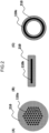
- FIG. 2 contains schematic drawings illustrating exemplary shapes of the one or more of Nb alloy strips.
- FIG. 2(A) illustrates the case where each strip shape of the one or more of Nb alloy strips is a core 110a, but the above shape is not limited to be a core (specifically, a core for a multi-core wire).
- Each strip shape of the one or more of Nb alloy strips may be a sheet 110b as illustrated in FIG. 2(B) , or may be a pipe 110c as illustrated in FIG. 2(C).
- FIG. 2 shows the aspects of the cases where each strip of the one or more of Nb alloy strips having the respective shapes (i.e., forms) is covered with the first stabilizer 210.
- each strip shape of the one or more of Nb alloy strips is a core 110a as illustrated in FIG. 2 (A)
- each strip shape of the one or more of Nb alloy strips is a sheet 110b as illustrated in FIG. 2(B)
- each strip shape of the one or more of Nb alloy strips is a pipe 110c as illustrated in FIG. 2(C)
- FIG. 3 contains schematic drawings illustrating the Nb 3 Sn superconducting wire and the NbTi wire.
- FIGS. 3(A) and (B) illustrate cross sections of the Nb 3 Sn superconducting wire and the NbTi wire, respectively.
- the Nb 3 Sn superconducting wire 130 the Nb 3 Sn superconducting cores 150 of a multi-core wire are covered with the second stabilizer 310 and/or embedded in the second stabilizer 310.
- the Nb 3 Sn superconducting wire 130 may be an ordinarily used Nb 3 Sn superconducting wire that can be obtained from a Nb 3 Sn precursor wire described below by means of an annealing treatment.
- the second stabilizer 310 is made of a normal conducting metal material, and may be preferably made of the material selected from the group consisting of copper metal, copper alloy, silver metal, and silver alloy.
- the Nb 3 Sn superconducting wire 130 may have a diffusion barrier layer 320.
- the diffusion barrier layer 320 can avoid the diffusion of element when manufactured from the Nb 3 Sn precursor wire described below by means of an annealing treatment.
- Such a diffusion barrier layer 320 may be made of tantalum (Ta), niobium (Nb), or alloy thereof. By the use of these metals, the diffusion of Sn and Nb is more preferably avoided.
- the NbTi cores 160 of a multi-core wire thereof may be covered with the third stabilizer 330 and/or embedded in the third stabilizer 330.
- the third stabilizer 330 is made of a normal conducting metal material, and may be preferably made of the material selected from the group consisting of copper metal, copper alloy, silver metal, and silver alloy.
- the first to third stabilizers may be different or the same.
- each of the one or more of NbTi cores 160 can use a NbTi core that is ordinarily used and available.
- the composition of Ti in the alloy of NbTi falls into a range from 8 at% or more to 90 at% or less.
- each of the one or more of NbTi cores can be processed by wire drawing, and can maintain higher properties. It is more preferable that the composition of Ti in the NbTi alloy falls into a range from 50 at% or more to 70 at% or less.
- each of a portion where each of the one or more of Nb alloy strips 110 and each of the one or more of Nb 3 Sn superconducting cores 150 are in contact with each other through the Nb 3 Sn superconducting core layer 170 interposed therebetween and each bare surface of the one or more of Nb alloy strips 110 and each bare surface of the one or more of NbTi cores 160 are in mutual contact may be preferably covered by means of a crimp tube 180 as illustrated in FIG. 1 .
- the crimp tube 180 is not particularly limited as long as it has a Vickers hardness of 60 Hv or more, and is exemplarily made of the material selected from the group consisting of tantalum (Ta), niobium (Nb), copper-nickel alloy (CuNi), and stainless steel. Each of these materials has a Vickers hardness from 60 Hv or more to 300 Hv or less.
- the material of the crimp tube 180 is tantalum (Ta) in order to suppress a reaction during an annealing treatment.
- each length (more specifically, the length of the crimp tube 180) of the above portion where the one or more of Nb alloy strips 110 and the one or more of Nb 3 Sn superconducting cores 150 are in contact and covered and the above portion where the one or more of Nb alloy strips 110 and the one or more of NbTi cores 160 are in mutual contact and covered is a range from 10 mm or more to 30 mm or less. In a case of falling into this range, good superconducting properties can be obtained by the sufficient contact.
- each length of the above portions being in contact and covered as described above it is more preferable to fall within a range from 10 mm or more to 20 mm or less, and it is furthermore preferable to fall within a range from 15 mm or more to 25 mm or less.
- the Nb 3 Sn superconducting wire 130 and the NbTi wire 140 are jointed without using any environmentally hazardous substance such as Pb or Cd as well as with maintaining a high critical current even in a magnetic field environment of 0.5 T to 1.0 T. Therefore, the superconducting joint structural body 100 of the present invention can be applied to a nuclear magnetic resonance (NMR) apparatus for high field use.
- NMR nuclear magnetic resonance
- the superconducting joint structural body 100 of the present invention do not use any environmentally hazardous substance, there is no need to apply for exclusion of Restriction of Hazardous Substances (RoHS) Directive and so on. This also enables to significantly reduce costs for manufacturing NMR.
- the superconducting joint structural body of the present invention preferably satisfies the critical current characteristics of at least 50 A or more, at 4.2 K, in a magnetic field environment of 0.6 T.
- FIG. 4 is a flowchart of steps for manufacturing the superconducting joint structural body of the present invention.
- step of "S410" One end of a joint strip having one or more of Nb alloy strips to which the element M is added and a Nb 3 Sn superconducting wire having one or more of Nb 3 Sn superconducting cores are jointed.
- the superconducting joint structural body 100 of the present invention is manufactured by the step of "S410" of a first jointing step and the step of "S420" of a second jointing step.
- the Nb 3 Sn superconducting wire can be manufactured from a Nb 3 Sn superconducting precursor wire ( FIG. 5 ) described below without decreasing the properties of the one or more of Nb alloy strips even after performing an annealing treatment for forming Nb 3 Sn in the first jointing step. And, the one or more of Nb alloy strips and the Nb 3 Sn superconducting wire can be jointed through the Nb 3 Sn superconducting layer formed on each of the one or more of Nb alloy strips.
- the second jointing step it is only necessary to mechanically joint the one or more of Nb alloy strips and the NbTi wire, and thus the superconducting joint between the Nb 3 Sn superconducting wire and the NbTi wire can be performed without using any environmentally hazardous substances such as Pb and Cd.
- the Nb 3 Sn superconducting precursor wire is used.
- the Nb 3 Sn superconducting precursor wire the one or more of Nb cores that are embedded in a matrix that contains at least Cu and Sn can be used.
- Such a Nb 3 Sn superconducting precursor wire is distributed on the market and commercially available.
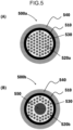
- FIG. 5 contains schematic drawings illustrating an exemplary Nb 3 Sn superconducting precursor wire used for manufacturing the superconducting joint structural body of the present invention.
- the one or more of Nb cores 510 may be embedded in a Cu-Sn matrix 520a.
- the Cu-Sn matrix 520a is made of an alloy of Cu and Sn, preferably having a Sn content in a range from 5 at% or more to 10 at% or less. In a case of falling into this range, the above Cu-Sn matrix reacts with the one or more of Nb cores 510 embedded therein, thereby forming the one or more of Nb 3 Sn superconducting cores 150 (see FIG. 1 ). As a result, workability of the core wire can be achieved.
- the Nb 3 Sn superconducting precursor wire 500a may preferably have a diffusion barrier layer 530 around the Cu-Sn matrix 520a. This enables to suppress the diffusion of Nb from the one or more of Nb cores 510 and the diffusion of Sn from the Cu-Sn matrix 520a during an annealing treatment described below.
- the diffusion barrier layer 530 may be made of tantalum (Ta), niobium (Nb), or alloy thereof.
- the Nb 3 Sn superconducting precursor wire 500a may preferably have a stabilizer 540 around the Cu-Sn matrix 520a. This enables to easily detour the current, even in the case where the one or more of Nb 3 Sn superconducting cores returned back to the normal conduction mode due to thermal disturbance after performing the diameter reduction treatment.
- the material of the stabilizer 540 is the same material as the above second stabilizer 310.
- a Nb 3 Sn superconducting precursor wire 500b illustrated in FIG. 5(B) differs from the Nb 3 Sn superconducting precursor wire 500a illustrated in FIG. 5(A) in the following respects: in the Nb 3 Sn superconducting precursor wire 500b illustrated in FIG. 5(B) , a Cu matrix 520b and a Sn matrix 550 are separately provided and the one or more of Nb cores 510 are embedded only in the Cu matrix 520b.
- a case where the matrix in which the one or more of Nb cores are embedded is separated into the Cu matrix and the Sn matrix is also regarded as a case where the one or more of Nb cores are embedded in the matrix that contains Cu and Sn.
- an embodiment of the "matrix that contains at least Cu and Sn" described in the specification of the present application includes, in addition to an embodiment containing at least Cu and Sn in the same matrix as illustrated in FIG. 5(A) (that is, an embodiment in which the matrix that contains Cu is the same as the matrix containing Sn), an embodiment in which the matrix that contains at least Cu and the matrix that contains at least Sn are separated as illustrated in FIG. 5(B) .
- the embodiment of the "one or more of Nb cores embedded in a matrix that contains at least Cu and Sn” exemplarily includes: an embodiment in which the one or more of Nb cores are embedded in the Cu-Sn matrix made of an alloy of Cu and Sn as illustrated in FIG.
- the matrix made of Cu and the matrix made of Sn are separately provided and the one or more of Nb cores are embedded only in the matrix made of Sn; and an embodiment in which the matrix made of Cu and the matrix made of Sn are separately provided and the one or more of Nb cores are embedded only in the matrix made of Cu as illustrated in FIG. 5(B) .
- the Sn matrix 550 falls into a range from 10 at% or more to 60 at% or less with regard to the total of the Cu matrix 520b and the Sn matrix 550.
- the matrix preferably reacts with the one or more of NbTi cores 510, thereby forming the one or more of Nb 3 Sn superconducting cores 150 ( FIG. 1 ). As a result, workability of the core wire can be achieved.
- the Nb 3 Sn superconducting precursory wire 500b may be provided with a stabilizer 540 around the Cu matrix 520b.
- Nb 3 Sn superconducting precursor wires illustrated in FIG. 5 is merely exemplary ones. Besides them, the Nb 3 Sn superconducting precursor wires disclosed in " WO 2018/198515 A1 " and “ WO2021/024529 A1 ", for example can be also used. From these points of view, it is only necessary that the one or more of NbTi cores 510 are embedded in a matrix that contains at least Cu and Sn, but the matrix (specifically, Cu matrix, Sn matrix, or Cu-Sn matrix) may further contain zinc (Zn), germanium (Ge), gallium (Ga), magnesium (Mg), aluminum (Al), or titanium (Ti).
- FIG. 6 is a flowchart of the first jointing step.
- FIG. 7 illustrates a series of procedures of the first jointing step.
- the first jointing step (S410) illustrated in FIG. 4 will be detailed referring to a case where the joint strip 120 illustrated in FIG. 1 is used as the joint strip, and the Nb 3 Sn superconducting precursor wire 500a illustrated in FIG. 5(A) is used as the Nb 3 Sn superconducting precursor wire.
- the step of "S411" The one or more of Nb alloy strips (specifically, the one or more of cores) 110a are exposed from one end of the joint strip 120, wherein each of the one or more of Nb alloy strips 110a is covered with the first stabilizer 210.
- the above exposure method is performed by means of chemical corrosion, mechanical polishing, or a combination thereof, but is not particularly limited to these means. It is preferable that the exposed length falls into a range from 10 mm or more to 30 mm or less. In a case of falling into this range, good superconducting properties can be obtained by the sufficient contact when being bundled with the one or more of Nb cores 510 described below. It is more preferable that the exposed length falls into the range from 10 mm or more to 20 mm or less.
- the step of"S412" The one or more of Nb cores 510 are exposed from one end of the Nb 3 Sn superconducting precursor wire 500a in which the one or more of Nb cores 510 are embedded in a matrix that contains at least Cu and Sn (i.e., Cu-Sn matrix 520a).
- the above exposure method is performed by means of chemical corrosion, mechanical polishing, or a combination thereof, but is not particularly limited to these means. It is preferable that chemical corrosion and mechanical polishing take place in this order. This makes the exposure easier even in the case where the Nb 3 Sn superconducting precursor wire 500a has the diffusion barrier layer 530. It is preferable that the exposed length falls into a range from 10 mm or more to 30 mm or less.
- the exposed length falls into a range from 10 mm or more to 20 mm or less. In this case, it is paid for attention so as not to completely remove the matrix that contains Cu and Sn. This is because the remaining Cu-Sn is essential for formation of the Nb 3 Sn layer.
- the step of "S413" The exposed one or more of Nb alloy strips 110a and the exposed one or more of Nb cores 510 are bundled together.
- the above bundling method may be performed by means of matching, twisting, entangling, winding or the like, but is not particularly limited to these means.
- the step of "5414" The one or more of Nb alloy strips 110a and the one or more of Nb cores 510 that are bundled together in the step of "S413" are crimped.
- the above crimping method is performed by the steps of: applying a pressure to the one or more of Nb alloy strips 110a and the one or more of Nb cores 510 that are bundled together, thereby exposing each bare surface of them; and making each exposed bare surface of them in close contact with each other.
- the Nb 3 Sn superconducting layer on each of the above bared surfaces is formed, and the one or more of Nb alloy strips and the one or more of Nb cores that are bundled together can be jointed thereby.
- the preferred method is as follows: the bundled portion is covered with the crimp tube 180, and then the pressure is applied to the one or more of Nb alloy strips 110a and the one or more of Nb cores 510 that are bundled together in a perpendicular direction to a longitudinal direction thereof, thereby crimping them. As a result, the bare surfaces of them can be in close contact with each other.
- the crimp tube 180 is as already explained referring to FIG. 1 . It is preferable that the pressure to be applied falls into a range from 100 MPa or more to 1 GPa or less. In a case of falling into this range, the close contact between the above bare surfaces can be promoted. It is more preferable that the pressure to be applied falls into a range from 300 MPa or more to 500 MPa or less. In a case of falling into this range, the close contact between the above bare surfaces can be promoted without causing wire breakage.
- the step of"S415" The joint strip 120 that contains the one or more of Nb alloy strips and the one or more of Nb cores that are crimped together and the Nb 3 Sn superconducting precursor wire 500a are annealed.
- the annealing treatment may be an ordinary annealing treatment employed to form the Nb 3 Sn superconducting wire from the Nb 3 Sn superconducting precursor wire 500a.
- the one or more of Nb cores 510 reacts with the Cu-Sn matrix 520a to become the one or more of Nb 3 Sn superconducting cores 150, and concurrently the Nb 3 Sn superconducting layer 170 can be formed on each bare surface of the one or more of Nb alloy strips and the one or more of Nb cores that are bundled together. Since in the present invention, the one or more of Nb alloy strips to which the element M making the recovery temperature and the recrystallization temperature of Nb increase is added are used, the superconducting properties of the Nb alloy strip do not decrease even after the conventional annealing treatment is performed.
- the annealing treatment is performed under the conditions of the following: in vacuum or in an inert gas atmosphere of argon (Ar), helium (He) or the like, within the temperature range from 600°C or more to 800°C or less.
- Ar argon
- He helium
- the annealing treatment time varies depending on the length of the Nb 3 Sn superconducting precursor wire 500a and the number of multi-core wires, and exemplarily falls into a range from 5 hours or more to 300 hours or less.
- the annealing treatment conditions may be more preferably performed in two stages within the above temperature range.
- Exemplary the annealing treatment conditions may include, in vacuum or an inert gas atmosphere, the stage of a duration of 50 hours or more to 150 hours or less and a temperature range from 300°C or more to 500°C or less; and the subsequent stage of a duration of 50 hours or more to 150 hours or less and a temperature range of 600°C or more to 800°C or less.
- Such a two-stage annealing treatment enables to promote, while maintaining the high superconducting properties of the one or more of Nb alloy strips, formation of the uniform one or more of Nb 3 Sn superconducting cores 150 as well as formation of the Nb 3 Sn superconducting layer 170 on each of the above bare surfaces.
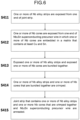
- FIG. 8 is a flowchart of the second jointing step.
- FIG. 9 illustrates a series of procedures of the second jointing step.
- the step of "S421” The one or more of Nb alloy strips 110a are exposed from the other end of the joint strip 120 wherein each of the one or more of Nb alloy strips 110a is covered with the first stabilizer 210.
- the step of "S421” may be a method similar to exposure method in the step of"S411". It is preferable that the exposed length falls into a range from 10 mm or more to 30 mm or less. In a case of falling into this range, good superconducting properties can be obtained by the sufficient contact when being bundled with the one or more of Nb cores 160 described below. It is more preferable that the exposed length falls into a range from 15 mm or more to 25 mm or less.
- the other end of the joint strip 120 is jointed with the Nb 3 Sn superconducting wire 130 in the above first jointing step.
- the step of "S422" The one or more of NbTi cores 160 are exposed from one end of the NbTi wire 140.
- the above exposure method is performed by means of chemical corrosion, mechanical polishing, or a combination thereof, but is not particularly limited to these means. It is preferable that the exposed length falls into a range from 10 mm or more to 30 mm or less. In a case of falling into this range, good superconducting properties can be obtained by the sufficient contact when being bundled with the one or more of Nb alloy strips 110a exposed in the step of "S421". It is more preferable that the exposed length falls into a range from 15 mm or more to 25 mm or less.
- the step of "S423" The exposed one or more of Nb alloy strips 110a and the exposed one or more of NbTi cores 160 are bundled together.
- the above bundling method may be performed by means of matching, twisting, entangling, winding or the like, but is not particularly limited to these means.
- the step of "S424" The one or more of Nb alloy strips and the one or more of NbTi cores that are bundled together in the step of "S423" are crimped.
- the above crimping method is performed by the steps of: applying the pressure to the one or more of Nb alloy strips 110a and the one or more of NbTi cores 160 that are bundled together, thereby exposing each bare surface of them; and making each exposed bare surface of them in close contact with each other.
- the one or more of Nb alloy strips and the one or more of NbTi cores that are bundled together can be jointed on the bare surfaces of them.
- the preferred method is as follows: the bundled portion is covered with the crimp tube 180, and the thus the pressure is applied to the one or more of Nb alloy strips 110a and the one or more of NbTi cores 160 that are bundled together in a perpendicular direction to a longitudinal direction thereof, thereby crimping them.
- the bare surfaces of them can be in close contact with each other.
- the pressure to be applied falls into a range from 100 MPa or more to 1 GPa or less. In a case of falling into this range, the close contact between the above bare surfaces can be promoted. It is more preferable that the pressure to be applied falls to a range from 300 MPa or more to 500 MPa or less. In a case of falling into this range, the close contact between the above bare surfaces can be promoted without causing wire breakage.
- NbTi wire National Bureau of Standards (NBS) standard sample
- NBS National Bureau of Standards
- the annealing treatment was performed under the following conditions: in vacuum and at 685°C for 100 hours. Compositional percentage of Ti contained in the NbTi cores was 60 at%.
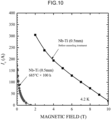
- the wire was immersed in liquid helium, and critical current was measured when applying an external magnetic field. The results are summarized in FIG. 10 .
- FIG. 10 is a drawing illustrating the critical current characteristics of the NbTi wire before and after performing an annealing treatment.
- the critical current of NbTi wire before performing the annealing treatment shows a high value, but the critical magnetic field of the NbTi wire dramatically decreases after performing the annealing treatment at the temperature of more than 600°C corresponding to the temperature of formation of Nb 3 Sn, and also the critical current thereof decreased.
- the critical current of the NbTi wire after performing the annealing treatment shows to be less than 100 A even in a magnetic field of 0.2 T. The reason is as follows.
- Nb alloy wires a Nb alloy wire having a wire diameter of 1 mm wherein the Nb alloy wire is made of nineteen Nb-2at%Hf cores embedded in a Cu matrix; and a Nb alloy wire having a wire diameter of 1 mm wherein the Nb alloy wire is made of nineteen Nb-4at%Ta-1at% Hf cores embedded in a Cu matrix, the changes in the critical current characteristics before and after annealing treatment were examined.
- the above Nb alloy wires were manufactured as follows.
- Nb-2at%Hf alloy melted by arc melting and Nb-4at%Ta-1at%Hf alloy melted by arc melting was processed into a rod having a diameter slightly less than 6 mm by swaging processing, and inserted into a Cu tube having an outer/inner diameter of 8 mm/6 mm.
- Each resultant was subjected to swaging processing and die drawing processing to separately manufacture a Cu/Nb-Hf single-core wire having an outer diameter of 1 mm and a Cu/Nb-Ta-Hf single-core wire having an outer diameter of 1 mm.
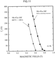
- FIG. 11 is a drawing illustrating the critical current characteristics of the Nb-Ta-Hf wire (Nb-4at%Ta-1at%Hf wire) before and after performing an annealing treatment.
- the Nb-Ta-Hf wire is denoted as Nb-4Ta-1Hf. It is noted that the drawing does not illustrate the critical current characteristics of the Nb-Hf wire before and after the annealing treatment.
- the critical current of the Nb-Ta-Hf wire only slightly decreases even after performing the annealing treatment at the temperature of more than 600°C corresponding to the temperature of formation of Nb 3 Sn, and still maintains the high critical current even at 0.5 T.
- the Nb-Hf wire maintains a high critical current at 0.8 T even after performing the annealing treatment.
- the Nb alloy wire to which the element of Hf, Ta or the like is added as the element M increases the recovery temperature and the recrystallization temperature of Nb, and thus it has been found to maintain the high critical current even after performing the annealing treatment at the temperature equal to or higher than the temperature of formation of Nb 3 Sn. It has been demonstrated from the above results that the Nb alloy to which the element M is added is effective for the joint strip to which the Nb 3 Sn superconducting precursor wire is jointed.
- Example 1 the Nb-Ta-Hf (specifically, Nb-4at%Ta-1at%Hf) wire used in the above “Reference Example” was employed as the joint strip, and the superconducting joint structural body in which the Nb 3 Sn superconducting wire and the NbTi wire were jointed according to the method illustrated in FIG. 4 was manufactured.
- Nb 3 Sn precursor wire As a Nb 3 Sn precursor wire, the Nb 3 Sn precursor wire in which 1045 Nb cores are embedded in a matrix formed by separately arranging Cu and Sn as illustrated in FIG. 5(B) was prepared.
- a diffusion barrier layer made of Nb was provided between the area that contains Cu, Sn and Nb and the outermost Cu.
- the compositional percentage of Sn in the matrix was 14 at%, each diameter of the Nb cores was 11 ⁇ m, and the thickness of the diffusion barrier layer was 15 ⁇ m.
- the NbTi wire used herein was same as the NbTi wire used in Reference Example.
- the above Nb-Ta-Hf wire as the joint strip was jointed with the above Nb 3 Sn superconducting wire (see the step of "S410" in FIG. 4 ). Specifically, the above Nb-Ta-Hf wire was cut into 8 cm lengths, and the Nb-Ta-Hf cores as the Nb alloy strips were exposed from one end thereof (see the step of "S411" in FIGS. 6 and 7 ). A 15 mm-long end portion of the above Nb-Ta-Hf wire was immersed in nitric acid to remove the Cu (copper) matrix of the stabilizer.
- the Nb cores were exposed from one end of the Nb 3 Sn superconducting precursor wire (see the step of "S412" in FIGS. 6 and 7 ).
- the outermost Cu was removed, with nitric acid, from a 15 mm-long end portion of the Nb 3 Sn superconducting precursor wire, and the diffusion barrier layer was then removed by mechanically polishing with a sandpaper. In this process, it was confirmed that the Cu matrix and the Sn matrix that are around the Nb cores remains without being completely removed.
- the exposed Nb-Ta-Hf cores and the exposed Nb cores were bundled by means of twisting and entangling (see the step of "S413" in FIGS. 6 and 7 ).
- the bundled portion was crimped (see the step of "S414" in FIGS. 6 and 7 ).
- the bundled portion was inserted into a tantalum (Ta) tube as a crimp tube having an outer diameter/inner diameter of 3.6 mm/2.5 mm, and then a pressure of 400 MPa was applied thereto by means of a hydraulic press.
- the Nb-Ta-Hf wire and the Nb 3 Sn superconducting precursor wire that include the crimped portion were annealed (see the step of "S415" in FIGS. 6 and 7 ).
- the annealing treatment was performed under the following conditions: in vacuum and at 390°C for 100 hours, and then at 685°C for 100 hours.
- the above Nb 3 Sn superconducting wire was produced from the above Nb 3 Sn superconducting precursor wire, and the above Nb-Ta-Hf wire and the above Nb 3 Sn superconducting wire were jointed through the Nb 3 Sn superconducting layer interposed therebetween.
- the other end of the above Nb-Ta-Hf wire and the above NbTi wire having the NbTi cores were jointed (see the step of "Step S420" in FIG. 4 ).
- the Nb-Ta-Hf cores were exposed from the other end of the above Nb-Ta-Hf wire (see the step of "Step S421" in FIGS. 8 and 9 ).
- a 20 mm-long end portion of the Nb-Ta-Hf wire was immersed in nitric acid, to remove the Cu matrix (i.e., the third stabilizer).
- the NbTi cores were exposed from one end of the above NbTi wire (see the step of "Step S422" in FIGS. 8 and 9 ).
- the Cu matrix was removed, with nitric acid, from a 20 mm-long end portion of the above NbTi wire.
- the exposed Nb-Ta-Hf cores and the exposed NbTi cores were bundled by means of twisting and entangling (see the step of "Step S423" in FIGS. 8 and 9 ).
- the bundled portion was crimped (see the step of "Step S424" in FIGS. 8 and 9 ).
- the bundled portion was inserted into a tantalum (Ta) tube as a crimp tube having an outer diameter/inner diameter of 3.6 mm/2.5 mm, and then a pressure of 400 MPa was applied thereto by means of a hydraulic press.
- Ta tantalum
- a pressure of 400 MPa was applied thereto by means of a hydraulic press.
- Example 1 The superconducting joint structural body of "Example 1" was observed under a scanning electron microscope (SEM, from JEOL Ltd.) equipped with an energy dispersive X-ray analyzer (EDS) and an element mapping thereof was examined. The results are illustrated in FIG. 12 .
- SEM scanning electron microscope
- EDS energy dispersive X-ray analyzer
- FIG. 12 contains results of observation of a cross section of the joint portion between the joint strip and the Nb 3 Sn superconducting wire in the superconducting joint structural body, observed under the electron microscope.
- the cores are in close contact with each other by means of crimping (see the step of "Step S414" in FIG. 6 ).
- the Nb 3 Sn superconducting cores in the Nb 3 Sn superconducting wire are a multi-core wire and in mutual contact as well as that the Nb-Ta-Hf core of the joint strip and the Nb 3 Sn superconducting core are in close contact with each other.
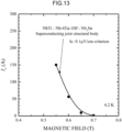
- FIG. 13 is a drawing illustrating the critical current characteristics of the superconducting joint structural body of "Example 1".
- the superconducting joint structural body i.e., NbTi-Nb-4at%Ta-1at%Hf-Nb 3 Sn superconducting joint structural body
- NbTi-Nb-4Ta-1Hf-Nb 3 Sn superconducting joint structural body is denoted as "NbTi-Nb-4Ta-1Hf-Nb 3 Sn superconducting joint structural body”.
- the superconducting joint structural body of “Example 1" shows the high critical current exceeding 150 A even in the case where 0.55 T is applied.
- Example 2 a superconducting joint structural body was manufactured in the same way as “Example 1” except that the Nb-Hf (Nb-2at%Hf) wire used in the above “Reference Example” was employed as the joint strip.
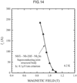
- the superconducting joint structural body of “Example 2” was observed by means of SEM and the critical current characteristics thereof were examined. The results were illustrated in FIG. 14 .
- FIG. 14 is a drawing illustrating the critical current characteristics of the superconducting joint structural body of "Example 2".
- the superconducting joint structural body i.e., NbTi-Nb-2at%Hf-Nb 3 Sn superconducting joint structural body
- NbTi-Nb-2Hf-Nb 3 Sn superconducting joint structural body is denoted as "NbTi-Nb-2Hf-Nb 3 Sn superconducting joint structural body”.
- the superconducting joint structural body of “Example 2" shows the high critical current exceeding 150 A even in the case where a magnetic field (0.9 T) higher than the magnetic field in the superconducting joint structural body in “Example 1" was applied.
- a magnetic field 0.9 T
- the superconducting joint structural body in which the Nb 3 Sn superconducting wire and the NbTi wire are jointed without using any environmentally hazardous substances such as Pb and Cd as well as with maintaining the high superconducting properties can be provided.
- Hf is preferred as the element M.
- the joint structural body in which the Nb 3 Sn superconducting wire and the NbTi wire can be jointed without using any environmentally hazardous substances such as Pb and Cd has excellent properties and can be used in magnetic field environment of 0.5 T to 1.0 T.
- the joint structural body according to the present invention can be applied to a superconducting joint of a magnet for a nuclear magnetic resonance (NMR) apparatus.
Landscapes
- Engineering & Computer Science (AREA)
- Power Engineering (AREA)
- Superconductors And Manufacturing Methods Therefor (AREA)
- Manufacturing Of Electrical Connectors (AREA)
- Connections Effected By Soldering, Adhesion, Or Permanent Deformation (AREA)
Applications Claiming Priority (2)
| Application Number | Priority Date | Filing Date | Title |
|---|---|---|---|
| JP2021095620 | 2021-06-08 | ||
| PCT/JP2022/019931 WO2022259803A1 (fr) | 2021-06-08 | 2022-05-11 | Structure de connexion supraconductrice de tige de fil supraconducteur en nb3sn et tige de fil en nbti, son procédé de production et appareil à résonance magnétique nucléaire l'utilisant |
Publications (3)
| Publication Number | Publication Date |
|---|---|
| EP4354664A1 true EP4354664A1 (fr) | 2024-04-17 |
| EP4354664A4 EP4354664A4 (fr) | 2025-06-04 |
| EP4354664B1 EP4354664B1 (fr) | 2026-01-28 |
Family
ID=84424859
Family Applications (1)
| Application Number | Title | Priority Date | Filing Date |
|---|---|---|---|
| EP22819987.3A Active EP4354664B1 (fr) | 2021-06-08 | 2022-05-11 | Corps structurel à joint superconducteur de fil supraconducteur en nb3sn et fil en nbti, son procédé de fabrication et appareil à résonance magnétique nucléaire l'utilisant |
Country Status (4)
| Country | Link |
|---|---|
| US (1) | US12500011B2 (fr) |
| EP (1) | EP4354664B1 (fr) |
| JP (1) | JP7587889B2 (fr) |
| WO (1) | WO2022259803A1 (fr) |
Families Citing this family (1)
| Publication number | Priority date | Publication date | Assignee | Title |
|---|---|---|---|---|
| CN121460293B (zh) * | 2026-01-07 | 2026-05-05 | 西安聚能超导线材科技有限公司 | 一种铜铝基体NbTi超导线材及其制备方法 |
Family Cites Families (13)
| Publication number | Priority date | Publication date | Assignee | Title |
|---|---|---|---|---|
| US3422529A (en) | 1963-12-09 | 1969-01-21 | North American Rockwell | Method of making a superconductive joint |
| FR2052122A5 (fr) * | 1969-07-18 | 1971-04-09 | Thomson Csf | |
| US4584547A (en) | 1983-12-30 | 1986-04-22 | General Electric Company | Superconducting joint for superconducting wires and coils |
| DE4017553C1 (fr) * | 1990-05-31 | 1991-09-19 | Kernforschungszentrum Karlsruhe Gmbh, 7500 Karlsruhe, De | |
| JPH065345A (ja) * | 1992-04-24 | 1994-01-14 | Furukawa Electric Co Ltd:The | 異種超電導線材の接続方法 |
| JP2910586B2 (ja) * | 1994-11-11 | 1999-06-23 | 株式会社神戸製鋼所 | Nb▲3▼Sn超電導線材 |
| JP4041389B2 (ja) * | 2002-12-12 | 2008-01-30 | 株式会社神戸製鋼所 | 超電導接続構造体およびその製法 |
| US11133120B2 (en) * | 2014-04-30 | 2021-09-28 | Christopher Mark Rey | Superconductor cable or superconductor cable-in-conduit-conductor with clocking feature |
| JP6270209B2 (ja) * | 2014-03-20 | 2018-01-31 | 国立研究開発法人物質・材料研究機構 | Nb3Sn超伝導線材の製造方法 |
| WO2016143416A1 (fr) * | 2015-03-10 | 2016-09-15 | 株式会社日立製作所 | Pièce de connexion de fil supraconducteur |
| US11476017B2 (en) | 2017-04-27 | 2022-10-18 | National Institute For Materials Science | Method for producing Nb3Sn superconducting wire, precursor for Nb3Sn superconducting wire, and Nb3Sn superconducting wire using same |
| WO2021024529A1 (fr) | 2019-08-07 | 2021-02-11 | 国立研究開発法人物質・材料研究機構 | PRÉCURSEUR POUR MATÉRIAU DE FIL SUPRACONDUCTEUR Nb3Sn, SON PROCÉDÉ DE PRODUCTION ET PROCÉDÉ DE PRODUCTION DE MATÉRIAU DE FIL SUPRACONDUCTEUR Nb3Sn L'UTILISANT |
| CN111243818B (zh) * | 2020-03-13 | 2021-07-27 | 中国科学院电工研究所 | 一种铌三锡超导线和铌钛超导线的超导接头及其制备方法 |
-
2022
- 2022-05-11 WO PCT/JP2022/019931 patent/WO2022259803A1/fr not_active Ceased
- 2022-05-11 EP EP22819987.3A patent/EP4354664B1/fr active Active
- 2022-05-11 JP JP2023527578A patent/JP7587889B2/ja active Active
- 2022-05-11 US US18/562,234 patent/US12500011B2/en active Active
Also Published As
| Publication number | Publication date |
|---|---|
| EP4354664A4 (fr) | 2025-06-04 |
| WO2022259803A1 (fr) | 2022-12-15 |
| JPWO2022259803A1 (fr) | 2022-12-15 |
| US12500011B2 (en) | 2025-12-16 |
| EP4354664B1 (fr) | 2026-01-28 |
| US20240242857A1 (en) | 2024-07-18 |
| JP7587889B2 (ja) | 2024-11-21 |
Similar Documents
| Publication | Publication Date | Title |
|---|---|---|
| CN109643593B (zh) | 金属超导线的扩散屏障 | |
| US12476025B2 (en) | Diffusion barriers for metallic superconducting wires | |
| JPH0377608B2 (fr) | ||
| EP0234071B1 (fr) | Procédé de fabrication d'un conducteur électrique supraconducteur | |
| JP6719141B2 (ja) | Nb3Sn超伝導線材の製造方法、Nb3Sn超伝導線材用の前駆体、及びこれを用いたNb3Sn超伝導線材 | |
| CN1358237A (zh) | 约束的细丝铌基超导复合体及其制造方法 | |
| EP4354664B1 (fr) | Corps structurel à joint superconducteur de fil supraconducteur en nb3sn et fil en nbti, son procédé de fabrication et appareil à résonance magnétique nucléaire l'utilisant | |
| EP1364074A2 (fr) | Composite supraconducteur a base de niobium a filaments contraint et procede de fabrication | |
| JP6704589B2 (ja) | Nb3Al超伝導線材用前駆体線材及びNb3Al超伝導線材 | |
| KR102423559B1 (ko) | 금속성 초전도성 와이어를 위한 확산 배리어 | |
| WO2004040663A2 (fr) | Composite supraconducteur a base de niobium a filament contraint et procede de fabrication | |
| JP4723306B2 (ja) | Nb3Al系超電導線材の製造方法、Nb3Al系超電導線材製造用一次複合材及びその製造方法、並びにNb3Al系超電導線材製造用多芯複合材 | |
| JP6232450B2 (ja) | 酸化物超電導線材 | |
| KR20070120497A (ko) | 초전도 선재의 제조 방법 | |
| JP3428771B2 (ja) | Nb3Sn系化合物超電導線材 | |
| JP2517867B2 (ja) | V3 Si超電導極細多芯線材の製造法 | |
| JPH0443513A (ja) | Nb↓3Sn超電導線材の製造方法 | |
| HK1089549B (en) | Superconductive wire material, superconductive multi-conductor wire using the same and method for producing the same | |
| HK1089549A1 (zh) | 超导线,使用该超导线的超导复丝线及其制造方法 | |
| JPH0711925B2 (ja) | Nb―Ti系超電導線 | |
| JPH07122127A (ja) | 酸化物超電導線材 |
Legal Events
| Date | Code | Title | Description |
|---|---|---|---|
| STAA | Information on the status of an ep patent application or granted ep patent |
Free format text: STATUS: THE INTERNATIONAL PUBLICATION HAS BEEN MADE |
|
| PUAI | Public reference made under article 153(3) epc to a published international application that has entered the european phase |
Free format text: ORIGINAL CODE: 0009012 |
|
| STAA | Information on the status of an ep patent application or granted ep patent |
Free format text: STATUS: REQUEST FOR EXAMINATION WAS MADE |
|
| 17P | Request for examination filed |
Effective date: 20231031 |
|
| AK | Designated contracting states |
Kind code of ref document: A1 Designated state(s): AL AT BE BG CH CY CZ DE DK EE ES FI FR GB GR HR HU IE IS IT LI LT LU LV MC MK MT NL NO PL PT RO RS SE SI SK SM TR |
|
| DAV | Request for validation of the european patent (deleted) | ||
| DAX | Request for extension of the european patent (deleted) | ||
| A4 | Supplementary search report drawn up and despatched |
Effective date: 20250506 |
|
| RIC1 | Information provided on ipc code assigned before grant |
Ipc: H10N 60/01 20230101ALN20250428BHEP Ipc: H02G 15/34 20060101ALN20250428BHEP Ipc: H10N 60/80 20230101ALI20250428BHEP Ipc: H02G 1/14 20060101ALI20250428BHEP Ipc: H01R 43/048 20060101ALI20250428BHEP Ipc: H01R 4/20 20060101ALI20250428BHEP Ipc: H01F 6/06 20060101ALI20250428BHEP Ipc: H01B 12/10 20060101ALI20250428BHEP Ipc: H01R 4/68 20060101AFI20250428BHEP |
|
| GRAP | Despatch of communication of intention to grant a patent |
Free format text: ORIGINAL CODE: EPIDOSNIGR1 |
|
| RIC1 | Information provided on ipc code assigned before grant |
Ipc: H01R 4/68 20060101AFI20250922BHEP Ipc: H01B 12/10 20060101ALI20250922BHEP Ipc: H01F 6/06 20060101ALI20250922BHEP Ipc: H01R 4/20 20060101ALI20250922BHEP Ipc: H01R 43/048 20060101ALI20250922BHEP Ipc: H02G 1/14 20060101ALI20250922BHEP Ipc: H10N 60/80 20230101ALI20250922BHEP Ipc: H02G 15/34 20060101ALN20250922BHEP Ipc: H10N 60/01 20230101ALN20250922BHEP |
|
| STAA | Information on the status of an ep patent application or granted ep patent |
Free format text: STATUS: GRANT OF PATENT IS INTENDED |
|
| INTG | Intention to grant announced |
Effective date: 20251030 |
|
| GRAS | Grant fee paid |
Free format text: ORIGINAL CODE: EPIDOSNIGR3 |
|
| GRAA | (expected) grant |
Free format text: ORIGINAL CODE: 0009210 |
|
| STAA | Information on the status of an ep patent application or granted ep patent |
Free format text: STATUS: THE PATENT HAS BEEN GRANTED |
|
| AK | Designated contracting states |
Kind code of ref document: B1 Designated state(s): AL AT BE BG CH CY CZ DE DK EE ES FI FR GB GR HR HU IE IS IT LI LT LU LV MC MK MT NL NO PL PT RO RS SE SI SK SM TR |
|
| REG | Reference to a national code |
Ref country code: CH Ref legal event code: F10 Free format text: ST27 STATUS EVENT CODE: U-0-0-F10-F00 (AS PROVIDED BY THE NATIONAL OFFICE) Effective date: 20260128 Ref country code: GB Ref legal event code: FG4D |
|
| REG | Reference to a national code |
Ref country code: DE Ref legal event code: R096 Ref document number: 602022029428 Country of ref document: DE |
|
| REG | Reference to a national code |
Ref country code: IE Ref legal event code: FG4D |
|
| REG | Reference to a national code |
Ref country code: NL Ref legal event code: MP Effective date: 20260128 |
|
| PG25 | Lapsed in a contracting state [announced via postgrant information from national office to epo] |
Ref country code: NL Free format text: LAPSE BECAUSE OF FAILURE TO SUBMIT A TRANSLATION OF THE DESCRIPTION OR TO PAY THE FEE WITHIN THE PRESCRIBED TIME-LIMIT Effective date: 20260128 |
|
| REG | Reference to a national code |
Ref country code: AT Ref legal event code: MK05 Ref document number: 1882802 Country of ref document: AT Kind code of ref document: T Effective date: 20260128 |
|
| PG25 | Lapsed in a contracting state [announced via postgrant information from national office to epo] |
Ref country code: RS Free format text: LAPSE BECAUSE OF FAILURE TO SUBMIT A TRANSLATION OF THE DESCRIPTION OR TO PAY THE FEE WITHIN THE PRESCRIBED TIME-LIMIT Effective date: 20260428 |
|
| PG25 | Lapsed in a contracting state [announced via postgrant information from national office to epo] |
Ref country code: ES Free format text: LAPSE BECAUSE OF FAILURE TO SUBMIT A TRANSLATION OF THE DESCRIPTION OR TO PAY THE FEE WITHIN THE PRESCRIBED TIME-LIMIT Effective date: 20260128 |
|
| PG25 | Lapsed in a contracting state [announced via postgrant information from national office to epo] |
Ref country code: PL Free format text: LAPSE BECAUSE OF FAILURE TO SUBMIT A TRANSLATION OF THE DESCRIPTION OR TO PAY THE FEE WITHIN THE PRESCRIBED TIME-LIMIT Effective date: 20260128 |
|
| PG25 | Lapsed in a contracting state [announced via postgrant information from national office to epo] |
Ref country code: GR Free format text: LAPSE BECAUSE OF FAILURE TO SUBMIT A TRANSLATION OF THE DESCRIPTION OR TO PAY THE FEE WITHIN THE PRESCRIBED TIME-LIMIT Effective date: 20260429 |
|
| REG | Reference to a national code |
Ref country code: LT Ref legal event code: MG9D |
|
| PG25 | Lapsed in a contracting state [announced via postgrant information from national office to epo] |
Ref country code: LT Free format text: LAPSE BECAUSE OF FAILURE TO SUBMIT A TRANSLATION OF THE DESCRIPTION OR TO PAY THE FEE WITHIN THE PRESCRIBED TIME-LIMIT Effective date: 20260128 |
|
| PGFP | Annual fee paid to national office [announced via postgrant information from national office to epo] |
Ref country code: DE Payment date: 20260317 Year of fee payment: 5 |
|
| PG25 | Lapsed in a contracting state [announced via postgrant information from national office to epo] |
Ref country code: NO Free format text: LAPSE BECAUSE OF FAILURE TO SUBMIT A TRANSLATION OF THE DESCRIPTION OR TO PAY THE FEE WITHIN THE PRESCRIBED TIME-LIMIT Effective date: 20260428 |
|
| PG25 | Lapsed in a contracting state [announced via postgrant information from national office to epo] |
Ref country code: SE Free format text: LAPSE BECAUSE OF FAILURE TO SUBMIT A TRANSLATION OF THE DESCRIPTION OR TO PAY THE FEE WITHIN THE PRESCRIBED TIME-LIMIT Effective date: 20260128 Ref country code: AT Free format text: LAPSE BECAUSE OF FAILURE TO SUBMIT A TRANSLATION OF THE DESCRIPTION OR TO PAY THE FEE WITHIN THE PRESCRIBED TIME-LIMIT Effective date: 20260128 Ref country code: FI Free format text: LAPSE BECAUSE OF FAILURE TO SUBMIT A TRANSLATION OF THE DESCRIPTION OR TO PAY THE FEE WITHIN THE PRESCRIBED TIME-LIMIT Effective date: 20260128 |
|
| PG25 | Lapsed in a contracting state [announced via postgrant information from national office to epo] |
Ref country code: HR Free format text: LAPSE BECAUSE OF FAILURE TO SUBMIT A TRANSLATION OF THE DESCRIPTION OR TO PAY THE FEE WITHIN THE PRESCRIBED TIME-LIMIT Effective date: 20260128 |
|
| PG25 | Lapsed in a contracting state [announced via postgrant information from national office to epo] |
Ref country code: PT Free format text: LAPSE BECAUSE OF FAILURE TO SUBMIT A TRANSLATION OF THE DESCRIPTION OR TO PAY THE FEE WITHIN THE PRESCRIBED TIME-LIMIT Effective date: 20260528 Ref country code: IS Free format text: LAPSE BECAUSE OF FAILURE TO SUBMIT A TRANSLATION OF THE DESCRIPTION OR TO PAY THE FEE WITHIN THE PRESCRIBED TIME-LIMIT Effective date: 20260528 |
|
| PG25 | Lapsed in a contracting state [announced via postgrant information from national office to epo] |
Ref country code: LV Free format text: LAPSE BECAUSE OF FAILURE TO SUBMIT A TRANSLATION OF THE DESCRIPTION OR TO PAY THE FEE WITHIN THE PRESCRIBED TIME-LIMIT Effective date: 20260128 |
|
| PG25 | Lapsed in a contracting state [announced via postgrant information from national office to epo] |
Ref country code: BG Free format text: LAPSE BECAUSE OF FAILURE TO SUBMIT A TRANSLATION OF THE DESCRIPTION OR TO PAY THE FEE WITHIN THE PRESCRIBED TIME-LIMIT Effective date: 20260128 |